


DATA SHEET
Solid State Relay
PS7212-1A
4-PIN SOP 100 V BREAK DOWN VOLTAGE
1-ch Optical Coupled MOS FET
DESCRIPTION
The PS7212-1A is a solid state relay containing GaAs LEDs on the light emitting side (input side) and normally
open (N.O.) contact MOS FETs on the output side.
It is suitable for analog signal control because of its low offset and high linearity.
FEATURES
• Small and thin package (4-pin SOP, Height = 2.1 mm)
• 1 channel type (1 a output)
• Low LED operating current (IF = 2 mA)
• Designed for AC/DC switching line changer
• Low offset voltage
• Ordering number of taping product: PS7212-1A-E3, E4, F3, F4
OCMOS FET
APPLICATIONS
• Laptop PC, PDA
• Modem card
• Telephone, FAX
• Measurement equipment
The information in this document is subject to change without notice. Before using this document, please
confirm that this is the latest version.
Not all devices/types available in every country. Please check with local NEC representative for
availability and additional information.
Document No. P13927EJ4V0DS00 (4th edition)
Date Published October 1999 NS CP(K)
Printed in Japan
The mark
••••
shows major revised points.
©
1998, 1999

PS7212-1A
–0.05
+0.08
2.05
–0.05
+0.08
0.05
0.40
4.0±0.5
2.54
+0.10
–0.05
0.25 M
PACKAGE DIMENSIONS
in millimeters
–0.05
+0.10
0.15
TOP VIEW
43
1. LED Anode
2. LED Cathode
3. MOS FET
4. MOS FET
12
7.0±0.3
4.4
0.5±0.3
2
Data Sheet P13927EJ4V0DS00

ORDERING INFORMATION
PS7212-1A
Part Number Package Packing Style
Application Part Number
PS7212-1A 4-pin SOP Magazine case 100 pcs PS7212-1A
PS7212-1A -E3 Embossed Tape 900 pcs/reel
PS7212-1A -E4
PS7212-1A -F3 Embossed Tape 3 500 pcs/reel
PS7212-1A -F4
For the application of the Safety Standard, following part number should be used.
*1
ABSOLUTE MAXIMUM RATINGS (TA = 25 °°°°C, unless otherwise specified)
Parameter Symbol Ratings Unit
Diode Forward Current (DC) I
Reverse Voltage V
Power Dissipation P
Peak Forward Current
*1
MOS FET Break Down Voltage V
Continuous Load Current I
Pulse Load Current
*2
(AC/DC Connection)
Power Dissipation P
Isolation Voltage
*3
Total Power Dissipat i on P
Operating Ambient Temperature T
Storage Temperature T
F
R
D
FP
I
L
L
LP
I
D
50 mA
5.0 V
50 mW
1A
100 V
200 mA
400 mA
300 mW
BV 1 500 Vr.m.s.
T
A
stg
350 mW
−
40 to +80
−
40 to +100
°
C
°
C
*1
PW = 100 µs, Duty Cycle = 1 %
*1
PW = 100 ms, 1 shot
*2
AC voltage for 1 minute at TA = 25 °C, RH = 60 % between input and output
*3
Data Sheet P13927EJ4V0DS00
3
RECOMMENDED OPERATING CONDITIONS (TA = 25 °°°°C)
Parameter Symbol MIN. TYP. MAX. Unit
PS7212-1A
LED Operating Current I
LED Off Voltage V
F
F
21020mA
00.5V
ELECTRICAL CHARACTERISTICS (TA = 25 °°°°C)
Parameter Symbol Conditions MIN. TYP. MAX. Unit
Diode Forward Voltage V
Reverse Current I
MOS FET Off-state Leakage Current I
Output Capacitance C
Coupled LED On-state Current I
On-state Resistance R
Turn-on Time
Turn-off Time
*1
*1
Isolation Resistance R
Isolation Capacitance C
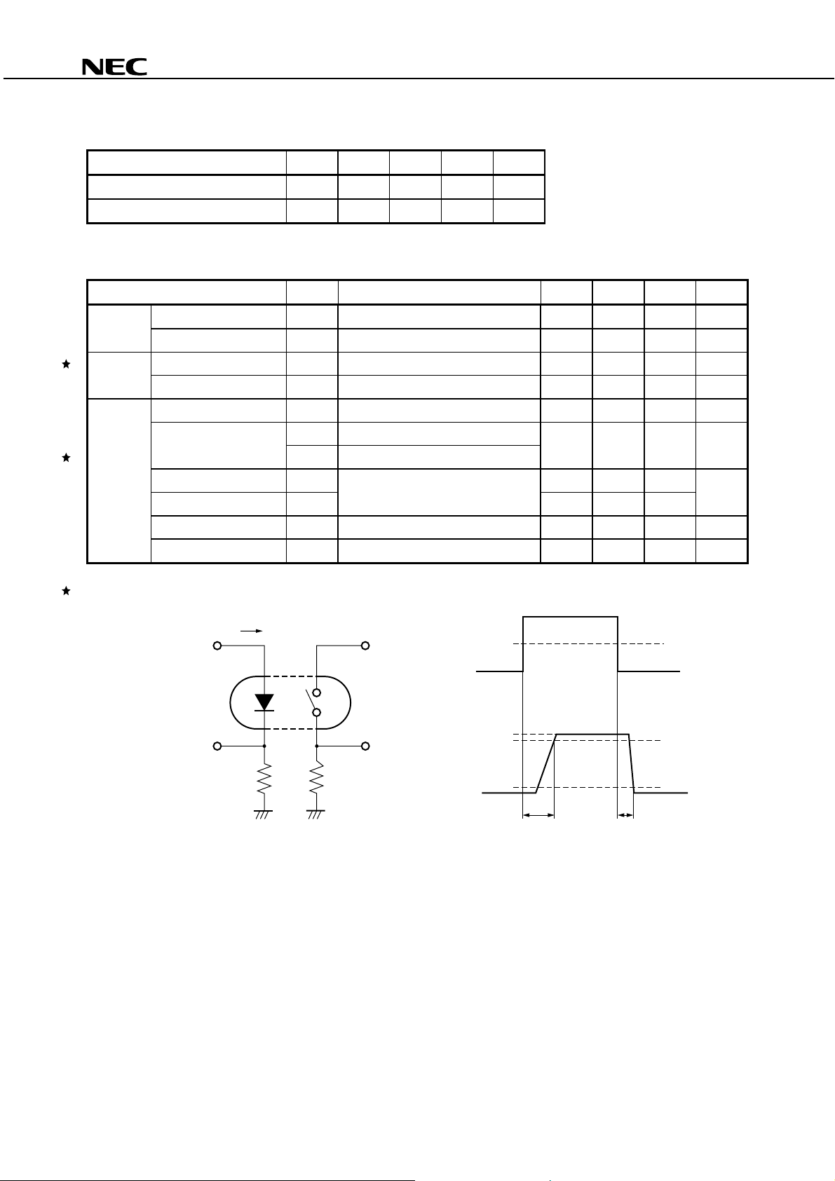
Test Circuit for Switching Time
*1
F
R
Loff
out
FonIL
on1IF
on2IF
R
on
t
off
t
I-O
I-O
IF = 10 mA 1.2 1.4 V
VR = 5 V 5.0
VD = 100 V 0.03 1.0
VD = 0 V, f = 1 MHz 57 pF
= 200 mA 2.0 mA
= 10 mA, IL = 10 mA 3.0 6.0
= 10 mA, IL = 200 mA, t ≤ 10 ms
IF = 10 mA, VO = 5 V, PW ≥ 10 ms 0.35 1.0 ms
I-O
V
= 1.0 kV
V = 0 V, f = 1 MHz 0.5 pF
µ
A
µ
A
Ω
0.08 0.2
DC
10
9
Ω
I
F
Pulse Input
Input monitor monitorV
R
in
R
L
V
L
Input
50 %
0
O
VO = 5 V
90 %
Output
10 %
t
on
t
off
4
Data Sheet P13927EJ4V0DS00

TYPICAL CHARACTERISTICS (TA = 25 °°°°C, unless otherwise specified)
PS7212-1A
MAXIMUM FORWARD CURRENT vs.
AMBIENT TEMPERATURE
100
(mA)
80
F
60
40
20
Maximum Forward Current I
0
–25 0 25 50
Ambient Temperature T
FORWARD VOLTAGE vs.
AMBIENT TEMPERATURE
1.6
1.4
(V)
F
1.2
1.0
Forward Voltage V
75
A
(˚C)
IF = 50 mA
80
30 mA
20 mA
10 mA
5 mA
1 mA
100
MAXIMUM LOAD CURRENT vs.
AMBIENT TEMPERATURE
300
250
(mA)
L
200
150
100
50
Maximum Load Current I
0
–25 0 25 50
Ambient Temperature TA (˚C)
OUTPUT CAPACITANCE vs.
APPLIED VOLTAGE
125
100
(pF)
out
75
50
25
Output Capacitance C
80
75
f = 1 MHz
100
0.8
–25 0 25 50
Ambient Temperature T
A
OFF-STATE LEAKAGE CURRENT vs.
APPLIED VOLTAGE
–3
10
–4
(A)
10
Loff
–5
10
–6
10
–7
10
–8
10
Off-state Leakage Current I
–9
10
4020060
Applied Voltage VD (V)
TA = 80 ˚C
25 ˚C
80
75
100
(˚C)
120
100
Data Sheet P13927EJ4V0DS00
40
60
80 120
D
(V)
20
0
Applied Voltage V
LOAD CURRENT vs. LOAD VOLTAGE
200
(mA)
L
–1.0–1.5 –0.5 0.5 1.0 1.50
Load Current I
100
–100
–200
Load Voltage VL (V)
100
IF = 10 mA
5

NORMALIZED ON-STATE RESISTANCE vs.
AMBIENT TEMPERATURE
3.0
on
2.5
2.0
Normalized to 1.0
A
= 25 ˚C,
at T
I
F
= 10 mA,
L
= 10 mA
I
PS7212-1A
ON-STATE RESISTANCE DISTRIBUTION
30
25
20
n = 50 pcs,
I
F
= 10 mA,
I
L
= 10 mA
1.5
1.0
0.5
Normalized On-state Resistance R
0.0
–25 0 25 50
Ambient Temperature T
A
(˚C)
75
TURN-ON TIME vs. FORWARD CURRENT
2.5
VO = 5 V VO = 5 V
2.0
(ms)
on
1.5
1.0
Turn-on Time t
0.5
0
5
Forward Current IF (mA)
15 20
2510
100
30
15
Number (pcs)
10
5
0
2.5 3.5
3.0 4.0
4.5
On-state Resistance Ron (Ω)
TURN-OFF TIME vs. FORWARD CURRENT
0.5
0.4
(ms)
off
0.3
0.2
Turn-off Time t
0.1
0
5
15 20 30
10
Forward Current IF (mA)
25
30
25
20
15
Number (pcs)
10
5
0
6
TURN-ON TIME DISTRIBUTION
n = 50 pcs,
I
F
= 10 mA,
O
= 5 V
V
0.30
Turn-on Time ton (ms)
0.40
0.45
0.500.35
30
25
20
15
Number (pcs)
10
Data Sheet P13927EJ4V0DS00
TURN-OFF TIME DISTRIBUTION
5
0
0.08 0.100.06
Turn-off Time t
0.12 0.14
off
(ms)
n = 50 pcs,
I
F
= 10 mA,
O
= 5 V
V

PS7212-1A
NORMALIZED TURN-ON TIME vs.
AMBIENT TEMPERATURE
3.0
on
2.5
2.0
1.5
1.0
0.5
Normalized Turn-on Time t
0.0
–25
Remark
0
Ambient Temperature T
The graphs indicate nominal characteristics.
25
Normalized to 1.0
at TA = 25 ˚C,
IF = 10 mA,
VO = 5 V
50
A
(˚C)
75
100
NORMALIZED TURN-OFF TIME vs.
AMBIENT TEMPERATURE
3.0
Normalized to 1.0
off
2.5
2.0
1.5
1.0
0.5
Normalized Turn-off Time t
0.0
–25
0
Ambient Temperature TA (˚C)
25
at TA = 25 ˚C,
IF = 10 mA,
VO = 5 V
50
75
100
Data Sheet P13927EJ4V0DS00
7
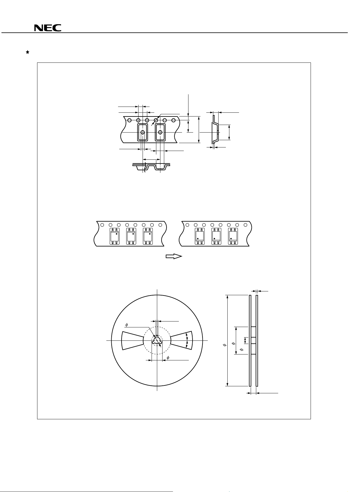
TAPING SPECIFICATIONS (in millimeters)
Outline and Dimensions (Tape)
2.0±0.1
4.0±0.1
1.55±0.1
1.75±0.1
PS7212-1A
2.4±0.1
1.55±0.1
8.0±0.1
Tape Direction
PS7212-1A-E3 PS7212-1A-E4
Outline and Dimensions (Reel)
4.6±0.1
5.5±0.1
12.0±0.2
7.4±0.1
0.3
2.0
2.0±0.5
13.0±0.5
15˚
15˚
21.0±0.8
180
60
13.0±0.5
13.0±1.0
Packing: 900 pcs/reel
8
Data Sheet P13927EJ4V0DS00

Outline and Dimensions (Tape)
2.0±0.1
4.0±0.1
1.55±0.1
1.75±0.1
PS7212-1A
2.4±0.1
1.55±0.1
8.0±0.1
Tape Direction
PS7212-1A-F3
Outline and Dimensions (Reel)
4.6±0.1
1
2
0
5.5±0.1
˚
12.0±0.2
0.3
PS7212-1A-F4
7.4±0.1
1.5
2.0±0.5
1.5±0.5
6
0
˚
Packing: 3 500 pcs/reel
Data Sheet P13927EJ4V0DS00
21.0±0.8
φ
6.0±1
330
φ
80±5.0
13.0±0.5
φ
φ
12.4
+2.0
–0.0
9

RECOMMENDED SOLDERING CONDITIONS
(1) Infrared reflow soldering
• Peak reflow temperature 235 °C (package surface temperature)
• Time of temperature higher than 210 °C 30 seconds or less
• Number of reflows Two
• Flux Rosin flux containing small amount of chlorine (The flux with a
maximum chlorine content of 0.2 Wt % is recommended.)
Recommended Temperature Profile of Infrared Reflow
(heating)
to 10 s
235 ˚C (peak temperature)
210 ˚C
to 30 s
100 to 160 ˚C
PS7212-1A
60 to 120 s
(preheating)
Package Surface Temperature T (˚C)
Time (s)
(2) Dip soldering
• Temperature 260 °C or below (molten solder temperature)
• Time 10 seconds or less
• Number of times One
• Flux Rosin flux containing small amount of chlorine (The flux with a maximum chlorine content of
0.2 Wt % is recommended.)
(3) Cautions
•Fluxes
Avoid removing the residual flux with freon-based and chlorine-based cleaning solvent.
10
Data Sheet P13927EJ4V0DS00

[MEMO]
PS7212-1A
Data Sheet P13927EJ4V0DS00
11

PS7212-1A
CAUTION
Within this device there exists GaAs (Gallium Arsenide) material which is a
harmful substance if ingested. Please do not under any circumstances break the
hermetic seal.
• The information in this document is subject to change without notice. Before using this document, please
confirm that this is the latest version.
• No part of this document may be copied or reproduced in any form or by any means without the prior written
consent of NEC Corporation. NEC Corporation assumes no responsibility for any errors which may appear in
this document.
• NEC Corporation does not assume any liability for infringement of patents, copyrights or other intellectual property
rights of third parties by or arising from use of a device described herein or any other liability arising from use
of such device. No license, either express, implied or otherwise, is granted under any patents, copyrights or other
intellectual property rights of NEC Corporation or others.
• Descriptions of circuits, software, and other related information in this document are provided for illustrative
purposes in semiconductor product operation and application examples. The incorporation of these circuits,
software, and information in the design of the customer's equipment shall be done under the full responsibility
of the customer. NEC Corporation assumes no responsibility for any losses incurred by the customer or third
parties arising from the use of these circuits, software, and information.
• While NEC Corporation has been making continuous effort to enhance the reliability of its semiconductor devices,
the possibility of defects cannot be eliminated entirely. To minimize risks of damage or injury to persons or
property arising from a defect in an NEC semiconductor device, customers must incorporate sufficient safety
measures in its design, such as redundancy, fire-containment, and anti-failure features.
• NEC devices are classified into the following three quality grades:
"Standard", "Special", and "Specific". The Specific quality grade applies only to devices developed based on a
customer designated "quality assurance program" for a specific application. The recommended applications of
a device depend on its quality grade, as indicated below. Customers must check the quality grade of each device
before using it in a particular application.
Standard: Computers, office equipment, communications equipment, test and measurement equipment,
audio and visual equipment, home electronic appliances, machine tools, personal electronic
equipment and industrial robots
Special: Transportation equipment (automobiles, trains, ships, etc.), traffic control systems, anti-disaster
systems, anti-crime systems, safety equipment and medical equipment (not specifically designed
for life support)
Specific: Aircraft, aerospace equipment, submersible repeaters, nuclear reactor control systems, life
support systems or medical equipment for life support, etc.
The quality grade of NEC devices is "Standard" unless otherwise specified in NEC's Data Sheets or Data Books.
If customers intend to use NEC devices for applications other than those specified for Standard quality grade,
they should contact an NEC sales representative in advance.
M7 98. 8
 Loading...