

DATA SHEET
PHOTOCOUPLER
PS2562-1,-2, PS2562L-1,-2
HIGH ISOLATION VOLTAGE
DARLINGTON TRANSISTOR TYPE
MULTI PHOTOCOUPLER SERIES
DESCRIPTION
The PS2562-1, -2 and PS2562L-1, -2 are optically coupled isolators containing a GaAs light emitting diode and an
NPN silicon darlington connected phototransistor.
PS2562-1, -2 are in a plastic DIP (Dual In-line Package) and PS2562L-1, -2 are lead bending type (Gull-wing) for
surface mount.
FEATURES
• High isolation voltage BV = 5 000 Vr.m.s.: standard products
BV = 3 750 Vr.m.s.: VDE0884 approved products (Option)
• High current transfer ratio (CTR = 2 000 % TYP.)
• High-speed switching (tr, tf = 100 µs TYP.)
• UL approved (File No. E72422 (S) )
• CSA approved (No. CA 101391)
• BSI approved (BS415, BS7002) No. 7112
• SEMKO approved (SS4410165) No. 9317144
• NEMKO approved (NEK-HD 195S6) No. A21409
• DEMKO approved (Section 101, 137) No. 300535
• FIMKO approved (E69-89) No. 167265-08
• VDE0884 approved (Option)
APPLICATIONS
• Power supply
• Telephone/FAX.
• FA/OA equipment
• Programmable logic controller
The information in this document is subject to change without notice.
Document No. P12990EJ4V0DS00 (4th edition)
(Previous No. LC-2226)
Date Published August 1997 NS
Printed in Japan
The mark
shows major revised points.
©
1992

PACKAGE DIMENSIONS (in millimeters)
DIP Type
PS2562-1,-2,PS2562L-1,-2
6.5
3.8
4.55
MAX.
2.8
MIN.
1.25±0.15
PS2562-1 (New Package)
3
4
4.6 ± 0.35
12
1. Anode
2. Cathode
3. Emitter
4. Collector
7.62
MAX.
0.65
0.50 ± 0.10
0.25
2.54
M
0 to 15˚
6.5
3.8
4.55
MAX.
2.8
MIN.
1.25±0.15
5.1 MAX.
MAX.
0.65
2.54
PS2562-1
0.50 ± 0.10
0.25
3
4
12
1. Anode
2. Cathode
3. Emitter
4. Collector
7.62
M
0 to 15˚
PS2562L1-1
5.1 MAX.
6.5
3.8
MAX.
4.25
MAX.
2.8
MIN.
0.35
1.25±0.15
2.54
Caution New package 1ch only
0.50 ± 0.10
0.25
3
4
2
1
1. Anode
2. Cathode
3. Emitter
4. Collector
10.16
7.62
M
0 to 15˚
6.5
3.8
4.55
MAX.
2.8
MIN.
1.25±0.15
MAX.
0.65
10.2 MAX.
2.54
PS2562-2
0.50 ± 0.10
M
0.25
8
71265
34
1, 3. Anode
2, 4. Cathode
5, 7. Emitter
6, 8. Collector
7.62
0 to 15˚
2
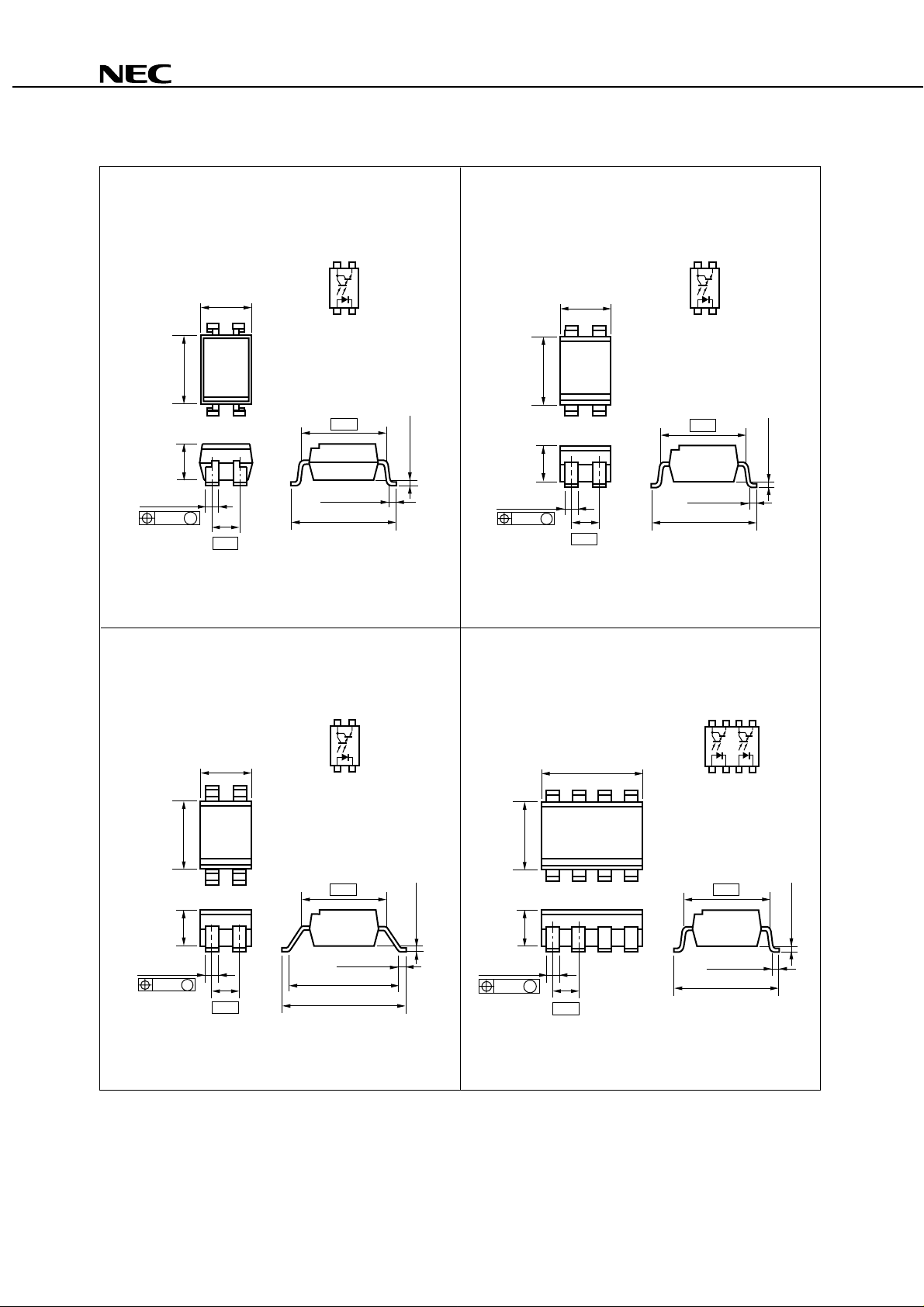
Lead Bending Type
PS2562-1,-2,PS2562L-1,-2
PS2562L-1 (New Package)
4.6 ± 0.35
6.5
3.8
MAX.
1.25±0.15
M
0.25
2.54
3
4
12
1. Anode
2. Cathode
3. Emitter
4. Collector
7.62
0.90 ± 0.25
9.60 ± 0.4
0.05 to 0.2
3.8
MAX.
1.25±0.15
0.25
6.5
M
5.1 MAX.
2.54
PS2562L-1
3
4
12
1. Anode
2. Cathode
3. Emitter
4. Collector
7.62
0.90 ± 0.25
9.60 ± 0.4
0.05 to 0.2
PS2562L2-1
5.1 MAX.
6.5
3.8
MAX.
1.25±0.15
M
0.25
2.54
Caution New package 1ch only
3
4
2
1
1. Anode
2. Cathode
3. Emitter
4. Collector
7.62
0.9 ± 0.25
10.16
12.0 MAX.
0.05 to 0.2
6.5
3.8
MAX.
1.25±0.15
0.25
M
10.2 MAX.
2.54
PS2562L-2
8
71265
34
1, 3. Anode
2, 4. Cathode
5, 7. Emitter
6, 8. Collector
7.62
0.90 ± 0.25
9.60 ± 0.4
0.05 to 0.2
3
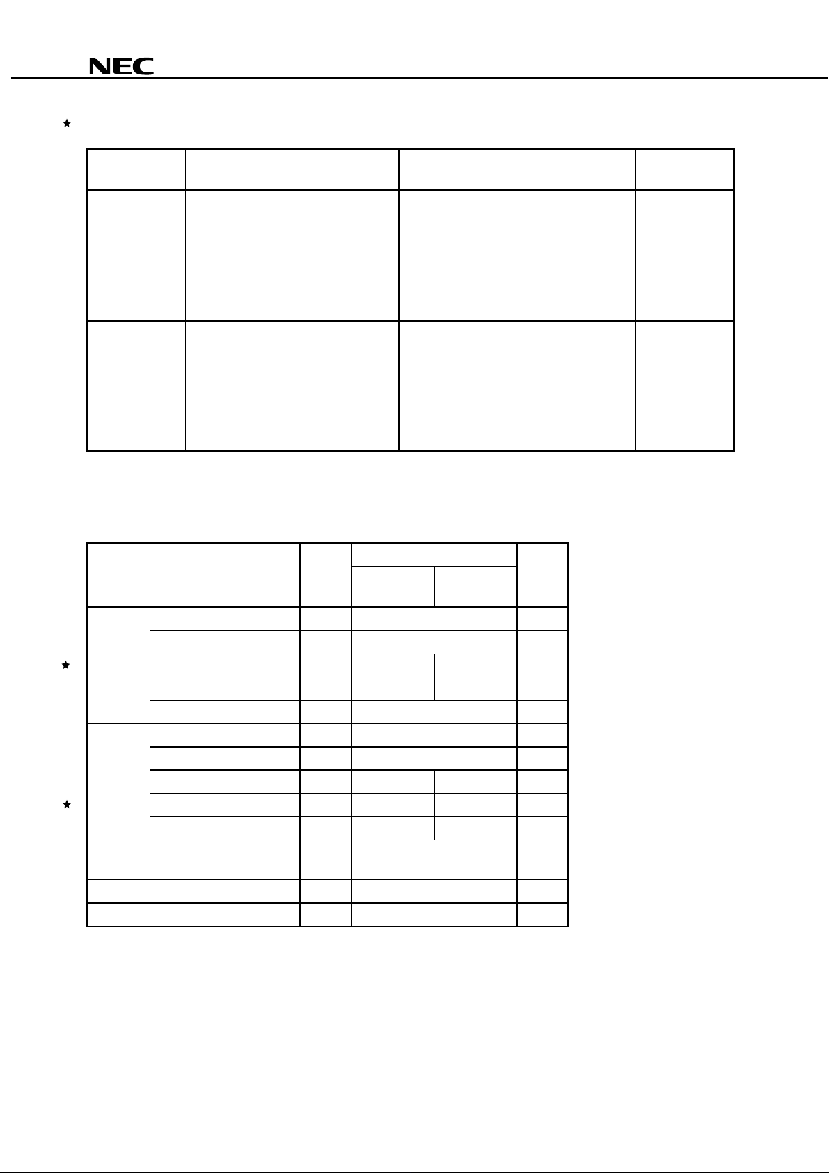
ORDERING INFORMATION
PS2562-1,-2,PS2562L-1,-2
Part Number Package Safety Standard Approval Application part
number
PS2562-1
PS2562L-1
PS2562L1-1
PS2562L2-1
PS2562-2
PS2562L-2
PS2562-1-V
PS2562L-1-V
PS2562L1-1-V
PS2562L2-1-V
4-pin DIP
4-pin DIP (lead bending surface mount)
4-pin DIP (for long distance)
4-pin DIP (for long distance surface
mount)
8-pin DIP
8-pin DIP (lead bending surface mount)
4-pin DIP
4-pin DIP (lead bending surface mount)
4-pin DIP (for long distance)
4-pin DIP (for long distance surface
Standard products PS2562-1
• UL approved • CSA approved
• BSI approved • NEMKO approved
• DEMKO approved • SEMKO approved
• FIMKO approved
PS2562-2
VDE0884 approved products (Option) PS2562-1
mount)
PS2562-2-V
PS2562L-2-V
As applying to Safety Standard, following part number should be used.
*1
8-pin DIP
8-pin DIP (lead bending surface mount)
PS2562-2
ABSOLUTE MAXIMUM RATINGS (TA = 25 °C, unless otherwise specified)
Parameter Symbol Ratings Unit
PS2562-1,
PS2562L-1
PS2562-2,
PS2562L-2
*1
Diode Reverse Voltage V
Forward Current (DC) I
R
F
6V
80 mA
Power Dissipation Derating∆PD/°C 1.5 1.2 mW/°C
I
FP
CEO
ECO
C
D
150 120 mW/ch
1A
40 V
6V
200 160 mA/ch
Power Dissipation P
Peak Forward Current
*1
Transistor Collector to Emitter Voltage V
Emitter to Collector Voltage V
Collector Current I
Power Dissipation Derating∆PC/°C 2.0 1.6 mW/°C
Power Dissipation P
Isolation Voltage
*2
Operating Ambient Temperature T
Storage Temperature T
PW = 100
*1
AC voltage for 1 minute at TA = 25 °C, RH = 60 % between input and output
*2
VDE0884 approved products (Option)
*3
µ
s, Duty Cycle = 1 %
C
200 160 mW/ch
BV 5 000
3 750
A
stg
–55 to +100
–55 to +150
*3
Vr.m.s.
°
C
°
C
4
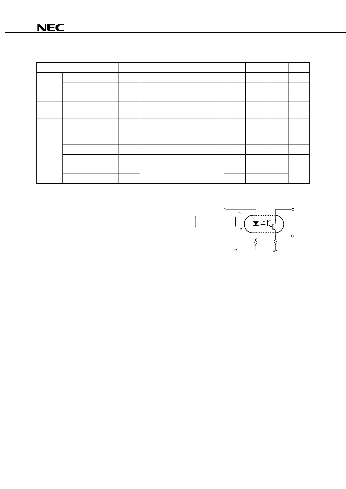
ELECTRICAL CHARACTERISTICS (TA = 25 °C)
Parameter Symbol Conditions MIN. TYP. MAX. Unit
PS2562-1,-2,PS2562L-1,-2
Diode Forward Voltage V
Reverse Current I
Terminal Capacitance C
Transistor Collector to Em itter Dar k
I
Current
Coupled
Current Transfer Ratio
Collector Satura t ion
*1
CTR IF = 1 mA, VCE = 2 V 200 2 000 %
CE (sat)IF
V
Voltage
Isolation Resistance R
Isolation Capacitance C
Rise Time
Fall Time
CTR rank (only PS2562-1, PS2562L-1)
*1
*2
*2
K : 2 000 to (%)
L : 700 to 3 400 (%)
M : 200 to 1 000 (%)
F
IF = 10 mA 1.17 1.4 V
R
VR = 5 V 5
t
V = 0 V, f = 1.0 MHz 50 pF
CEO
VCE = 40 V, IF = 0 mA 400 nA
= 1 mA, IC = 2 mA 1.0 V
I-O
I-O
V
= 1.0 kV 10
I-O
V = 0 V, f = 1.0 MHz 0.5 pF
r
t
VCC = 10 V, IC = 10 mA, RL = 100
f
t
Test circuit for switching time
*2
Ω
11
100
100
Pulse Input
PW = 1 ms
Duty Cycle = 1/10
I
F
50 Ω
µ
µ
V
V
RL = 100 Ω
A
Ω
s
CC
OUT
5

PS2562-1,-2,PS2562L-1,-2
TYPICAL CHARACTERISTICS (TA = 25 °C, unless otherwise specified)
DIODE POWER DISSIPATION vs.
AMBIENT TEMPERATURE
150
(mW)
D
100
PS2562-2
PS2562L-2
50
Diode Power Dissipation P
0255075100 125 150
Ambient Temperature T
PS2562-1
PS2562L-1
1.2 mW/˚C
1.5 mW/˚C
A
(˚C)
FORWARD CURRENT vs.
FORWARD VOLTAGE
100
50
(mA)
10
F
0.5
Forward Current I
0.1
T
A
= +100 ˚C
+60 ˚C
+25 ˚C
5
1
–25 ˚C
–55 ˚C
0 ˚C
TRANSISTOR POWER DISSIPATION
vs. AMBIENT TEMPERATURE
200
(mW)
C
150
PS2562-2
PS2562L-2
100
50
Transistor Power Dissipation P
0255075100 125 150
Ambient Temperature TA (˚C)
PS2562-1
PS2562L-1
1.6 mW/˚C
2 mW/˚C
COLLECTOR CURRENT vs.
COLLECTOR TO EMITTER VOLTAGE
160
5 mA
140
120
(mA)
C
100
80
2 mA
60
40
Collector Current I
20
1 mA
IF = 0.5 mA
0.7 0.8 0.9 1.0 1.1 1.2
Forward Voltage VF (V)
COLLECTOR TO EMITTER DARK
CURRENT vs. AMBIENT TEMPERATURE
(nA)
10 000
CEO
1000
100
10
1
Collector to Emitter Dark Current I
–50 –25 0 25 50
VCE = 2 V
5 V
10 V
24 V
40 V
Ambient Temperature T
6
1.3
A
(˚C)
75
1.4
1.5
100
0
2
Collector to Emitter Voltage VCE (V)
46810
COLLECTOR CURRENT vs.
COLLECTOR SATURATION VOLTAGE
200
100
50
(mA)
C
10
5
1
Collector Current I
0.5
0.2
0.4
0.6 0.8
Collector Saturation Voltage V
1.0
IF = 0.1 mA
1.2 1.4 1.6
CE(sat)
10 mA
5 mA
1 mA
0.5 mA
0.2 mA
(V)

PS2562-1,-2,PS2562L-1,-2
NORMALIZED CURRENT TRANSFER
RATIO vs. AMBIENT TEMPERATURE
1.4
1.2
1.0
0.8
0.6
0.4
0.2
Normalized Current Transfer Ratio CTR
–50 0–25 50
Ambient Temperature T
Normalized to 1.0
A
= 25 ˚C,
at T
F
= 1 mA, VCE = 2 V
I
25
A
SWITCHING TIME vs.
LOAD RESISTANCE
1 000
V
CC
= 5 V,
I
C
= 2 mA,
500
CTR = 2 280 %
µ
100
50
t
f
t
r
t
d
(˚C)
75
100
CURRENT TRANSFER RATIO vs.
FORWARD CURRENT
8 000
7 000
6 000
5 000
4 000
3 000
2 000
1 000
Current Transfer Ratio CTR (%)
0
0.1 0.5 1 5 10 30
Forward Current I
CURRENT TRANSFER RATIO vs.
FORWARD CURRENT
3 000
CE
= 2 V
V
2 500
2 000
1 500
F
(mA)
VCE = 2 V
10
Switching Time t ( s)
5
2
30
50 500 1 k 5 k
100
SWITCHING TIME vs.
LOAD RESISTANCE
10 000
5 000
µ
1 000
500
100
50
Switching Time t ( s)
10
1 k300
500 100 k
t
s
Load Resistance R
5 k
L
(Ω)
t
f
t
s
t
r
t
d
10 k 50 k
Load Resistance RL (Ω)
CC
= 5 V,
V
F
= 1 mA,
I
CTR = 2 280 %
1 000
500
Current Transfer Ratio CTR (%)
0
50 10010 500
Forward Current IF ( A)
FREQUENCY RESPONSE
0
V
–5
–10
–15
Normalized Gain G
–20
0.2 0.5 1 2
5
Frequency f (kHz)
µ
RL = 100 Ω
10
20
F
= 1 mA,
I
VCE = 2 V
50 100
200
7

LONG TIME CTR DEGRADATION
1.2
1.0
0.8
0.6
0.4
CTR (Relative Value)
0.2
PS2562-1,-2,PS2562L-1,-2
IF = 1 mA (TYP.)
TA = 25 oC
TA = 60 oC
0
10 10
2
10
3
10
4
10
5
10
6
Time (Hr)
8

TAPING SPECIFICATIONS (in millimeters)
Outline and Dimensions (Tape)
2.0±0.1
4.0±0.1
1.55±0.1
8.0±0.1
Taping Direction
1.55±0.1
5.6±0.1
1.75±0.1
7.5±0.1
16.0±0.3
PS2562-1,-2,PS2562L-1,-2
4.3±0.2
10.3±0.1
0.3
PS2562L-1-E3
PS2562L-1-F3
Outline and Dimensions (Reel)
R 1.0
2.0±0.5
φ
13.0±0.5
21.0±0.8
φ
PS2562L-1-E4
PS2562L-1-F4
φ
PS2562L-1-E3, E4: 250
φ
80.0±5.0
φ
PS2562L-1-F3, F4: 330
Packing: PS2562L-1-E3, E4 1 000 pcs/reel
PS2562L-1-F3, F4 2 000 pcs/reel
16.4
+2.0
–0.0
9

Outline and Dimensions (Tape)
2.0±0.1
4.0±0.1
1.55±0.1
12.0±0.1
Taping Direction
1.55±0.1
10.4±0.1
PS2562-1,-2,PS2562L-1,-2
1.75±0.1
7.5±0.1
16.0±0.3
4.3±0.2
10.3±0.1
0.3
PS2562L-2-E3 PS2562L-2-E4
Outline and Dimensions (Reel)
R 1.0
2.0±0.5
13.0±0.5
φ
21.0±0.8
φ
330
φ
80.0±5.0
φ
10
Packing: 1 000 pcs/reel
16.4
+2.0
–0.0

PS2562-1,-2,PS2562L-1,-2
RECOMMENDED SOLDERING CONDITIONS
(1) Infrared reflow soldering
• Peak reflow temperature 235 °C (package surface temperature)
• Time of temperature higher than 210 °C 30 seconds or less
• Number of reflows Three
• Flux Rosin flux containing small amount of chlorine (The flux with a
maximum chlorine content of 0.2 Wt % is recommended.)
Recommended Temperature Profile of Infrared Reflow
(heating)
to 10 s
235 ˚C (peak temperature)
210 ˚C
to 30 s
120 to 160 ˚C
60 to 90 s
(preheating)
Package Surface Temperature T (˚C)
Time (s)
Caution
Please avoid to removed the residual flux by water after the first reflow processes.
Peak temperature 235 ˚C or below
(2) Dip soldering
• Temperature 260 °C or below (molten solder temperature)
• Time 10 seconds or less
• Number of times One
• Flux Rosin flux containing small amount of chlorine (The flux with a maximum chlorine content of
0.2 Wt % is recommended.)
11

PS2562-1,-2,PS2562L-1,-2
SPECIFICATION OF VDE MARKS LICENSE DOCUMENT (VDE0884)
Parameter Symbol Speck Unit
Application classification (DIN VDE 0109)
for rated line voltages ≤ 300 Vr.m.s.
for rated line voltages ≤ 600 Vr.m.s.
Climatic test class (DIN IEC 68 Teil 1/09.80) 55/100/21
Dielectric strength maximum operating isolation voltage
Test voltage (partial discharge test procedure a for type test and random test)
pr
= 1.2 × U
U
IORM
, Pd < 5 pC
Test voltage (partial discharge test procedure b for random test)
pr
= 1.6 × U
U
IORM
, Pd < 5 pC
Highest permissible overvoltage U
IORM
U
pr
U
pr
U
TR
Degree of pollution (DIN VDE 0109) 2
Clearance distance > 7.0 mm
Creepage distance > 7.0 mm
Comparative tracking index (DIN IEC 112/VDE 0303 part 1) CTI 175
Material group (DIN VDE 0109) III a
Storage temperature range T
Operating temperature range T
stg
A
Isolation resistance, minimum value
IO
= 500 V dc at TA = 25 °C
V
IO
= 500 V dc at TA MAX. at least 100 °C
V
Ris MIN.
Ris MIN.
Safety maximum ratings (maximum permissible in case of fault, see thermal
derating curve)
Package temperature
F
Current (input current I
, Psi = 0)
Power (output or total power dissipation)
Tsi
Isi
Psi
Isolation resistance
IO
= 500 V dc at TA = 175 °C (Tsi)
V
Ris MIN.
IV
III
890
1 068
1 424 V
6 000 V
–55 to +150 °C
–55 to +100 °C
12
10
11
10
175
400
700
9
10
peak
V
peak
V
peak
peak
Ω
Ω
°C
mA
mW
Ω
12

[MEMO]
PS2562-1,-2,PS2562L-1,-2
13

[MEMO]
PS2562-1,-2,PS2562L-1,-2
14

[MEMO]
PS2562-1,-2,PS2562L-1,-2
15

PS2562-1,-2,PS2562L-1,-2
CAUTION
Within this device there exists GaAs (Gallium Arsenide) material which is a
harmful substance if ingested. Please do not under any circumstances break the
hermetic seal.
No part of this document may be copied or reproduced in any form or by any means without the prior written
consent of NEC Corporation. NEC Corporation assumes no responsibility for any errors which may appear in this
document.
NEC Corporation does not assume any liability for infringement of patents, copyrights or other intellectual
property rights of third parties by or arising from use of a device described herein or any other liability arising
from use of such device. No license, either express, implied or otherwise, is granted under any patents,
copyrights or other intellectual property rights of NEC Corporation or others.
While NEC Corporation has been making continuous effort to enhance the reliability of its semiconductor devices,
the possibility of defects cannot be eliminated entirely. To minimize risks of damage or injury to persons or
property arising from a defect in an NEC semiconductor device, customers must incorporate sufficient safety
measures in its design, such as redundancy, fire-containment, and anti-failure features.
NEC devices are classified into the following three quality grades:
"Standard", "Special", and "Specific". The Specific quality grade applies only to devices developed based on
a customer designated "quality assurance program" for a specific application. The recommended applications
of a device depend on its quality grade, as indicated below. Customers must check the quality grade of each
device before using it in a particular application.
Standard: Computers, office equipment, communications equipment, test and measurement equipment,
audio and visual equipment, home electronic appliances, machine tools, personal electronic
equipment and industrial robots
Special: Transportation equipment (automobiles, trains, ships, etc.), traffic control systems, anti-disaster
systems, anti-crime systems, safety equipment and medical equipment (not specifically designed
for life support)
Specific: Aircrafts, aerospace equipment, submersible repeaters, nuclear reactor control systems, life
support systems or medical equipment for life support, etc.
The quality grade of NEC devices is "Standard" unless otherwise specified in NEC's Data Sheets or Data Books.
If customers intend to use NEC devices for applications other than those specified for Standard quality grade,
they should contact an NEC sales representative in advance.
Anti-radioactive design is not implemented in this product.
M4 96. 5
 Loading...