


<R>
DATA SHEET
PHOTOCOUPLER
PS2561A-1,PS2561AL-1,PS2561AL1-1,PS2561AL2-1
HIGH ISOLATION VOLTAGE
SINGLE TRANSISTOR TYPE
MULTI PHOTOCOUPLER SERIES
DESCRIPTION
The PS2561A-1 is an optically coupled isolator containing a GaAs light emitting diode and an NPN silicon
phototransistor to realize an excellent cost performance.
The PS2561A-1 is in a plastic DIP (Dual In-line Package) and the PS2561AL-1 is lead bending type (Gull-wing) for
surface mount.
The PS2561AL1-1 is lead bending L1 type and the PS2561AL2-1 is lead bending L2 type (Gull-wing).
FEATURES
• High isolation voltage (BV = 5 000 Vr.m.s.)
• Ordering number of taping product: PS2561AL-1-E3, E4, F3, F4
: PS2561AL2-1-E3, E4
• Pb-Free product
• Safety standards
• UL approved: No. E72422
• CSA approved: No. CA 101391
• BSI approved: No. 7112, 7420
• SEMKO approved: No. 607784
• NEMKO approved: No. P03100141
• DEMKO approved: No. 312032
• FIMKO approved: No. FI 22778
• DIN EN60747-5-2 (VDE0884 Part2) approved: No. 40008862 (Option)
APPLICATIONS
• Power supply
• Telephone/FAX.
• FA/OA equipment
• Programmable logic controller
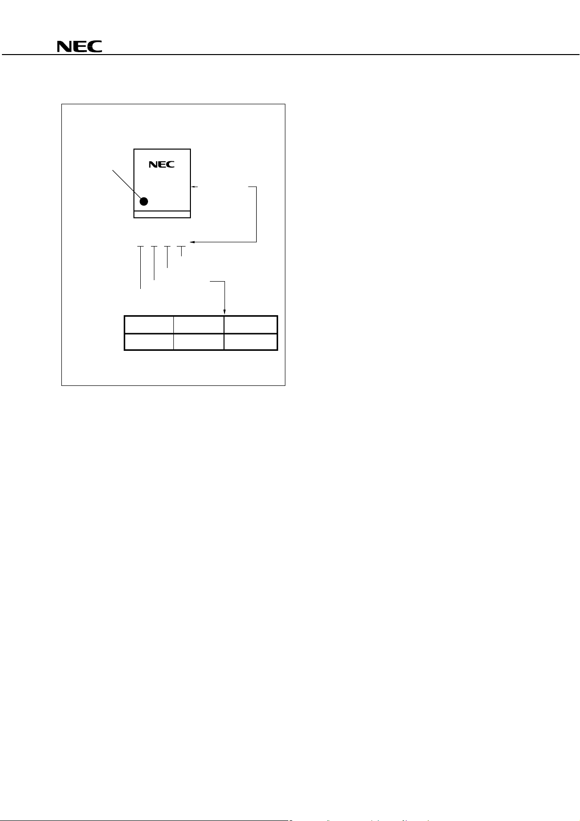
PIN CONNECTION
43
12
−NEPOC Series−
(Top View)
1. Anode
2. Cathode
3. Emitter
4. Collector
The information in this document is subject to change without notice. Before using this document, please
confirm that this is the latest version.
Not all products and/or types are available in every country. Please check with an NEC Electronics
sales representative for availability and additional information.
Document No. PN10222EJ05V0DS (5th edition)
Date Published September 2008 NS
Printed in Japan
The revised points can be easily searched by copying an "<R>" in the PDF file and specifying it in the "Find what:" field.
The mark <R> shows major revised points.
2003, 2008

PS2561A-1,PS2561AL-1,PS2561AL1-1,PS2561AL2-1
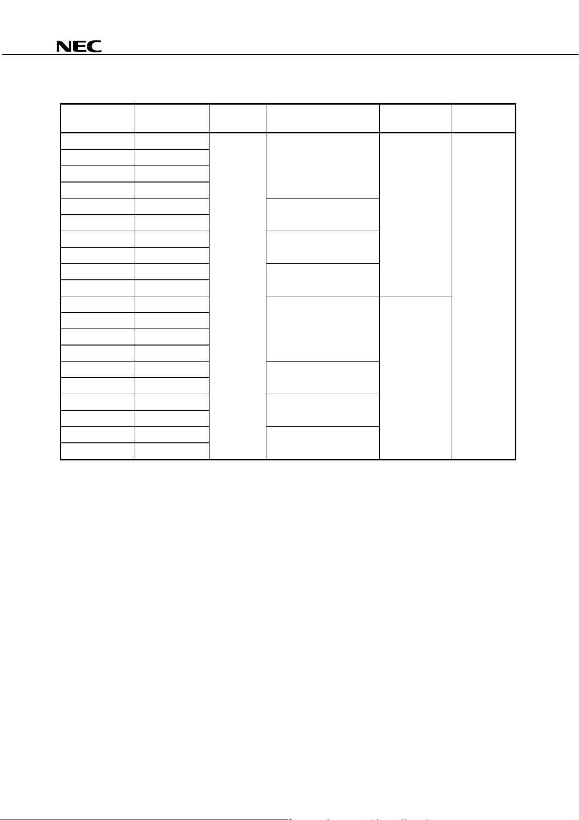
PACKAGE DIMENSIONS (UNIT : mm)
DIP Type Long Creepage Distance
1.25±0.15
Lead Bending Type (Gull-Wing) Long Creepage Distance (Gull-Wing)
1.25±0.15
0.25
6.5±0.5
4.15±0.43.2±0.4
3.5±0.3
6.5±0.5
3.5±0.3
M
PS2561A-1
4.6±0.35
3
4
2
1
0.50±0.10
2.54
PS2561AL-1
4.6±0.35
3
4
2
1
2.54
+0.1
–0.05
0.25
0.15
0 to 15˚
0.25
7.62
0.25
M
0.9±0.25
9.60±0.4
+0.1
–0.05
+0.1
–0.05
0.1
PS2561AL1-1
4.6±0.35
3
4
6.5±0.5
2
3.85
±0.4
3.15
±0.35
1.25±0.15
3.5
1
±0.3
0.50±0.1
0.25 M
2.54
0.25
10.16
+0.1
–0.05
PS2561AL2-1
4.6±0.35
3
4
6.5±0.5
2
1
0.25±0.2
3.5±0.3
1.25±0.15
0.25 M
2.54
0.25
0.9±0.25
10.16
11.8
+0.2
–0.5
0 to 15˚
+0.1
–0.05
0.25
2
Data Sheet PN10222EJ05V0DS
PS2561A-1,PS2561AL-1,PS2561AL1-1,PS2561AL2-1
<R>
MARKING EXAMPLE
No. 1 pin
Mark
2561A
NJ831
N
J
CTR Rank Code
Package
New PKG
Assembly Lot
8
31
Week Assembled
Year Assembled
(Last 1 Digit)
In-house Code
Made in Japan
JK
Made in Taiwan
Data Sheet PN10222EJ05V0DS
3
PS2561A-1,PS2561AL-1,PS2561AL1-1,PS2561AL2-1
ORDERING INFORMATION
Part Number Order Number Solder Plating
Specification
PS2561A-1 PS2561A-1-A Pb-Free Magazine case 100 pcs Standard products PS2561A-1
PS2561AL-1 PS2561AL-1-A (UL, CSA, BSI,
PS2561AL1-1 PS2561AL1-1-A NEMKO, DEMKO,
PS2561AL2-1 PS2561AL2-1-A SEMKO, FIMKO
PS2561AL-1-E3 PS2561AL-1-E3-A Embossed Tape 1 000 pcs/reel approved)
PS2561AL-1-E4 PS2561AL-1-E4-A
PS2561AL2-1-E3 PS2561AL2-1-E3-A Embossed Tape 1 000 pcs/reel
PS2561AL2-1-E4 PS2561AL2-1-E4-A
PS2561AL-1-F3 PS2561AL-1-F3-A Embossed Tape 2 000 pcs/reel
PS2561AL-1-F4 PS2561AL-1-F4-A
PS2561A-1-V PS2561A-1-V-A Magazine case 100 pcs DIN EN60747-5-2
PS2561AL-1-V PS2561AL-1-V-A (VDE0884 Part2)
PS2561AL1-1-V PS2561AL1-1-V-A Approved (option)
PS2561AL2-1-V PS2561AL2-1-V-A
PS2561AL-1-V-E3
PS2561AL-1-V-E4
PS2561AL2-1-V-E3
PS2561AL2-1-V-E4
PS2561AL-1-V-F3
PS2561AL-1-V-F4
PS2561AL-1-V-E3-A
PS2561AL-1-V-E4-A
PS2561AL2-1-V-E3-A
PS2561AL2-1-V-E4-A
PS2561AL-1-V-F3-A
PS2561AL-1-V-F4-A
Embossed Tape 1 000 pcs/reel
Embossed Tape 1 000 pcs/reel
Embossed Tape 2 000 pcs/reel
*1 For the application of the Safety Standard, following part number should be used.
Packing Style Safety Standard
Approval
Application Part
Number
*1
4
Data Sheet PN10222EJ05V0DS
PS2561A-1,PS2561AL-1,PS2561AL1-1,PS2561AL2-1
ABSOLUTE MAXIMUM RATINGS (TA = 25°C, unless otherwise specified)
Parameter Symbol Ratings Unit
Diode Reverse Voltage VR 6 V
Forward Current (DC) IF 30 mA
Power Dissipation Derating ΔPD/°C 1.5 mW/°C
Power Dissipation PD 150 mW
Peak Forward Current*1 IFP 0.5 A
Transistor Collector to Emitter Voltage VCEO 70 V
Emitter to Collector Voltage VECO 5 V
Collector Current IC 30 mA
Power Dissipation Delay
Power Dissipation PC 150 mW
Isolation Voltage*2 BV 5 000 Vr.m.s.
Operating Ambient Temperature TA −55 to +100 °C
Storage Temperature Tstg −55 to +150 °C
*1 PW = 100
μ
s, Duty Cycle = 1%
*2 AC voltage for 1 minute at TA = 25°C, RH = 60% between input and output
Pins 1-2 shorted together, 3-4 shorted together.
Δ
PC/°C 1.5 mW/°C
Data Sheet PN10222EJ05V0DS
5
 Loading...