

NEC NL8060BC31-27D, NL8060BC31-27 Specification

TFT COLOR LCD MODULE
NL8060BC31-27
NL8060BC31-27D
31cm (12.1 Type)
SVGA
DATA SHEET
DOD-PP-0214 (8th edition)
This DATA SHEET is updated document from
DOD-MD-0040(7).
All information is subject to change without notice.
Please confirm the sales representative before
starting to design your system.
Document Number: DOD-PP-0214 (8th edition)
Published date: April 2007 CP(N)
1
© NEC LCD Technologies, Ltd.
2004-2007 All rights reserved.
NL8060BC31-27/27D
INTRODUCTION
The Copyright to this document belongs to NEC LCD Technologies, Ltd. (hereinafter called "NEC").
No part of this document will be used, reproduced or copied without prior written consent of NEC.
NEC does and will not assume any liability for infringement of patents, copyrights or other intellectual
property rights of any third party arising out of or in connection with application of the products
described herein except for that directly attributable to mechanisms and workmanship thereof. No license,
express or implied, is granted under any patent, copyright or other intellectual property right of NEC.
Some electronic parts/components would fail or malfunction at a certain rate. In spite of every effort to
enhance reliability of products by NEC, the possibility of failures and malfunction might not be avoided
entirely. To prevent the risks of damage to death, human bodily injury or other property arising out
thereof or in connection therewith, each customer is required to take sufficient measures in its safety
designs and plans including, but not limited to, redundant system, fire-containment and anti-failure.
The products are classified into three quality grades: "Standard", "Special", and "Specific" of the
highest grade of a quality assurance program at the choice of a customer. Each quality grade is designed
for applications described below. Any customer who intends to use a product for application other than
that of Standard quality grade is required to contact an NEC sales representative in advance.
The Standard quality grade applies to the products developed, designed and manufactured in
accordance with the NEC standard quality assurance program, which are designed for such application as
any failure or malfunction of the products (sets) or parts/components incorporated therein a customer uses
are, directly or indirectly, free of any damage to death, human bodily injury or other property, like general
electronic devices.
Examples: Computers, office automation equipment, communications equipment, test and measurement
equipment, audio and visual equipment, home electronic appliances, machine tools, personal
electronic equipment, industrial robots, etc.
The Special quality grade applies to the products developed, designed and manufactured in accordance
with an NEC quality assurance program stricter than the standard one, which are designed for such
application as any failure or malfunction of the products (sets) or parts/components incorporated therein a
customer uses might directly cause any damage to death, human bodily injury or other property, or such
application under more severe condition than that defined in the Standard quality grade without such
direct damage.
Examples: Control systems for transportation equipment (automobiles, trains, ships, etc.), traffic control
systems, anti-disaster systems, anti-crime systems, medical equipment not specifically
designed for life support, safety equipment, etc.
The Specific quality grade applies to the products developed, designed and manufactured in accordance
with the standards or quality assurance program designated by a customer who requires an extremely
higher level of reliability and quality for such products.
Examples: Military systems, aircraft control equipment, aerospace equipment, nuclear reactor control
systems, medical equipment/devices/systems for life support, etc.
The quality grade of this product is the "Standard" unless otherwise specified in this document.
DATA SHEET DOD-PP-0214 (8th edition)
2

NL8060BC31-27/27D
CONTENTS
INTRODUCTION.......................................................................................................................................2
1. OUTLINE................................................................................................................................................4
1.1 STRUCTURE AND PRINCIPLE.......................................................................................................4
1.2 APPLICA TION...................................................................................................................................4
1.3 FEATURES.........................................................................................................................................4
2. GENERAL SPECIFICATIONS ............................................................................................................ 5
3. BLOCK DIAGRAM...............................................................................................................................6
4. DETAILED SPECIFICATIONS ...........................................................................................................7
4.1 MECHANICAL SPECIFICATIONS..................................................................................................7
4.2 ABSOLUTE MAXIMUM RATINGS.................................................................................................7
4.3 ELECTRICAL CHARACTERISTICS...............................................................................................8
4.3.1 LCD panel signal processing board .............................................................................................8
4.3.2 Backlight lamp............................................................................................................................. 9
4.3.3 Power supply voltage ripple....................................................................................................... 10
4.3.4 Fuse............................................................................................................................................ 10
4.4 POWER SUPPLY VOLTAGE SEQUENCE.....................................................................................11
4.4.1 LCD panel signal processing board ........................................................................................... 11
4.4.2 Inverter....................................................................................................................................... 11
4.5 CONNECTIONS AND FUNCTIONS FOR INTERFACE PINS..................................................... 12
4.5.1 LCD panel signal processing board ...........................................................................................12
4.5.2 Backlight lamp........................................................................................................................... 13
4.5.3 Positions of plug and socket.......................................................................................................13
4.6 DISPLAY COLORS AND INPUT DATA SIGNALS.......................................................................14
4.7 DISPLAY POSITIONS.....................................................................................................................15
4.8 SCANNING DIRECTIONS ............................................................................................................. 15
4.9 INPUT SIGNAL TIMINGS..............................................................................................................16
4.9.1 Outline of input signal timings...................................................................................................16
4.9.2 Timing characteristics................................................................................................................17
4.9.3 Input signal timing chart............................................................................................................19
4.10 OPTICS...........................................................................................................................................22
4.10.1 Optical characteristics.............................................................................................................. 22
4.10.2 Definition of contrast ratio....................................................................................................... 23
4.10.3 Definition of luminance uniformity.........................................................................................23
4.10.4 Definition of response times ....................................................................................................23
4.10.5 Definition of viewing angles....................................................................................................23
5. RELIABILITY TESTS.........................................................................................................................24
6. PRECAUTIONS ...................................................................................................................................25
6.1 MEANING OF CAUTION SIGNS ..................................................................................................25
6.2 CAUTIONS ...................................................................................................................................... 25
6.3 A TTE NTIONS .................................................................................................................................. 25
6.3.1 Handling of the product .............................................................................................................25
6.3.2 Environment............................................................................................................................... 26
6.3.3 Characteristics............................................................................................................................26
6.3.4 Other .......................................................................................................................................... 27
7. OUTLINE DRAWINGS.......................................................................................................................28
7.1 FRONT VIEW..................................................................................................................................28
7.2 REAR VIEW.....................................................................................................................................29
DATA SHEET DOD-PP-0214 (8th edition)
3

1. OUTLINE
1.1 STRUCTURE AND PRINCIPLE
Color LCD module NL8060BC31-27 and NL8060BC31-27D are composed of the amorphous silicon
thin film transistor liquid crystal display (a-Si TFT LCD) panel structure with driver LSIs for driving
the TFT (Thin Film Transistor) array and a backlight.
The a-Si TFT LCD panel structure is injected liquid crystal material into a narrow gap between the
TFT array glass substrate and a color-filter glass substrate.
Color (Red, Green, Blue) data signals from a host system (e.g. signal generator, etc.) are modulated
into best form for active matrix system by a signal processing circuit, and sent to the driver LSIs
which drive the individual TFT arrays.
The TFT array as an electro-optical switch regulates the amount of transmitted light from the
backlight assembly, when it is controlled by data signals. Color images are created by regulating the
amount of transmitted light through the TFT array of red, green and blue dots.
1.2 APPLICA TION
• For industrial use
1.3 FEATURES
• High luminance
• High contrast
• Wide viewing angle
• Wide temperature range
• 6-bit digital RGB signals
• Reversible-scan direction
• Edge light type (without inverter)
• Replaceable lamp for backlight
• Acquisition product for UL60950-1/CSA C22.2 No.60950-1-03 (File number: E170632)
• Difference between NL8060BC31-27 and NL8060BC31-27D
Polarizer surface
• Compliance with the European RoHS directive (2002/95/EC)
(From product which was produced after April. 1, 2006)
NL8060BC31-27/27D
NL8060BC31-27 NL8060BC31-27D
Clear Antiglare
DATA SHEET DOD-PP-0214 (8th edition)
4

2. GENERAL SPECIFICATIONS
Display area
Diagonal size of display
Drive system
Display color
Pixel
Pixel arrangement
Dot pitch
Pixel pitch
Module size
Weight
Contrast ratio
NL8060BC31-27/27D
246.0 (H) × 184.5 (V) mm (typ.)
31cm (12.1 inches)
a-Si TFT active matrix
262,144 colors
800 (H) × 600 (V) pixels
RGB (Red dot, Green dot, Blue dot) vertical stripe
0.1025 (H) × 0.3075 (V) mm
0.3075 (H) × 0.3075 (V) mm
280.0 (W) × 210.0 (H) × 13.0 (D) mm (typ.)
740g (typ.)
600:1 (typ.)
Viewing angle
Designed viewing direction
Polarizer surface
Polarizer pencil-hardness
Color gamut
Response time
Luminance
Signal system
Power supply voltage
Backlight
At the contrast ratio
• Horizontal: Right side 70° (typ.), Left side 70° (typ.)
• Vertical: Up side 45° (typ.), Down side 55° (typ.)
At DPS= Low or Open: Normal scan
• Viewing direction without image reversal: up side (12 o'clock)
• Viewing direction with contrast peak: down side (6 o'clock)
• Viewing angle with optimum grayscale (γ=2.2): normal axis
NL8060BC31-27 Clear
NL8060BC31-27D
3H (min.) [by JIS K5400]
At LCD panel center
40% (typ.) [against NTSC color space]
Ton+Toff (10%
33ms (typ.)
At IBL= 5.0mArms / lamp
400cd/m
6-bit digital signals for data of RGB colors,
Dot clock (CLK), Data enable (DE),
Horizontal synchronous signal (Hsync),
Vertical synchronous signal (Vsync)
LCD panel signal processing board: 3.3V or 5.0V
Edge light type: 2 cold cathode fluorescent lamps
Replaceable part
Recommended inverter (Option)
2
(typ.)
• Lamp holder set: Type No. 121LHS18
• Inverter: Type No. 121PW181
←→
≥
10:1
90%)
Antiglare
Power consumption
At IBL=5.0mArms / lamp, Checkered flag pattern
6.4W (typ., Power dissipation of the inverter is not included.)
DATA SHEET DOD-PP-0214 (8th edition)
5
k
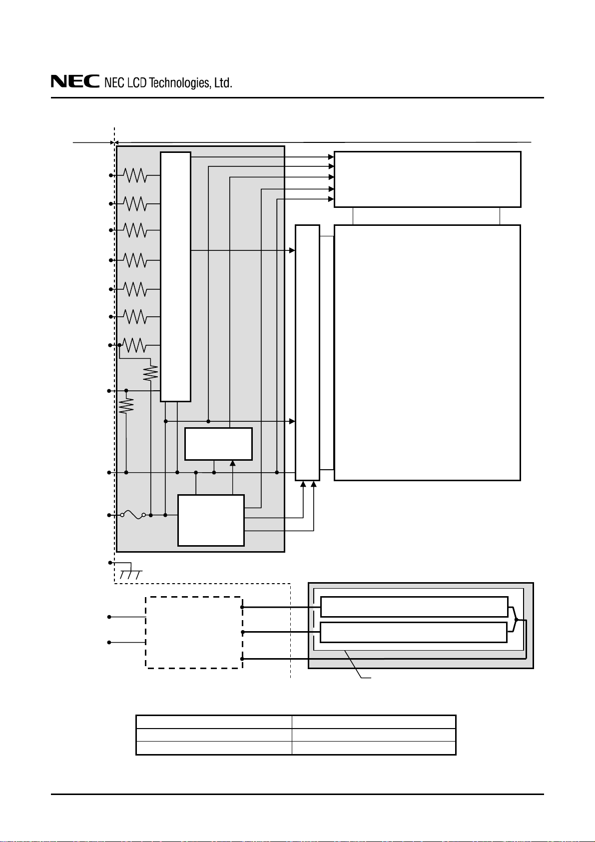
3. BLOCK DIAGRAM
Host
LCD module (Product)
R0 to R5
G0 to G5
B0 to B5
200Ω
200Ω
200Ω
CLK
Hsync
Vsync
DE
47Ω
200Ω
200Ω
200Ω
DPS
GND
Note1
Note2
VCC
Fuse
FG
VDDB
GNDB
Note2
Note1: Relations between GND (Signal ground), FG (Frame ground) and VBLC (Lamp low voltage
terminal) in the LCD module are as follows.
Note2: GND, FG and GNDB must be connected to customer equipment’s ground, and it is
recommended that these grounds are connected together in customer equipment.
NL8060BC31-27/27D
H-driver
2,400 lines
Controller
LCD panel
H: 800 × 3 (R, G, B)
600 lines
Ω
47
Power supply
for gradation
DC/DC
converter
LCD panel signal processing board
V-driver
VBLH
Inverter
(Option)
VBLH
VBLC
Note1
GND-FG Not connected
GND-VBLC Not connected
FG-VBLC Not connected
V: 600
Backlight (Edge light type)
Lamp
Lamp
Metallic frame of lamp holder
DATA SHEET DOD-PP-0214 (8th edition)
6

4. DETAILED SPECIFICATIONS
4.1 MECHANICAL SPECIFICATIONS
Parameter Specification Unit
NL8060BC31-27/27D
Module size
Display area
Weight 740 (typ.), 770 (max.) g
Note1: See "7. OUTLINE DRAWINGS".
4.2 ABSOLUTE MAXIMUM RATINGS
Parameter Symbol Rating Unit Remarks
Power supply
voltage
Input voltage
for signals
Operating temperature
LCD panel signal processing board VCC -0.3 to +6.5 V
Storage temperature Tst -20 to +80
280.0 ± 0.5 (W) × 210.0 ± 0.5 (H) × 13.0 (typ., D)
13.7 (max., D)
246.0 (H) × 184.5 (V)
Lamp voltage VBLH 1,800 Vrms
Display signals
Note1
Function signal
Note2
Front surface TopF -10 to +70
Rear surface TopR -10 to +70
VD
-0.3 to VCC+0.3 V
VF
°C
°C
°C
Note1 mm
Note1 mm
Ta= 25°C
-
Note3
Note4
Relative humidity
Note5
Absolute humidity
Note5
RH
AH
≤ 95
≤ 85
≤ 70
Note6
%
%
g/m3
40 < Ta ≤ 50°C
Note1: Display signals are CLK, Hsync, Vsync, DE, DATA (R0 to R5, G0 to G5, B0 to B5).
Note2: Function signal is DPS.
Note3: Measured at center of LCD panel surface (including self-heat)
Note4: Measured at center of LCD module's rear shield surface (including self-heat)
Note5: No condensation
Note6: Water amount at Ta= 50°C and RH= 85%
Ta ≤ 40°C
Ta > 50°C
DATA SHEET DOD-PP-0214 (8th edition)
7

4.3 ELECTRICAL CHARACTERISTICS
4.3.1 LCD panel signal processing board
Parameter Symbol min. typ. max. Unit Remarks
Power supply voltage VCC
Power supply current ICC
Logic input voltage for
display signals
Input voltage for DPS
signal
High VDH 0.7VCC - VCC V
Low VDL 0 - 0.3VCC V
High VFH 0.7VCC - VCC V
Low VFL 0 - 0.3VCC V
Note1: Checkered flag pattern [by EIAJ ED-2522]
Note2: Pattern for maximum current
NL8060BC31-27/27D
(Ta = 25°C)
3.0 3.3 3.6 V at VCC= 3.3V
4.75 5.0 5.25 V at VCC= 5.0V
-
-
210
Note1
140
Note1
450
Note2
300
Note2
mA at VCC= 3.3V
mA at VCC= 5.0V
CMOS level
DATA SHEET DOD-PP-0214 (8th edition)
8

4.3.2 Backlight lamp
Lamp current
Lamp voltage
NL8060BC31-27/27D
(Ta= 25°C, Note1)
Parameter Symbol min. typ. max. Unit Remarks
at IBL=5.0mArms:
400cd/m
2
Note3, Note4
Note2, Note3
IBL 2.0 5.0 5.5 mArms
VBLH - 570 - Vrms -
Lamp starting voltage
Note2, Note3, Note5, Note8
Lamp oscillation frequency
Note6
970 - - Vrms
VS
1,410 - - Vrms
FO 58 63 68 kHz -
Ta= 25°C
Ta= -10°C
Note1: This product consists of 2 backlight lamps, and these specifications are for each lamp.
Note2: The lamp voltage cycle between lamps should be kept on a same phase. "VS" and "VBLH"
are the voltage value between low voltage side (Cold) and high voltage side (Hot).
Note3: The asymmetric ratio of working waveform for lamps (Power supply voltage peak ratio,
power supply current peak ratio and waveform space ratio) should be less than 5 % (See the
following figure.). If the waveform is asymmetric, DC (Direct current) element apply into the
lamp. In this case, a lamp lifetime may be shortened, because a distribution of a lamp
enclosure substance inclines toward one side between low voltage terminal (Cold terminal)
and high voltage terminal (Hot terminal). When designing the inverter, evaluate asymmetric of
lamp working waveform sufficiently.
Pa
Pb
Sa
0
Sb
|Pa - Pb|
Pb
|Sa - Sb|
Sb
× 100 ≤ 5 %
× 100 ≤ 5 %
Pa: Supply voltage/current peak for positive, Pb: Supply voltage/current peak for negative
Sa: Waveform space for positive part, Sb: Waveform space for negative part.
Note4: Thi s product consists of 2 lamps. 2 lamps are contained in the 1 lamp holder, and both lamps
are connected to 1 low voltage cable. Recommendation lamp current is 5.0mArms typical for
each lamp, and sum of 2 lamps is 10mArms typical. The lamp current should be measured by
high-frequency current meter at the low voltage terminal.
Note5: The inverter should be designed so that the lamp starting voltage can be maintained for more
than 1 second. Otherwise the lamp may not be turned on.
Note6: In case "FO" is not the recommended value, beat noise may display on the screen, because of
interference between "FO" and "1/th". Recommended value of "FO" is as following
1 1
FO = × × (2n-1)
4 th
th: Horizontal cycle (See "4.9.2 Timing characteristics".)
n: Natural number (1, 2, 3 ⋅⋅⋅⋅⋅⋅⋅⋅)
Note7: Method of lamp cable installation may invite fluctuation of lamp current and voltage or
asymmetric of lamp working waveform. When designing method of lamp cable installation,
evaluate the fluctuation of lamp current, voltage and working waveform sufficiently.
DATA SHEET DOD-PP-0214 (8th edition)
9
 Loading...