

DATA SHEET
TFT COLOR LCD MODULE
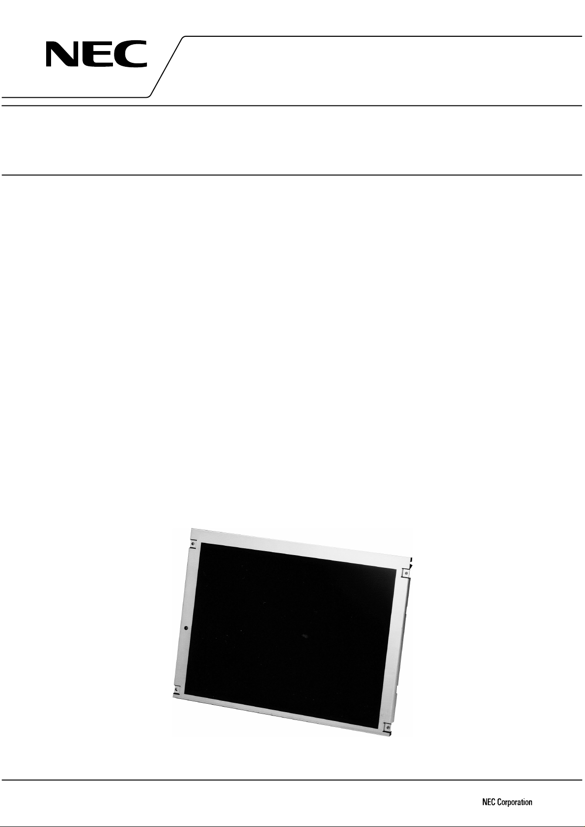
NL8060BC31-17
31 cm (12.1 inches), 800
××××
600 pixels, 262144 colors
High luminance, Wide viewing angle, Reversible scan direction
DESCRIPTION
NL8060BC31-17 is a TFT (thin film transistor) active matrix color liquid crystal display (LCD) module comprising
amorphous silicon TFT attached to each signal electrode, a driving circuit, and a backlight.
NL8060BC31-17 has a built-in backlight. The backlight includes long-life-lamps and the lamps are replaceable
with a holder.
The 31 cm diagonal display area contains 800 × 600 pixels and can display 262144 color simultaneously.
NL8060BC31-17 is suitable for industrial application use, because the viewing angle is wide and the luminance
is high. Also, the viewing direction is selectable either upper or lower side by changing scan direction.
FEATURES
High luminance (350 cd/m
•
Wide viewing angle (with Retardation film)
•
Low reflection
•
Reversible scan direction
•
6-bit digital RGB input signals
•
Data enable (DE) function
•
Smooth polarizer surface (no antiglare treatment)
•
Edge type backlight with two long-life-time lamps (one lamp holder)
•
Lamp holder replaceable
•
2
, at IL= 5mArms/lamp)
APPLICATIONS
Display terminals for control system
•
Monitors for process controller
•
The information in this document is subject to change without notice.
Please confirm with the delivery specification before starting to design the system.
Document No. EN0510EJ1V0DS00
Date Published July 2000 P CP (N)
Printed in Japan
©
2000
NL8060BC31-17
STRUCTURE AND FUNCTIONS
A color TFT (thin film transistor) LCD module is comprised of a TFT liquid crystal panel structure, LSIs for driving
the TFT array, and a backlight assembly. The TFT panel structure is created by sandwiching liquid crystal material
in the narrow gap between a TFT array glass substrate and a color filter glass substrate. After the driver LSIs are
connected to the panel, the backlight assembly is attached to the backside of the panel.
RGB (red, green, blue) data signals from a source system is modulated into a form suitable for active matrix
addressing by the onboard signal processor and sent to the driver LSIs which in turn addresses the individual TFT
cells.
Acting as an electro-optical switch, each TFT cell regulates light transmission from the backlight assembly when
activated by the data source. By regulating the amount of light passing through the array of red, green, and blue
dots, color images are created with clarity.
OUTLINE OF CHARACTERISTICS (at room temperature)
Item Description
Display area 246.0 (H) × 184.5 (V) mm
Drive system a-Si TFT active matrix
Display colors 262,144 colors
Number of pixels 800 × 600 pixels
Pixel arrangement RGB vertical stripe
Pixel pitch 0.3075 (H) × 0.3075 (V) mm
Module size 280.0 (H) × 210.0 (V) × 13.0 (D) mm (typ.)
Weight 750 (typ.)
Contrast ratio 350:1 (typ.)
Viewing angle
(more than the contrast ratio of 10:1)
Designed viewing direction
Color gamut 43% (typ'. at center, to NTSC)
Response time 15 ms (typ.), “white 100%” to ”black 10%”
Luminance
Signal system 6-bit signals for each of RGB primary colors, synchronous signals (Hsync,
Supply voltage 3.3 V [5.0 V] (Logic, LCD driving)
Backlight Edge light type, two cold cathode fluorescent lamp in a holder
Power consumption 7.0 W (typ. at 3.3 V, with a recommended inverter)
Horizontal: 55° (typ. left side, right side)
Vertical: 40° (typ. up side), 50° (typ. down side)
•
Wider viewing angle with contrast ratio : down side
(6 o’clock, normal scan)
up side
(12 o’clock, reverse scan)
•
Wider viewing angle without image reversal: up side
(12 o’clock, normal scan)
down side
(6 o’clock, reverse scan)
•
Optimum grayscale (γ = 2.2) : perpendicular
350 cd/m
Vsync), dot clock (CLK)
•
•
2
(typ.) (Lamp current: IL = 5 mArms per lamp)
Lamp holder : Part No.121LHS15
Recommended invertor: Part No. 121PW111
2
Data Sheet EN0510EJ1V0DS00

BASIC STRUCTURE
NL8060BC31-17
R0 - R5
G0 - G5
B0 - B5
CLK
H sync
V sync
DE
DPS
V
CC
GND
200 Ω
200 Ω
200 Ω
47 Ω
200 Ω
200 Ω
200 Ω
4.7 kΩ
Controller
DC/DC
Converter
Power supply
for drivers
V-driver
H-driver
2400 lines
TFT LCD panel
600 lines
H: 800 × 3 (R, G, B)
V: 600
V
H
V
H
V
L
Note 1:
GND is not connected to FG (Frame Ground) in the LCD module.
Backlight
Backlight
Data Sheet EN0510EJ1V0DS00
3
NL8060BC31-17
GENERAL SPECIFICATIONS
Item Specification Unit
Module size 280.0 ± 0.5 (H) × 210.0 ± 0.5 (V) × 13.7 max. (D) mm
Display area 246.0 (H) × 184.5 (V) [Diagonal display area: 31 cm (Type 12.1)] mm
Number of pixels 800 × 3 (H) × 600 (V) pixel
Dot pitch 0.1025 (H) × 0.3075 (V) mm
Pixel pitch 0.3075 (H) × 0.3075 (V) mm
Pixel arrangement RGB (Red, Green, Blue) vertical stripe
Display colors 262,144 color
Weight 780 (max.) g
ABSOLUTE MAXIMUM RATINGS
Parameter Symbol Rating Unit Remarks
−
Supply voltage V
Input voltage V
Lamp voltage V
Storage temp. T
Operating temp. T
CC
I
L
ST
OP
−
0.3 to 6.5 V
−
0.3 to V
CC
+ 0.3 V
1800 V
−
20 to 60
0 to 50
≤
95 % T
≤
85 % 40 < T
Absolute humidity Absolute humidity shall not
exceed T
a
= 50°C, RH=85%
* Measured at the panel surface (including self-heat)
ELECTRICAL CHARACTERISTICS
(1) Logic LCD driving
Parameter Symbol Min. Typ. Max. Unit Remarks
Supply voltage V
Logic input “L” voltage V
Logic input “H” voltage V
Supply current I
CC
IL
IH
CC
3.0
(4.75)
0
VCC × 0.7
−
−
3.3
(5.0)
−
−
* 320
(240)
g/m
3.6
(5.25)
VCC × 0.3 V
CC
V
600
mA
(500)
rms
°
C
°
C Module surface*
a
≤ 40°CRelative Humidity (RH)
a
≤ 50°C
3
Ta > 50°C
VVCC = 3.3 V
CC
(V
= 5.0 V)
CMOS level
V
CC
= 3.3 V
V
CC
(V
= 5.0 V)
Ta = 25°C
−
No condensation
Ta = 25°C
* Checker flag pattern (in EIAJ ED-2522)
4
Data Sheet EN0510EJ1V0DS00

(2) Backlight
Parameter Symbol Min. Typ. Max. Unit Remarks
NL8060BC31-17
Ta = 25°C
2.0
Lamp current I
Lamp voltage V
Note 2
Oscillator frequency Ft 58 65 69 kHz
Note 1:
In an atmosphere of below 10°C, keep the lamp current more than 3.0 mArms in order to prevent the
L
L
S
V
−
960
1200
Note 1
5.0 5.5 mArm at a lamp
600
−−
−−
−
lamp from blinking.
Note 2:
Note 3:
The phase of the supply voltage for lamps must keep same one.
Recommended value of "Ft".
Ft is within the specification.
•
and
Ft = 1/4th × (2n-1) th: Hsync period
•
n: a natural number (1, 2, 3…)
If Ft is out of the recommended value, interference between Ft frequency and Hsync frequency may
cause beat on the display.
SUPPLY VOLTAGE SEQUENCE
The supply voltage for input signals
should be the same as V
Turn on the backlight within the LCD
2.
operation period. When the backlight
turns on before LCD operation or the
LCD operation turns off before the
backlight turns off, the display may
momentarily become white.
When the power is off, please keep
3.
whole signals (Hsync, Vsync, CLK,
DE, R0-R5, G0-G5, B0-B5) low level
or high impedance.
Wrong power sequence may dam-
4.
age to the module.
The signal should not be down dur-
5.
ing operation. Even if signal could
recover, LCD module can not be
operated correctly, the display may
be un-uniformity. In case signal is
down, V
then turn V
sequence.
3.0 (4.75 V)
CC
V
Signals
V
CC
- ON
Signals: CLK, Hsync, Vsync, DE, R0-R5, G0-G5, B0-B5
0<t<35 ms 0<t<35 ms
VALID
3.0 (4.75 V)
V
CC
- OFF
Notes1.
Time
Vrms I
Vrms
CC
should be turned off, and
CC
and signal on as above
Ta = 25°CLamp turn on voltage
L
= 5mA
Ta = 0°C
Note 3
CC
.
Data Sheet EN0510EJ1V0DS00
5

NL8060BC31-17
INTERFACE AND CONNECTOR PIN ASSIGNMENT
(1) Interface signals, power supply
CN1: DF9-41P-1V (HIROSE ELECTRIC CO., LTD.)
Adaptable socket: DF9-41S-1V (HIROSE ELECTRIC CO., LTD.)
or
IL-310-T41S-VF (Japan Aviation Electronics Industry Limited (JAE)
Pin No. Symbol Function Pin No. Symbol Function
1 GND Ground 22 GND Ground
2 CLK Dot clock 23 G3 Green data
3 GND Ground 24 G4 Green data
4 Hsync Horizontal sync. 25 G5 Green data (MSB)
5 Vsync Vertical sync. 26 GND Ground
6 GND Ground 27 GND Ground
7 GND Ground 28 GND Ground
8 GND Ground 29 B0 Blue data (LSB)
9 R0 Red data (LSB) 30 B1 Blue data
10 R1 Red data 31 B2 Blue data
11 R2 Red data 32 GND Ground
12 GND Ground 33 B 3 Blue data
13 R3 Red data 34 B4 Blue data
14 R4 Red data 35 B5 Blue data (MSB)
15 R5 Red data (MSB) 36 GND Ground
16 GND Ground 37 DE Data enable signal
17 GND Ground 38 N.C. Not Connection
18 GND Ground 39 V
19 G0 Green data (LSB) 40 V
20 G1 Green data 41 DPS
21 G2 Green data
LSB : Least Significant Bit
MSB : Most Significant Bit
CC
CC
Power supply
Power supply
Scan direction select
Note 1
Note 1
Note 2
Notes 1.
Notes 2.
DE/This function recognizes Fixed or DE mode whe Vsync rises.
Low = DE mode
High = Fixed mode
DPS/DPS changes scan direction (normal scan and reverse scan).
Low or Open = Normal scan
High = Reverse scan
See DISPLAY POSITION about the scan directions.
6
Data Sheet EN0510EJ1V0DS00

NL8060BC31-17
(2) Lamp connector
CN2: BHR-03VS-1
Adaptable socket: SM03 (4.0) B-BHS-TB
Supplier: J.S.T TRADING COMPANY, LTD.
Pin No. Symbol Function
1VLLow voltage terminal
2VHHigh voltage terminal
3VHHigh voltage terminal
*VH and VL must be connected correctly. If you make a mistake to connect, you will get hurt and the module
will break.
(3) Connection of recommended Inverter: 121PW111
CN1
Part No.: LZ-5P-SL-SMT
Adaptable socket: LZ-5S-SC3
Supplier: Japan Aviation Electronics Industry Limited (JAE)
Pin No. Symbol Function
1V
2V
3 GNDB Back light ground
4 GNDB Back light ground
5 BRTHL
DDB
DDB
Note 1:
Power supply (12 V)
Power supply (12 V)
Luminance control
Note 1
BRTHL = High (+5 V) or open : High luminance (100%)
BRTHL = Low (GNDB level) : Low luminance (20%)
CN3
Part No.: IL-Z-3PL-SMTY
Adaptable socket: IL-Z-3S-S125C3
Supplier: Japan Aviation Electronics Industry Limited (JAE)
Pin No. Symbol Function
1BRTC
2BRTH
3BRTL
Backlight ON/OFF signal
Luminance control input
Luminance control input
Note 1
Note 2
Note 2
Notes 1.
BRTC = High (+5 V) or Open : Backlight “ON”
BRTC = Low (GNDB level) : Backlight “OFF”
Data Sheet EN0510EJ1V0DS00
7
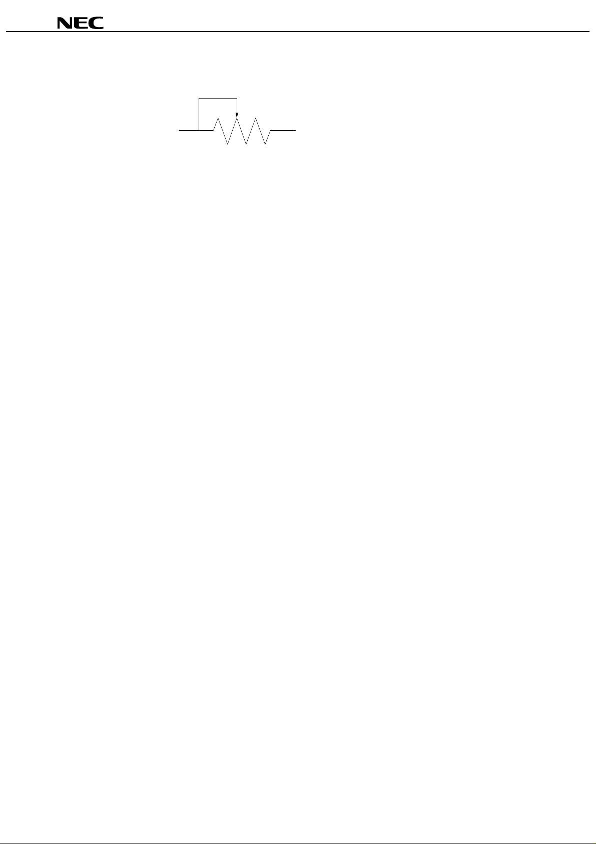
<1> A way of luminance control by a variable resistor.
2.
This way works when BRTHL (No.5 pin) of CN1 is opened.
BRTHBRTL
R
<2> A way of luminance control by a voltage
BRTL and BRTHL are opened. The range of input voltage between BRTH and GNDB is
as follows.
Minimum luminance (20%, typ.) : 3.45 V
Maximum luminance (100%) : ≤ 1.0 V
NL8060BC31-17
Mating variable resistor : 10 kΩ ±5 %
Minimum luminance (20%) : R = 0
Maximum luminance (100%): R = 10 k
Ω
Ω
8
Data Sheet EN0510EJ1V0DS00
 Loading...