

NEC NL6448BC33-31 Datasheet

DATA SHEET
TFT COLOR LCD MODULE
NL6448BC33-31
26 cm (10.4 inches), 640
××××
480 pixels, 262,144 colors,
Incorporated two-lamp/Edge-light type backlight
Wide viewing angle
DESCRIPTION
NL6448BC33-31 is a TFT (thin film transistor) active matrix color liquid crystal display (LCD) comprising
amorphous silicon TFT attached to each signal electrode, a driving circuit and a backlight. NL6448BC33-31 has a
built-in backlight. Backlight includes long-life-lamps and the lamps are replaceable.
The 26 cm (10.4 inches) diagonal display area contains 640 × 480 pixels and can display 262,144 colors
simultaneously.
NL6448BC33-31 is suitable for industrial application use because of the wide viewing angle and the high
luminance. Also, the viewing direction is selectable either upper or lower side by changing scan direction.
NL6448BC33-31 interface is compatible with NL6448AC33-18, -18A, -18B and -27.
FEATURES
• Wide viewing angle (with Retardation Film)
• Smooth polarizer surface (No antiglare treatment)
• High luminance (350 cd/m2, typ.: saturated value, at
room temp.)
• Low reflection
• 6-bit digital RGB signals
• Data enable function
• Backlight with two long-life-time lamps (one lamp
holder, inverter-less)
• Lamp holder replaceable (Type No.: 104LHS31)
• Reversible scan direction (with DPS pin)
• Replaceable lamp holders (Type No.: 104LHS31)
• Recommended inverter (Part No.: 104PWRI)
• Best viewing angle select function (with MVA terminal)
• Luminance control
• Easy to attach a touch panel
APPLICATIONS
• Display terminals for control system
• Monitors for process controller
• Industrial PCs
The information in this document is subject to change without notice.
Document No. EN0443EJ1V0DS00 (1st edition)
Date Published July 1999 P
Printed in Japan
1999©

NL6448BC33-31
STRUCTURE AND FUNCTIONS
A color TFT (thin film transistor) LCD module is comprised of a TFT liquid crystal panel structure, LSIs for driving
the TFT array, and a backlight assembly. The TFT panel structure is created by sandwiching liquid crystal material
in the narrow gap between a TFT array glass substrate and a color filter glass substrate. After the driver LSIs are
connected to the panel, the backlight assembly is attached to the backside of the panel.
RGB (red, green, blue) data signals from a source system is modulated into a form suitable for active matrix
addressing by the onboard signal processor and sent to the driver LSIs which in turn addresses the individual TFT
cells.
Acting as an electro-optical switch, each TFT cell regulates light transmission from the backlight assembly when
activated by the data source. By regulating the amount of light passing through the array of red, green, and blue
dots, color images are created with clarity.
OUTLINE OF CHARACTERISTICS (at room temperature)
Display area 211.2 (H) × 158.4 (V) mm
Drive system a-Si TFT active matrix
Display colors 262,144 colors
Number of pixels 640 × 480 pixels
Pixel arrangement RGB vertical stripe
Pixel pitch 0.33 (H) × 0.33 (V) mm
Module size 243.0 (H) × 185.1 (V) × 10.75 typ. (D) mm
Weight 530 g (typ.)
Contrast ratio 300 : 1 (typ.)
Viewing angle (more than the contrast ratio of 10 : 1)
Horizontal : 50° (typ., left side, right side)
Vertical : 40° (typ., up side), 45° (typ, down side)
Designed viewing direction Wider viewing angle without image reversal: up side (12 o’clock normal scan)
down side (6 o’clock reverse scan)
Wider viewing angle with contrast ratio : down side (6 o’clock normal scan)
up side (12 o’clo ck re vers e scan )
Optimum grayscale (
Polarizer pencil-hardness 2H (Min., at JIS K5400)
Color gamut 43% (typ. at center, to NTSC)
Response time 15 ms (typ.), white to black
Luminance 350 cd/m
Signal system 6-bit digital signals for each of RGB primary colors, synchronous signals
(Hsync, Vsync), dot clock (CLK)
Supply voltages 3.3 V [5.0 V] (Logic, LCD driving), 12.0 V (Backlight)
Backlight Edge light type, two cold cathode fluorescent lamps (cold cathode type)
[Replaceable parts]
Lamp holder: type No.104LHS31
Power consumption 6.8 W (typ., at 3.3 V, 12.0 V)
2
(TYP)
= 2.2) : perpendicular
γ
2
Data Sheet EN0443EJ1V0DS00
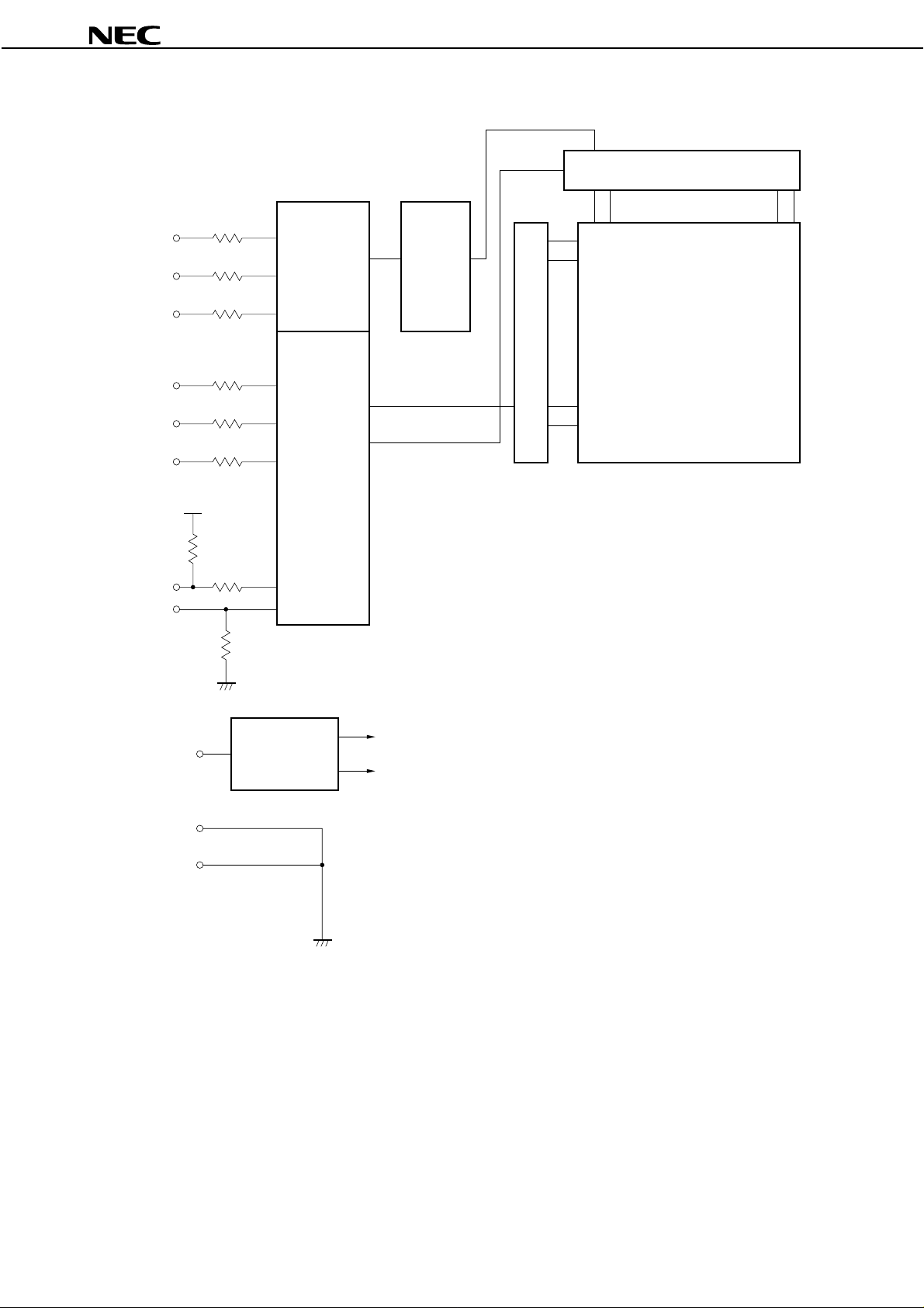
BLOCK DIAGRAM
100 Ω
R0-R5
100 Ω
G0-G5
100 Ω
B0-B5
100 Ω
CLK
100 Ω
H sync
100 Ω
V sync
Digital
signal
processor
LCD timing
controller
Level
shift
·
·
·
·
V-driver
·
· · · · · ·
TFT LCD panel
H: 640 × 3 (R. G. B)
V: 480
480 lines
NL6448BC33-31
H-driver
1920 lines
DE
DPS
V
CC
GND (SG)
Frame (FG)
VCC
47 kΩ
100 Ω
47 kΩ
Power
supply
circuit
LSIs (V
Drivers
CCi
: 3.3 V)
Data Sheet EN0443EJ1V0DS00
3
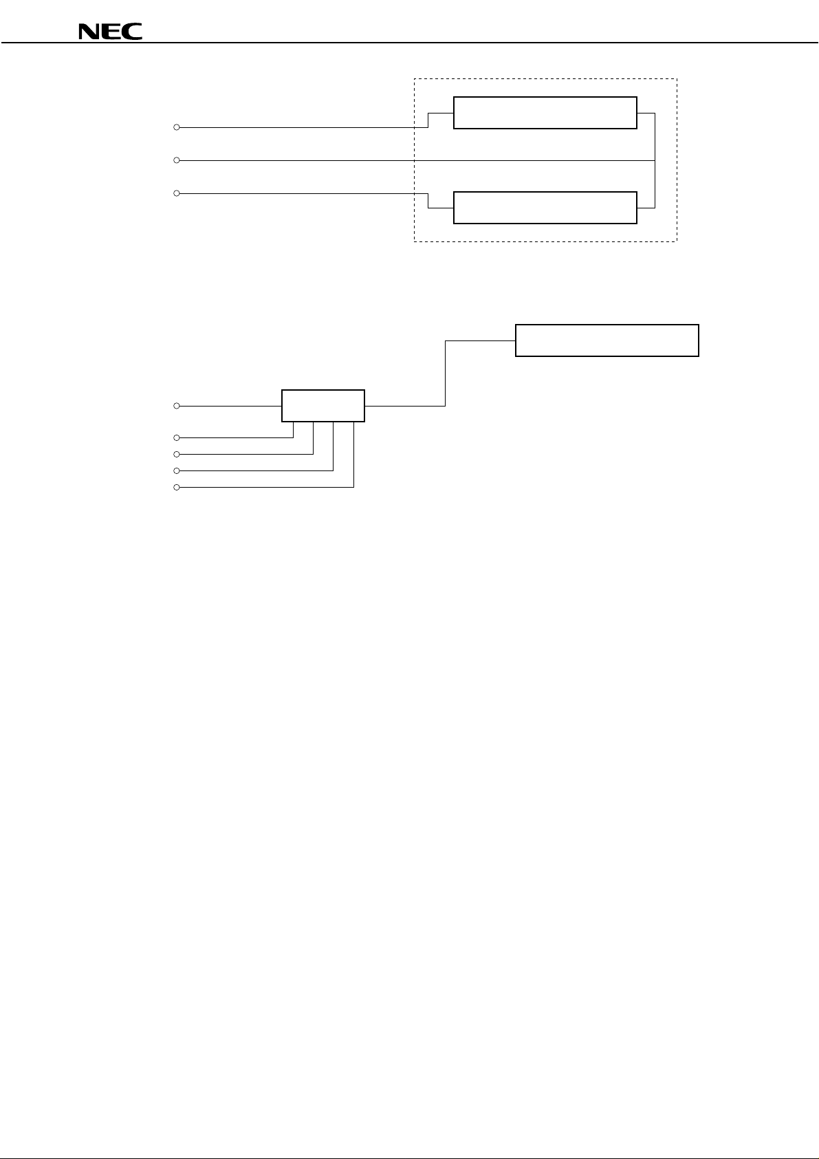
VH
VL
VH
<In case of connecting NEC recommended inverter>
InverterVDDB
BRTC
BRTL
BRTH
GNDB
NL6448BC33-31
Lamp
Lamp
Backlight
Backlight
(Part No. 104PWBR1)
4
Data Sheet EN0443EJ1V0DS00
NL6448BC33-31
GENERAL SPECIFICATIONS
Items Specifications Unit
Module size 243.0 ± 0.5 (H) × 185.1 ± 0.5 (V) × 11.5 max. (D) mm
Display area 211.2 (H) × 158.4 (V) mm
Number of dots 640 × 3 (H) × 480 (V) dot
Number of pixels 640 (H) × 480 (V) pixel
Dot pitch 0.11 (H) × 0.33 (V) mm
Pixel pitch 0.33 (H) × 0.33 (V) mm
Pixel arrangement RGB (Red, Green, Blue) vertical stripe –
Display colors 262,144 color
Weight 550 (max.) g
ABSOLUTE MAXIMUM RATINGS
Parameters Symbols Ratings Unit Remarks
Supply voltage V
Input voltage V
Lamp voltage V
Storage temp. T
Operating temp. T
Humidity
(no condensation)
Measured at the display area
Note
RH
CC
I
L
ST
OP
–0.3 to VCC +0.3 V
≤
95% relative humidity – T
≤
85% relative humidity –
Absolute humidity shall not
exceed T
a
relative humidity level.
–0.3 to 6.5 V
2000 V
–20 to 60
0 to 50
= 50°C, 85%
a
T
= 25°C
rms
°
C
Module surface
°
C
a
≤ 40°C
40 < Ta ≤ 50°C
a
–T
> 50°C
−
Note
No condensation
Data Sheet EN0443EJ1V0DS00
5
ELECTRICAL CHARACTERISTICS
(1) Logic, LCD driving
Parameters Symbols MIN. TYP. MAX. Unit Remarks
NL6448BC33-31
Ta = 25°C
Supply voltage V
Logic input Low voltage V
Logic input High voltage V
Supply current I
Checkered flag pattern (in EIAJ ED-2522)
Note
(2) Backlight
Parameters Symbols MIN. TYP. MAX. Unit Remarks
Lamp current I
Lamp voltage V
Oscillator frequency F
Recommended value of “F
Note
•Ft is within the specification.
CC
IL
IH
CC
L
L
S
t
3.0
(4.75)
0–V
VCC × 0.7 – 5.25 V
–
–
2.0 5.0 5.5 mArms with one lamp
−
840
1265
50 54 58 kHz
t
”.
3.3
(5.0)
325
Note
(250)
510
−−
−−
3.6
(5.25)
CC
× 0.3 mV
370
(300)
−
VVCC = 3.3 V
CC
= 5.0 V)
(V
CMOS level
mA VCC = 3.3 V
CC
= 5.0 V)
(V
Vrms
Vrms
a
T
= 25°CLamp turn on voltage V
Ta = 0°C
Note
a
= 25°C
T
−
and
1
Ft =
•
4th
× (2n – 1)
If Ft is out of the recommended value, interference between Ft frequency and Hsync frequency may cause
beat on the display.
SUPPLY VOLTAGE SEQUENCE
Signals
Backlight
V
Notes 1, 2, 3
Note 4
3.0 V (4.75 V)
CC
0 V
0 V
0 < t < 35 ms 0 < t < 35 ms
ON OFF
thn: Hsync period
: a natural number (1, 2, 3, ····)
3.0 V (4.75 V)
VALID
2tV < t
0 < t
Time
otes 1.
Signals: CLK, Hsync, Vsync, DE,
DATA (R0-R5, G0-G5, B0-B5)
The supply voltage for input signals
2.
CC
should be the same as V
Apply VDDB within the LCD operation
3.
.
period. When the backlight turns on
before LCD operation or the LCD
operation turns off before the backlight
turns off, the display may momentarily
become white.
While the power is off, please keep
4.
whole signals at low level or high
impedance.
6
Data Sheet EN0443EJ1V0DS00
NL6448BC33-31
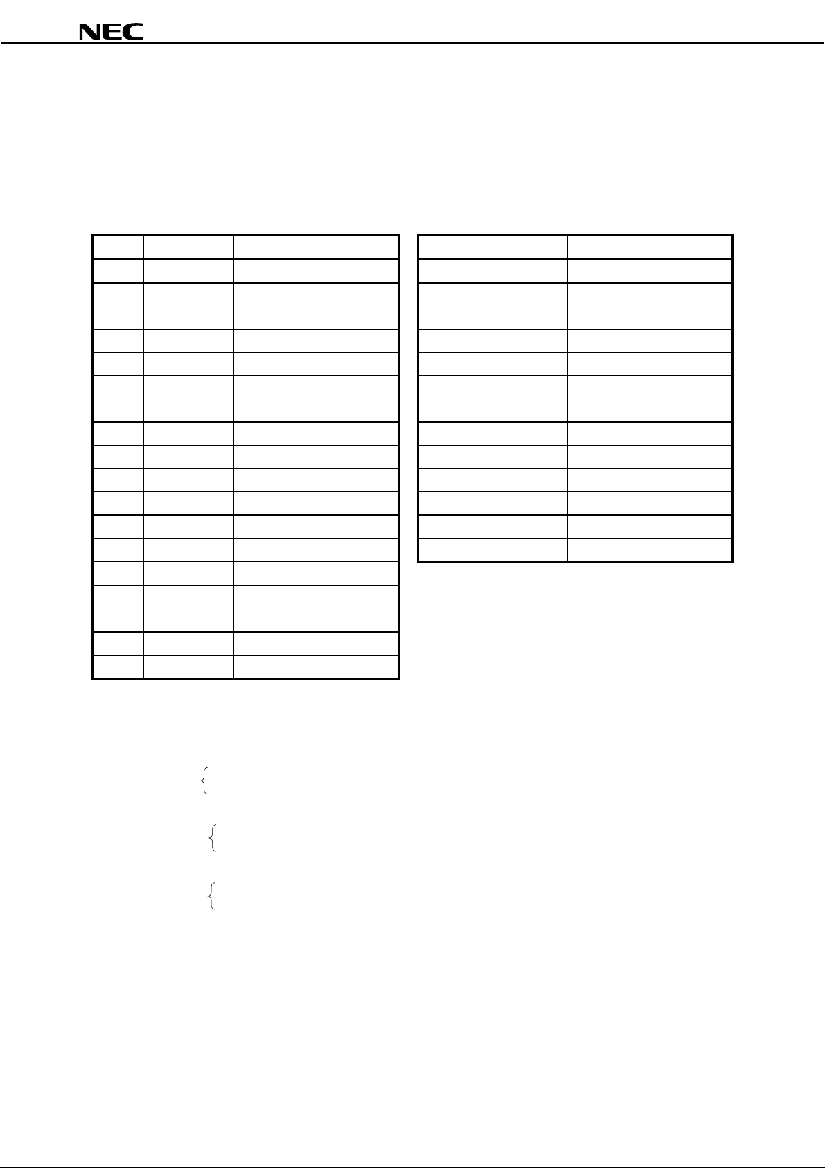
INTERFACE PIN CONNECTIONS
(1) Interface signals, power supply
Module side connector Mating connector
CN1 ··· DF9C-31P-1V (No.1 to 30) DF9-31S-1V or DF9M-31S-1R ...... (1)
IL-310-T31S-VF ...... (2)
Supplier: (1) HIROSE ELECTRIC CO., LTD., (2) Japan Aviation Electronics Industry Limited (JAE)
Pin No. Symbols Functions Pin No. Symbols Functions
1 GND Ground 19 GND Ground
2 CLK Dot clock 20 B0 Blue data (LSB)
3 Hsync Horizontal sync. 21 B1 Blue data
4 Vsync Vertical sync. 22 B2 Blue data
5 GND Ground 23 B3 Blue data
6 R0 Red data (LSB) 24 B4 Blue data
7 R1 Red data 25 B5 Blue data (MSB)
8 R2 Red data 26 GND Ground
9 R3 Red data 27 DE Data enable
10 R4 Red data 28 V
11 R5 Red data (MSB) 29 V
12 GND Ground 30 MVA Best Viewing Select
13 G0 Green data (LSB) 31 DPS Scan direction select
CC
CC
Power supply
Power supply
14 G1 Green data
15 G2 Green data
16 G3 Green data
17 G4 Green data
18 G5 Green data (MSB)
CC
: All VCC terminals should be connected to 3.3V or 5.0 V.
Notes 1.
V
GND is connected to the frame of the LCD module.
2.
DE: DE/Fixed mode select is as follows.
3.
Data enable signal = DE mode
CC
or Open = Fixed mode
V
MVA: MVA changes best viewing angle at gray scale screen.
4.
CC
or Open = Perpendiculer (best viewing angle: 0°)
V
GND = down side (best viewing angle: −10°)
DPS: DPS changes display scan direction.
5.
GND or Open = Scan direction will be decided by the setting of SW1.
CC
= Reverse scan
V
DISPLAY POSITION about another way for reversible scan.
CC
When DPS is V
, reverse scan is selected even if SW1 is set at normal scan.
LSB : Least Significant Bit
MSB : Most Significant Bit
Data Sheet EN0443EJ1V0DS00
7
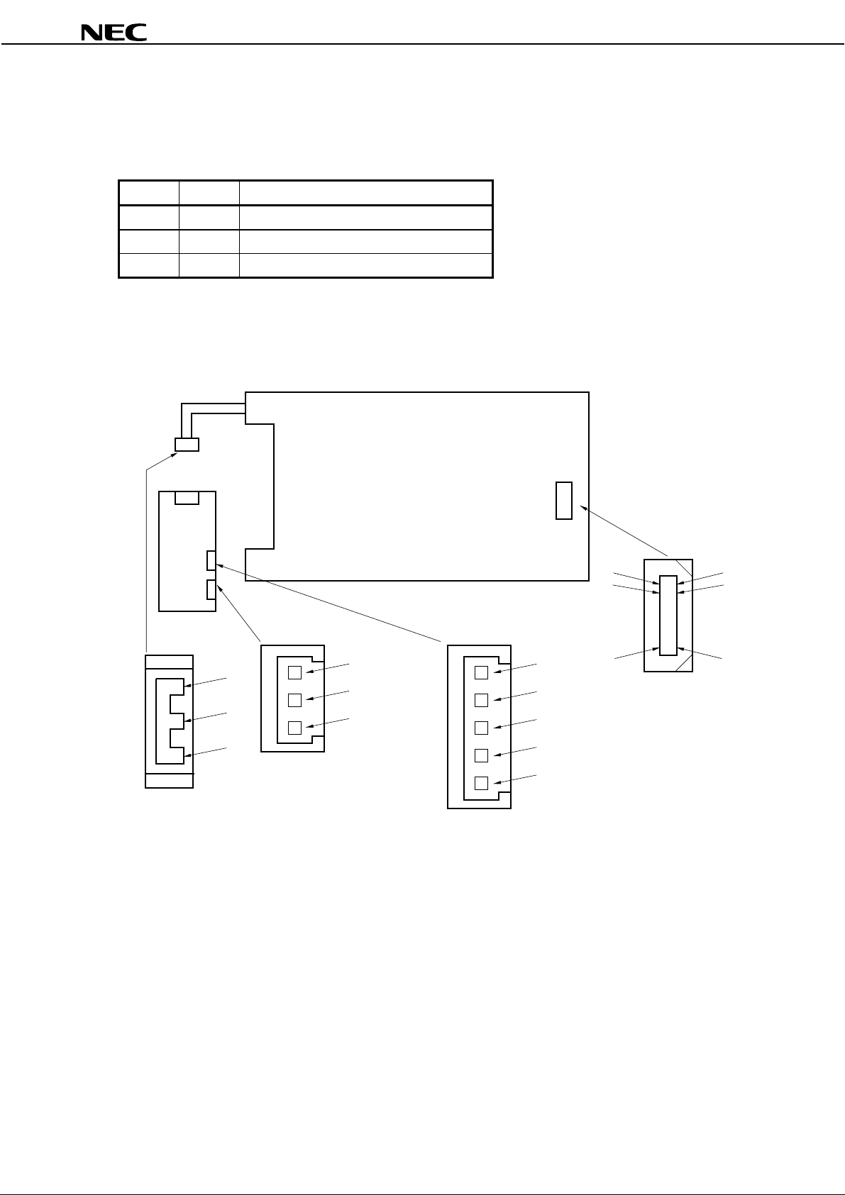
(2) Backlight
• Lamp side connector Mating connector
CN2 ··· BHR-03VS-1 SM03 (4.0)B-BHS-TB
Supplier: J.S.T TRADING COMPANY, LTD.
Pin No. Symbols Func tions
NL6448BC33-31
1V
2V
3V
L
H
H
(3) Connector locations
<Connector locations>
CN2
NEC
Recommended
inverter
CN1
CN3
Power supply (low)
Power supply (high)
Power supply (high)
1
2
1
2
3
Upper side
LCD Module
<Rear view>
Lower side
CN1
1
3
•
•
•
•
•
1
2
3
31
<Pin arrangement of CN1>
2
4
•
•
•
•
•
30
3
<Pin arrangement of CN3>
<Pin arrangement of CN2>
Incase of connecting NEC recommended inverter
8
4
5
<Pin arrangement of CN1>
Data Sheet EN0443EJ1V0DS00
 Loading...