

NEC NL204153BM21-01A Specification

TFT MONOCHROME LCD MODULE
NL204153BM21-01
NL204153BM21-01A
54.0cm (21.3 Type)
QXGA
LVDS Interface (4 ports)
DATA SHEET
DOD-PD-0556 (2nd edition)
This DATA SHEET is updated document from
DOD-PD-0521(1).
All information is subject to change without notice.
Please confirm the sales representative before
starting to design your system.
Document Number: DOD-PD-0556 (2nd edition)
Published date: June 2004 CP(N)
1
© NEC LCD Technologies, Ltd.
2004 All rights reserved.

NL204153BM21-01/-01A
INTRODUCTION
No part of this document shall be copied in any form or by any means without the prior written consent
of NEC Corporation.
NEC Corporation does not assume any liability for infringement of patents, copyrights or other
intellectual property rights of third parties by or arising from use of a product described herein or any
other liability arising from use of such application. No license, express, implied or otherwise, is granted
under any patents, copyrights or other intellectual property rights of NEC Corporation or of others.
While NEC Corporation has been making continuous effort to enhance the reliability of its products, the
possibility of failures cannot be eliminated entirely. To minimize risks of damage to property or injury to
person arising from a failure in an NEC product, customers must incorporate sufficient safety measures in
their design, such as redundancy, fire-containment and anti-failure features.
NEC products are classified into the following three quality grades:
"Standard", "Special", "Specific"
The "Specific" quality grade applies only to applications developed based on a customer designated
"quality assurance program" for a specific application. The recommended applications of a product
depend on its quality grade, as indicated below. Customers must check the quality grade of each
application before using it in a particular application.
Standard: Computers, office equipment, communications equipment, test and measurement equipment,
audio and visual equipment, home electronic appliances, machine tools, personal electronic
equipment and industrial robots
Special: Transportation equipment (automobiles, trains, ships, etc.), traffic control systems, anti-disaster
systems, anti-crime systems, safety equipment and medical equipment (not specifically
designed for life support)
Specific: Military systems, aircraft, aerospace equipment, submersible repeaters, nuclear reactor control
systems, life support systems (medical equipment, etc.) and any other equipment
The quality grade of this product is "Standard" unless otherwise specified in this document. If
customers intend to use this product for applications other than those specified for "Standard" quality
grade, they should contact NEC Corporation sales representative in advance.
DATA SHEET DOD-PD-0556 (2nd edition)
2

NL204153BM21-01/-01A
CONTENTS
INTRODUCTION ..........................................................................................................................................2
1. OUTLINE....................................................................................................................................................4
1.1 STRUCTURE AND PRINCIPLE...........................................................................................................4
1.2 APPLICA TION.......................................................................................................................................4
1.3 FEATURES.............................................................................................................................................4
2. GENERAL SPECIFICATIONS ................................................................................................................5
3. BLOCK DIAGRAM...................................................................................................................................6
4. DETAILED SPECIFICATIONS...............................................................................................................7
4.1 MECHANICAL SPECIFICATIONS......................................................................................................7
4.2 ABSOLUTE MAXIMUM RATINGS....................................................................................................7
4.3 ELECTRICAL CHARACTERISTICS...................................................................................................8
4.3.1 LCD panel signal processing board...............................................................................................8
4.3.2 Backlight lamp...............................................................................................................................9
4.3.3 Power supply voltage ripple.........................................................................................................10
4.3.4 Fuse..............................................................................................................................................10
4.4 POWER SUPPLY VOLTAGE SEQUENCE........................................................................................11
4.5 CONNECTIONS AND FUNCTIONS FOR INTERFACE PINS.........................................................12
4.5.1 LCD panel signal processing board.............................................................................................12
4.5.2 Backlight lamp.............................................................................................................................14
4.5.3 Positions of plug and socket ........................................................................................................16
4.6 METHOD OF CONNECTION FOR LVDS TRANSMITTER............................................................17
4.7 DISPLAY GRAY SCALE AND INPUT DATA SIGNALS..................................................................19
4.8 INPUT SIGNAL TIMINGS..................................................................................................................20
4.8.1 Timing characteristics..................................................................................................................20
4.8.2 Input signal timing chart..............................................................................................................20
4.9 LVDS DATA TARANSMISSION METHOD ......................................................................................21
4.10 DISPLAY POSITIONS.......................................................................................................................21
4.11 PIXEL ARRANGNMENT.........................................................................................................
4.12 TEN-bit LOOK UP TABLE FOR GAMMA ADJUSTMENT............................................................23
4.13 LUT SERIAL COMMUNICATION TIMINGS.................................................................................26
4.14 OPTICS...............................................................................................................................................28
4.14.1 Optical characteristics................................................................................................................28
4.14.2 Definition of contrast ratio.........................................................................................................30
4.14.3 Definition of luminance uniformity...........................................................................................30
4.14.4 Definition of response times......................................................................................................30
4.14.5 Definition of viewing angles......................................................................................................30
5. RELIABILITY TESTS.............................................................................................................................31
6. PRECAUTIONS .......................................................................................................................................32
6.1 MEANING OF CAUTION SIGNS......................................................................................................32
6.2 CAUTIONS..........................................................................................................................................32
6.3 A TTENTI ONS......................................................................................................................................32
6.3.1 Handling of the product...............................................................................................................32
6.3.2 Environment.................................................................................................................................33
6.3.3 Characteristics..............................................................................................................................33
6.3.4 Other............................................................................................................................................33
7. OUTLINE DRAWINGS...........................................................................................................................34
7.1 FRONT VIEW......................................................................................................................................34
7.2 REAR VIEW ........................................................................................................................................35
.........22
DATA SHEET DOD-PD-0556 (2nd edition)
3
1. OUTLINE
1.1 STRUCTURE AND PRINCIPLE
Monochrome LCD module NL204153BM21-01 and NL204153BM21-01A are composed of the
amorphous silicon thin film transistor liquid crystal display (a-Si TFT LCD) panel structure with driver
LSIs for driving the TFT (Thin Film Transistor) array and a backlight.
The a-Si TFT LCD panel structure is injected liquid crystal material into a narrow gap between the TFT
array glass substrate and a monochrome-filter glass substrate.
Grayscale data signals from a host system (e.g. PC, signal generator, etc.) are modulated into best form
for active matrix system by a signal processing board, and sent to the driver LSIs which drive the
individual TFT arrays.
The TFT array as an electro-optical switch regulates the amount of transmitted light from the backlight
assembly, when it is controlled by data signals. Monochrome images are created by regulating the
amount of transmitted light through the TFT array.
1.2 APPLICATION
• Monochrome monitor system
1.3 FEATURES
• Ultra-wide viewing angle (Adoption of Super Advanced -Super Fine TFT (SA-SFT))
• High luminance
• High contrast
• Low reflection
• High resolution
• 256 gray scales per 1 sub-pixel
• LVDS interface
• Adjustable gamma characteristics by using built-in 10-bit LUT (look up table)
• Selectable LVDS data input map
• Small foot print
• Incorporated edge light type backlight (without inverter)
• Replaceable backlight
• Differences between NL204153BM21-01 and NL204153BM21-01A
NL204153BM21-01/-01A
☆
Item NL204153BM21-01 NL204153BM21-01A
White chromaticity Wx, Wy = (0.255, 0.310) (typ.) Wx, Wy = (0.280, 0.304) (typ.)
Luminance 700cd/m
Backlight unit
(Replaceable part)
Cable color of backlight lamps See "4.5.2 Backlight lamp".
2
(min.) 650cd/m2 (min.)
213LHS06 213LHS11
DATA SHEET DOD-PD-0556 (2nd edition)
4
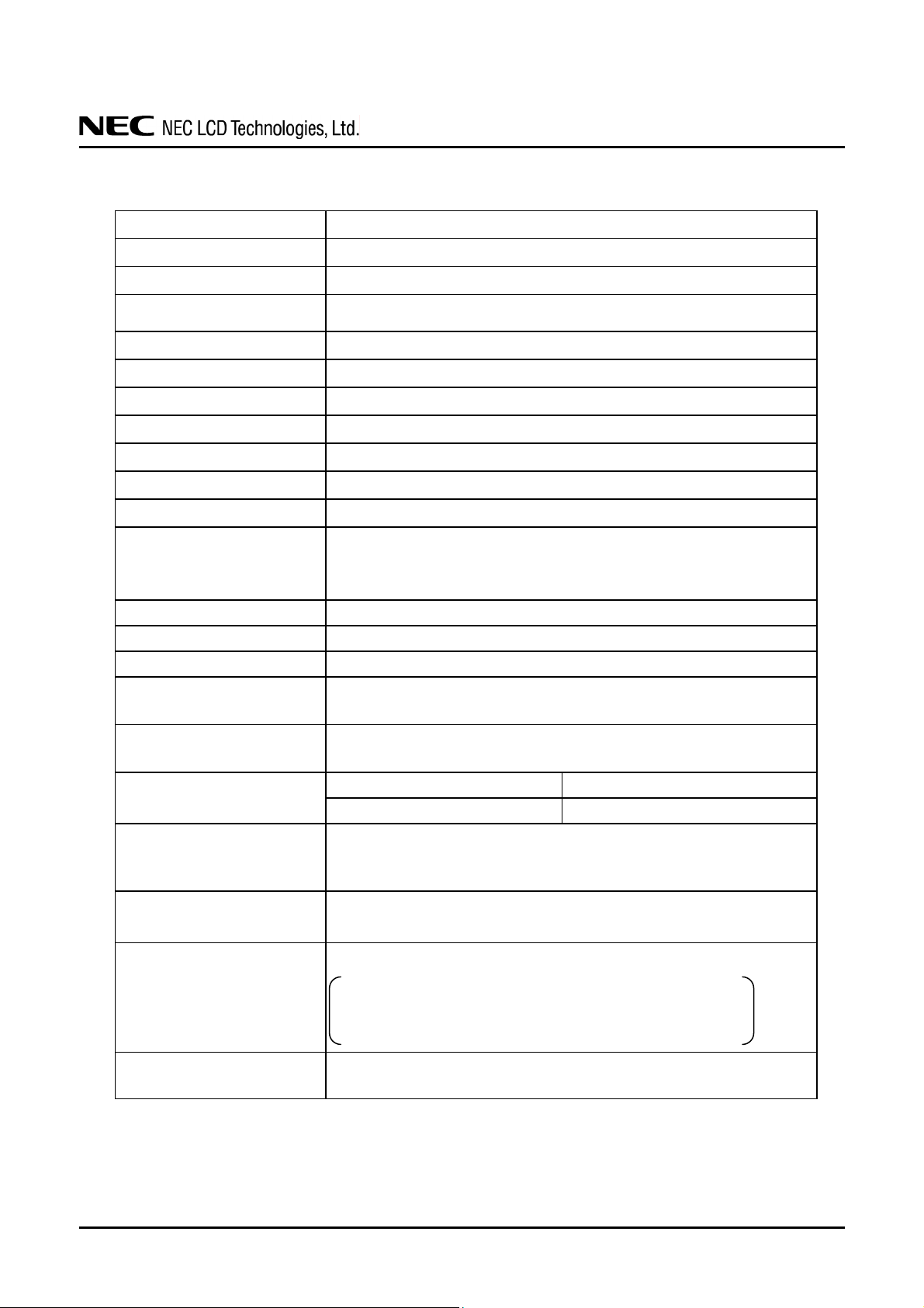
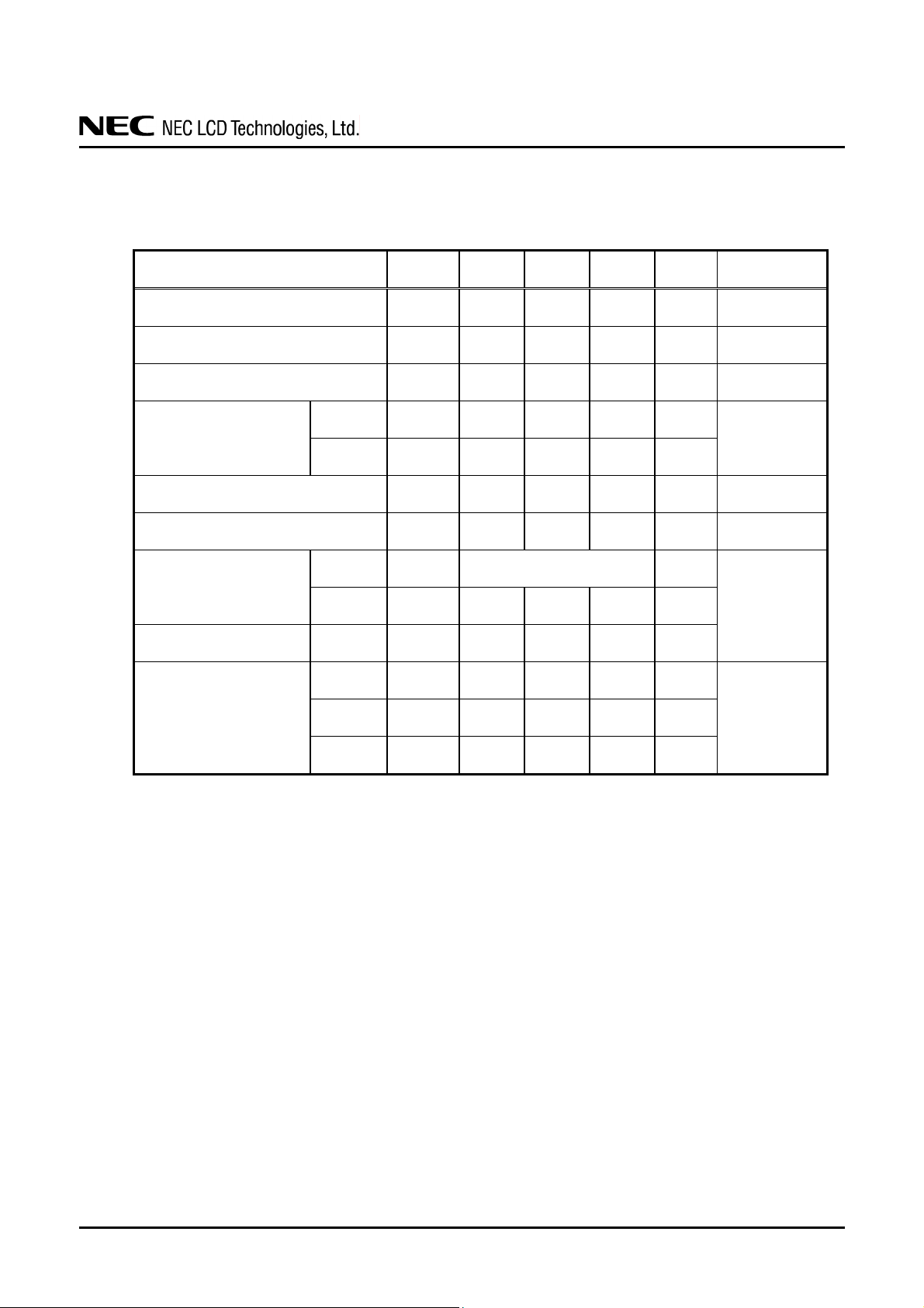
2. GENERAL SPECIFICATIONS
Display area
NL204153BM21-01/-01A
433.152 (H) × 324.864 (V) mm
Diagonal size of display
Drive system
Display grayscale
Pixel
Pixel arrangement
Sub-pixel pitch
Pixel pitch
Module size
Weight
Contrast ratio
Viewing angle
Designed viewing direction
Polarizer surface
Polarizer pencil-hardness
Response time
54.0 cm (21.3 inches)
a-Si TFT active matrix
256 gray scales per 1 sub-pixel (8-bit)
(766 gray scales per 1 pixel)
2,048 (H) × 1,536 (V) pixels (1 pixel consi s ts of 3 sub-pixels (LCR).)
LCR vertical stripe
0.0705 (H) × 0.2115 (V) mm
0.2115 (H) × 0.2115 (V) mm
457.0 (W) × 350.0 (H) × 25.0 (D) mm (typ.)
3,800 g (typ.)
700:1 (typ.)
At the contrast ratio ≥ 10:1
• Horizontal: Right side 85° (typ.), Left side 85° (typ.)
• Vertical: Up side 85° (typ.), Down side 85° (typ.)
Viewing angle with optimum grayscale (γ=DICOM): normal axis Note1
Antiglare
2H (min.) [by JIS K5400]
←→
Ton+Toff (10%
90%)
35 ms (typ.)
Luminance
White chromaticity
At IBL= 6.0mArms / lamp
800 cd/m
NL204153BM21-01 Wx, Wy = (0.255, 0.310) (typ.)
NL204153BM21-01A Wx, W y = (0.280, 0.304) (typ.)
4 ports LVDS interface (THC63LVD824×2 pcs, THine Electronics, Inc. or
Signal system
equivalent)
LCR 8-bit signals, Data enable signal (DE), Dot clock (CLK)
Power supply voltage
LCD panel signal processing board: 12.0V
Edge light type: 6 cold cathode fluorescent lamps (without inverter)
Backlight
Power consumption
Replaceable part
• Backlight unit: Type No. 213LHS06 for NL204153BM21-01
At checkered flag pattern and IBL= 6.0mArms / lamp
34.2 W (typ.)
Note1: When the product luminance is 800cd/m
2
(typ.)
213LHS11 fo r NL204153BM21-01A
2
, the gamma characteristic is designed to γ=DICOM.
DATA SHEET DOD-PD-0556 (2nd edition)
5
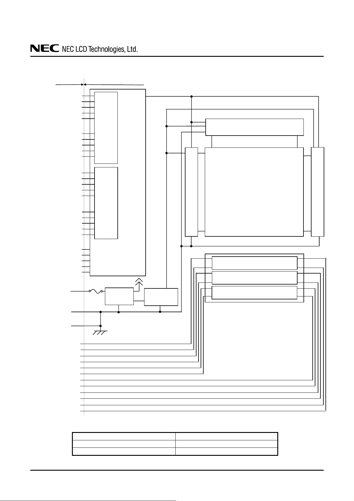
3. BLOCK DIAGRAM
I/F LCD module (Product)
DA0+/–
DA1+/–
DA2+/–
CKA+/–
DA3+/–
DB0+/–
DB1+/–
DB2+/–
CKB+/–
DB3+/–
DC0+/–
DC1+/–
DC2+/–
CKC+/–
DC3+/–
DD0+/–
DD1+/–
DD2+/–
CKD+/–
DD3+/–
CS
SCLK
SDAT
BSEL0
BSEL1
VDD
GND
Note1, Note2
FG
Note1, Note2
VBLH
VBLC
Note1
Note1: Connections between GND (Signal ground), FG (Frame ground) and VBLC (Lamp low voltage
terminal) in the LCD module
GND - FG Connected
GND - VBLC Not connected
FG - VBLC Not connected
Note2 GND and FG must be connected to customer equipment's ground, and it is recommended that GND,
FG and customer inverter ground are connected together in customer equipment.
Fuse
Equivalent of
THC63LVD824 (THine)
Equivalent of
THC63LVD824 (THine)
DC/DC
Converter
Controller
1,536 lines
V-driver
Power supply
for drivers
DATA SHEET DOD-PD-0556 (2nd edition)
NL204153BM21-01/-01A
H-driver
6,144 lines
TFT LCD panel
H: 2,048 × 3 (L, C, R)
V: 1,536
Lamp
Lamp
Lamp
Backlight
(Edge light type)
V-driver
6
4. DETAILED SPECIFICATIONS
4.1 MECHANICAL SPECIFICATIONS
Parameter Specification Unit
NL204153BM21-01/-01A
Module size
Display area
Weight 3,800 (typ.), 4,000 (max.) g
457.0 ± 0.5 (W) × 350.0 ± 0.5 (H) ×
433.152 (H) × 324.864 (V)
25.0±0.5 (D)
Note1, Note2 mm
Note2 mm
Note1: Excluding warpage of the signal processing board cover and the connection board cover.
Note2: See "7. OUTLINE DRAWINGS".
4.2 ABSOLUTE MAXIMUM RATINGS
Parameter Symbol Rating Unit Remarks
Power supply
voltage
Operating temperature
LCD panel signal processing board VDD -0.3 to +14.0 V
Lamp voltage VBLH 2,000 Vrms
Input signal voltage
Note1
Storage temperature Tst -20 to +60 °C -
Front surface TopF 0 to +55 °C Note2
Rear surface TopR 0 to + 60 °C Note3
Vi -0.3 to +2.8 V
Ta = 25°C
Ta = 25°C
VDD=12.0V
≤ 95 % Ta ≤ 40°C
Relative humidity
Note4
Absolute humidity
Note4
RH
AH
≤ 85 % 40 < Ta ≤ 50°C
≤ 70 % 50 < Ta ≤ 55°C
≤ 73
Note5
3
g/m
Ta > 55°C
Note1: DA0+/-, DA1+/-, DA2+/-, DA3+/-, CKA+/-, DB0+/-, DB1+/-, DB2+/-, DB3+/-, CKB+/-, DC0+/-,
DC1+/-, DC2+/-, DC3+/-, CKC+/-, DD0+/-, DD1+/-, DD2+/-, DD3+/-, CKD+/-,
CS, SCLK, SDAT, BSEL0, BSEL1
Note2: Measured at center of LCD panel surface (including self-heat)
Note3: Measured at center of LCD module's rear shield surface (including self-heat)
Note4: No condensation
Note5: Water amount at Ta = 55°C and RH = 70%
DATA SHEET DOD-PD-0556 (2nd edition)
7
4.3 ELECTRICAL CHARACTERISTICS
4.3.1 LCD panel signal processing board
Parameter Symbol min. typ. max. Unit Remarks
Supply voltage VDD 10.8 12.0 13.2 V -
NL204153BM21-01/-01A
(Ta = 25°C)
Supply current IDD -
Ripple voltage VRP - - 100 mVp-p for VDD
Differential input threshold
voltage
Input voltage swing VI 0 - 2.4 V Note4
Terminating resistance RT - 100 -
Control signal input
threshold voltage
Control signal input current Low IIL -10 - 10
Serial communication signal
input threshold voltage
High VTH - - +100 mV
Low VTL -100 - - mV
High VIH High must be Open. -
Low VIL 0 - 0.5 V
High V+ - 1.4 1.9 V
Low V- 0.4 0.7 - V
Hysteresis VH 0.3 - - V
600
Note1
1,100
Note2
mA at VDD=12.0V
at VCM= 1.2V
Note3, Note4
Ω
µA
-
Note5
Note6
Note1: Checkered flag pattern (by EIAJ ED-2522)
Note2: Pattern for maximum current
Note3: Common mode voltage for LVDS driver
Note4: DA0+/-, DA1+/-, DA2+/-, DA3+/-, CKA+/-, DB0+/-, DB1+/-, DB2+/-, DB3+/-, CKB+/-,
DC0+/-, DC1+/-, DC2+/-, DC3+/-, CKC+/-, DD0+/-, DD1+/-, DD2+/-, DD3+/-, CKD+/Note5: BSEL0, BSEL1
Note6: CS, SCLK, SDAT
☆
DATA SHEET DOD-PD-0556 (2nd edition)
8
NL204153BM21-01/-01A
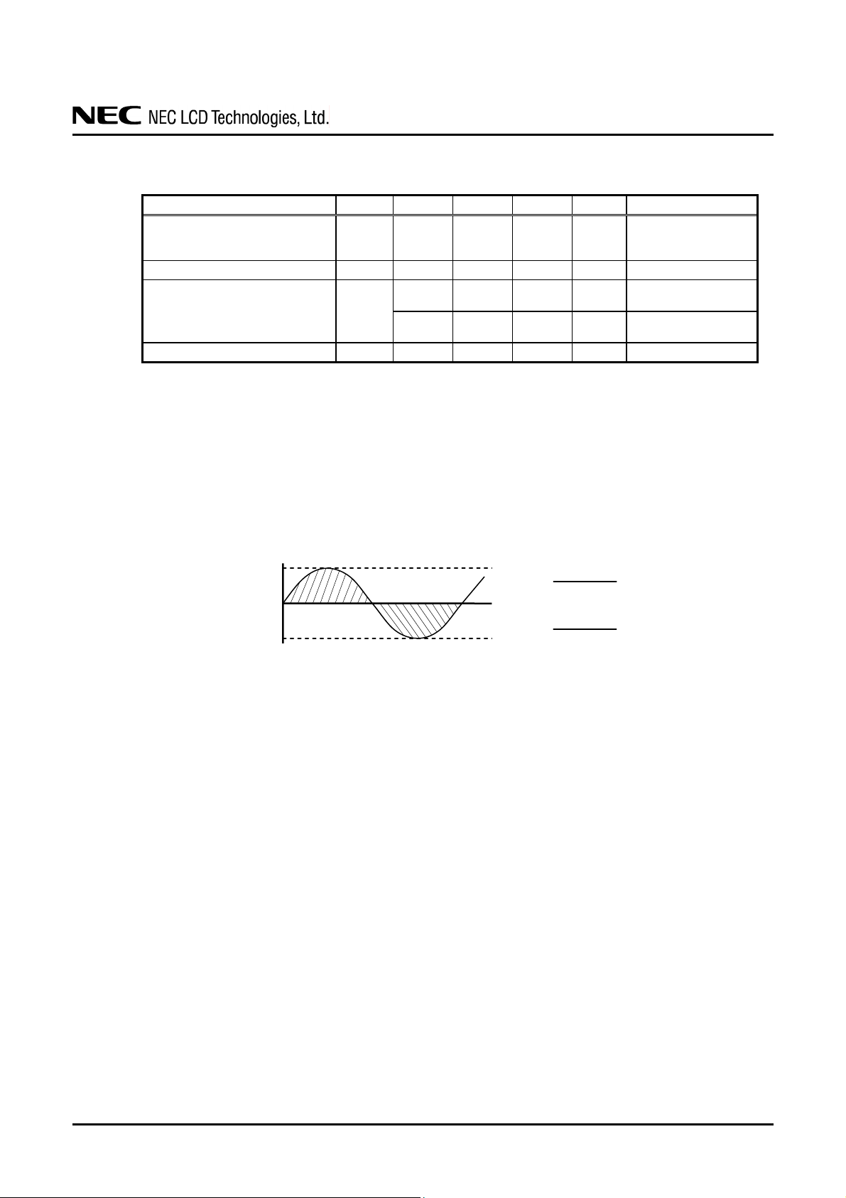
4.3.2 Backlight lamp
Parameter Symbol min. typ. max. Unit Remarks
Lamp current IBL 3.0 6.0 7.0 mArms
Lamp voltage VBLH - 750 - Vrms Note2, Note3
1,220 - - Vrms
Lamp starting voltage VS
1,460 - - Vrms
Lamp oscillation frequency FO 50 58 60 kHz Note4
Note1: This product consists of 6 backlight lamps, and these specifications are for each lamp.
Note2: The lamp voltage cycle between lamps should be kept on a same phase. "VS" and "VBLH" are
the voltage value between low voltage side (Cold) and high voltage side (Hot).
Note3: The asymmetric ratio of working waveform for lamps (Lamp voltage peak ratio, Lamp current
peak ratio and waveform space ratio) should be less than 5 % (See the following figure.). If the
waveform is asymmetric, DC (Direct current) element apply into the lamp. In this case, a lamp
lifetime may be shortened, because a distribution of a lamp enclosure substance inclines
toward one side between low voltage terminal (Cold terminal) and high voltage terminal (Hot
terminal).
Pa: Supply voltage/current peak for positive, Pb: Supply voltage/current peak for negative
Sa: Waveform space for positive part, Sb: Waveform space for negative part.
Note4: A beat noise by interference of "FO" and "1/th" may appear on the screen. (th: Horizontal
cycle (See "4.8.1 Timing characteristics".)) Set up the "FO" so that the beat noise does not
appear.
Note5: Method of lamp cable installation may invite fluctuation of lamp current and voltage or
asymmetric of lamp working waveform. When designing method of lamp cable installation,
evaluate the fluctuation of lamp current, voltage and working waveform sufficiently.
Pa
Pb
Sa
0
Sb
|Sa - Sb|
Pb
Sb
× 100 ≤ 5 %
× 100 ≤ 5 %
|Pa - Pb|
(Ta=25°C, Note1)
at IBL= 6.0mArms:
800 cd/m
Ta = 25°C
Note2, Note3
Ta = 0°C
Note2, Note3
Note3
2
DATA SHEET DOD-PD-0556 (2nd edition)
9
NL204153BM21-01/-01A
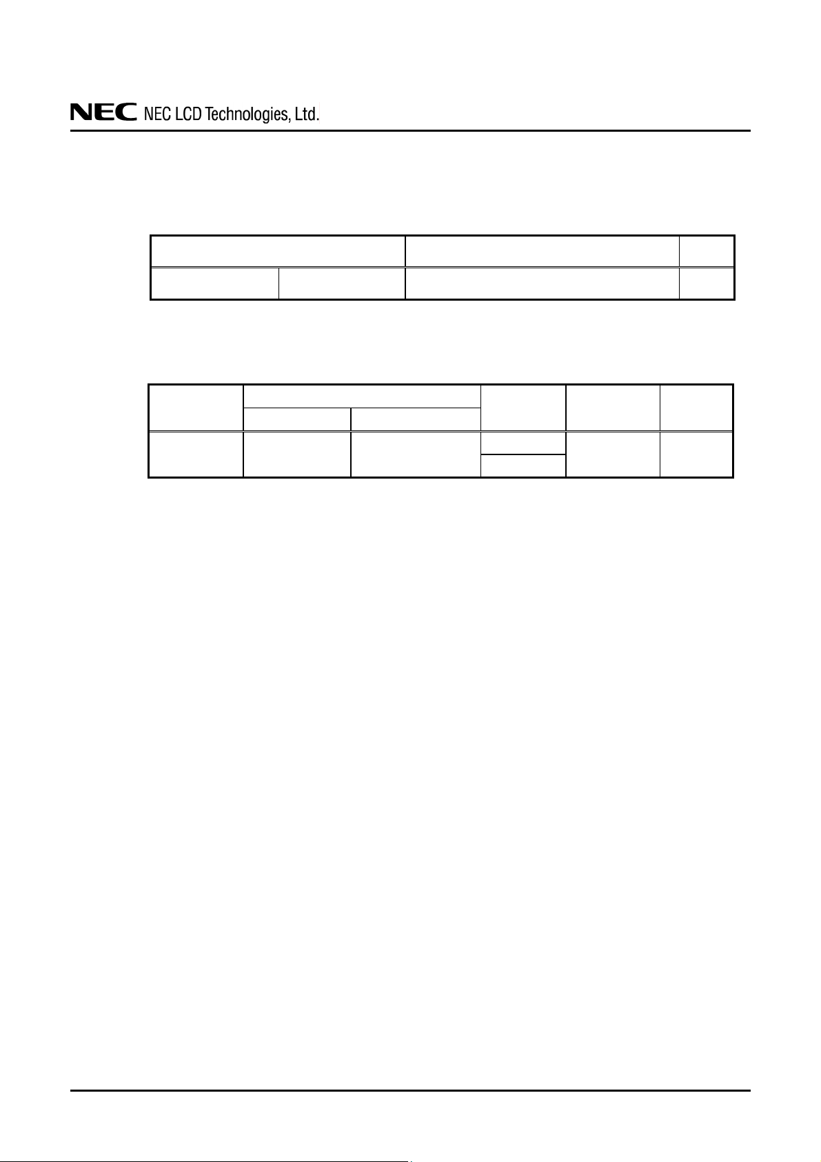
4.3.3 Power supply voltage ripple
This product works, even if the ripple voltage levels are beyond the permissible values as following
the table, but there might be noise on the display image.
Power supply voltage
(Measure at input terminal of power supply)
Ripple voltage Note1
Unit
Note1: The permissible ripple voltage includes spike noise.
4.3.4 Fuse
Note1: The power supply capacity should be more than the fusing current. If the power supply
VDD 12.0 V
Parameter
VDD
Type Supplier
FCC16202AB
Fuse
KAMAYA ELECTRIC
Co., Ltd.
≤ 100
Rating Fusing current Remarks
2.0 A
32 V
4.0 A,
5s max.
capacity is less than the fusing current, the fuse may not blow for a short time, and then nasty
smell, smoking and so on may occur.
mVp-p
Note1
DATA SHEET DOD-PD-0556 (2nd edition)
10
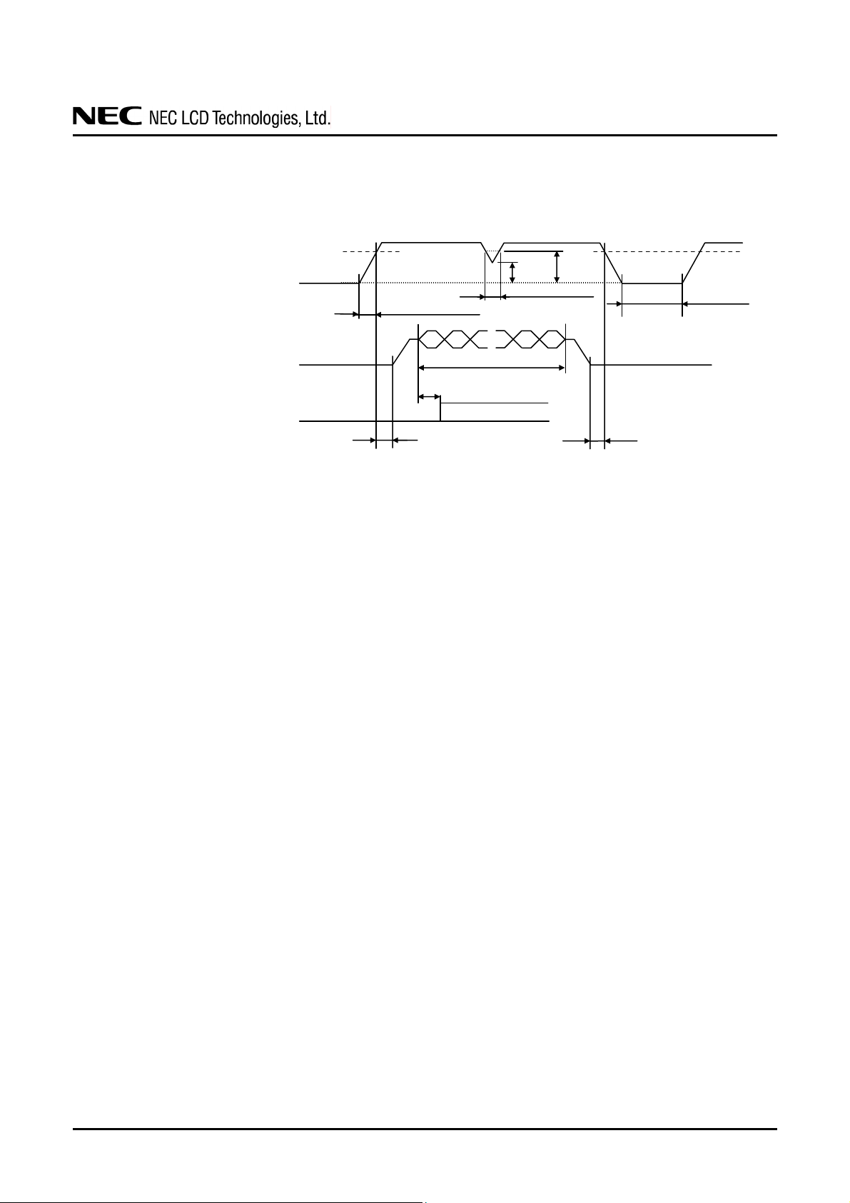
4.4 POWER SUPPLY VOLTAGE SEQUENCE
VDD
Note1, Note2
10.8V
0V
LVDS Signals *1,*2
Note3
0V
CS, SCLK, SDAT
Note3
0V
*1: DA0+/-, DA1+/-, DA2+/-, DA3+/-, CKA+/-, DB0+/-, DB1+/-, DB2+/-, DB3+/-, CKB+/-,
DC0+/-, DC1+/-, DC2+/-, DC3+/-, CKC+/-, DD0+/-, DD1+/-, DD2+/-, DD3+/-, CKD+/-
*2: LVDS signals should be measured at the terminal of 100Ω resistance.
Note1: In terms of voltage variation (voltage drop) while VDD rising edge is below 10.8V, a protection
circuit may work, and then this product may not work.
Note2: VDD should be 10.8V or more during VDD ON period.
Note3: LVDS signals and CS, SCLK, SDAT must be Low or High-impedance, exclude the VALID
period (See above sequence diagram), in order to avoid that internal circuits is damaged.
If some of signals are cut while this product is working, even if the signal input to it once again,
it might not work normally. If customer stops the display and function signals, they should be
cut VDD.
Note4: At the beginning of the serial communication mode, take 20ms or more after the LVDS signal
input. When writing the LUT data, see “4.12 TEN-bit LOOK UP TABLE FOR GAMMA
ADJUSTMENT”.
Note5: The backlight inverter voltage should be inputted within the valid period of LVDS signals, in
order to avoid unstable data display.
VDD ON
5ms < Tr < 80ms
10ms < t < 35ms
VALID period
t≥20ms Note4
VALID period
NL204153BM21-01/-01A
VDD OFF
10.8V
9.6V
VDD dip < 20ms
0ms < t < 35ms
10.8V
Toff > 200ms
DATA SHEET DOD-PD-0556 (2nd edition)
11
 Loading...