

NEC NL128102AC23-02A Datasheet
DATA SHEET
NL128102AC23-02A
TFT COLOR LCD MODULE
39 cm (15.4 inches), 1280
××××
1024 pixels, Full-color,
Multi-scan Function
Incorporated backlight with inverter
DESCRIPTION
NL128102AC23-02A is a TFT (thin film transistor) active matrix color liquid crystal display (LCD) comprising
amorphous silicon TFT attached to each signal electrode, a driving circuit and a backlight. NL128102AC23-02A
has a built-in backlight with an inverter.
The 39 cm (15.4 inches) diagonal display area contains 1280 × 1024 pixels and can display full-color (more than
16 million colors simultaneously). Also, it has multi-scan function.
NL128102AC23-02A is a model which mounted the CRT interface board on NL128102AC23-02.
FEATURES
• Wide viewing angle (with retardation film)
• CRT interface board
• Auto recognition of input signal (Analog RGB signals, Synchronous signals (Hsync, Vsync, Composite))
• Digital control: e.g., Brightness, Display position, contrast, CLK delay
• Free supply voltage sequence
• Corresponding to DDC
• Corresponding to VESA
• On Screen Display
Regarding the use of OSD, please note that there is possibility of conflicts with a patent in Europe and the
U.S. Thus, if such conflict might happen when you use OSD, we shall not be responsible for any trouble.
• Multi-scan function: e.g., SXGA, XGA, SVGA, VGA, VGA-TEXT, MAC
• Incorporated edge type backlight with an inverter (Four lamps into two lamp holders)
• Lamp holder replaceable
VESA : Video Electronics Standards Association
DPMS: Display Power Management Signaling
All trademarks used within this document are the property of their respective owners. VESA, DDC, DPMS and
EDID are trademarks of the Video Electronics Standard Association.
TM
1 and DDC2B
TM
, DPMS
TM
• High luminance (200 cd/m
• Low reflection
DDC1 : Display Data Channel 1
DDC2B: Display Data Channel 2B
2
, TYP.)
APPLICATIONS
• Desk-top type of PC
• Engineering work station
The information in this document is subject to change without notice.
Document No. EN0427EJ1V0DS00 (1st edition)
Date Published February 1999 P
Printed in Japan
1999©
NL128102AC23-02A
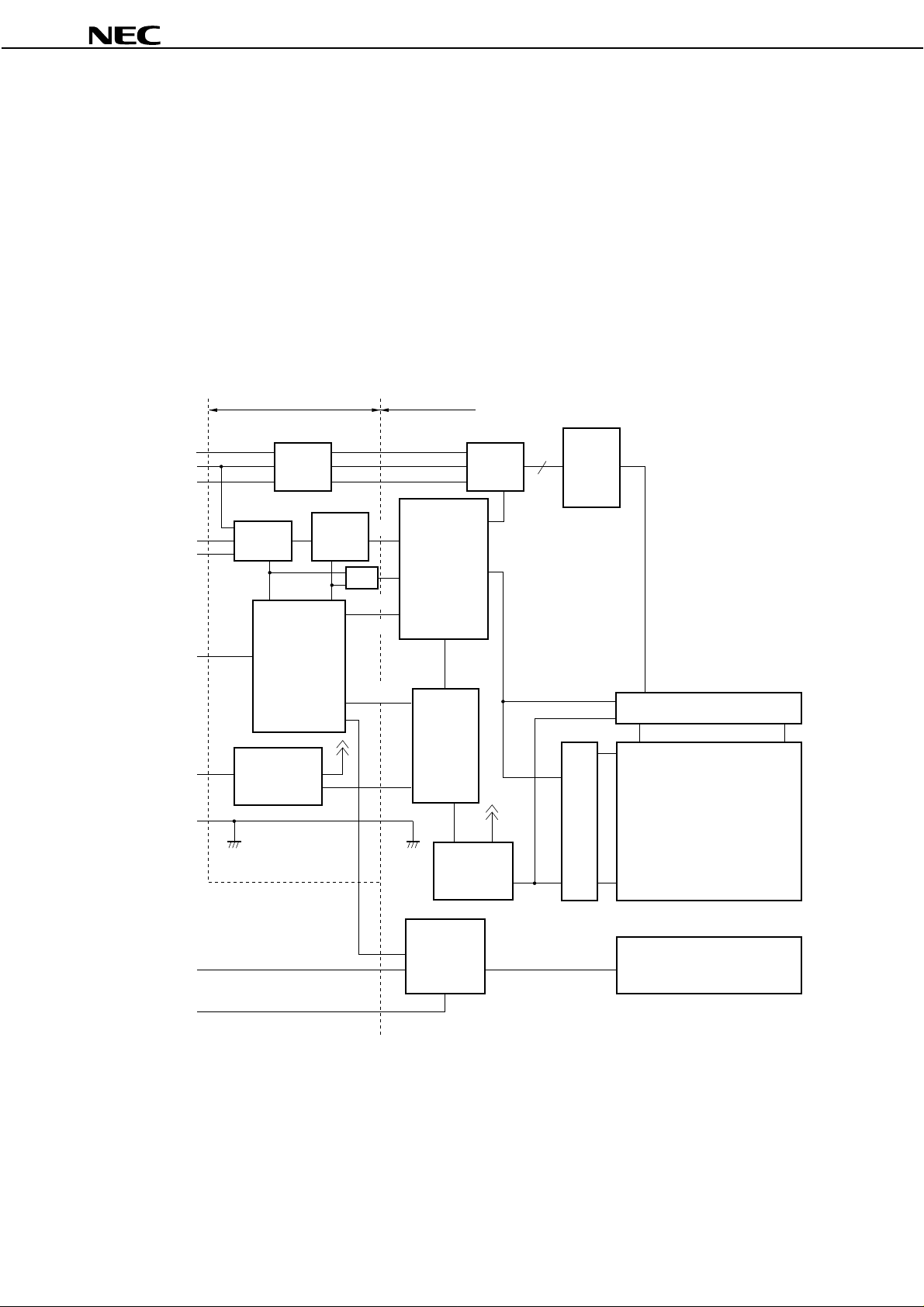
STRUCTURE AND FUNCTIONS
A color TFT (thin film transistor) LCD module is comprised of a TFT liquid crystal panel structure, LSIs for driving
the TFT array, and a backlight assembly. The TFT panel structure is created by sandwiching liquid crystal material
in the narrow gap between a TFT array glass substrate and a color filter glass substrate. After the driver LSIs are
connected to the panel, the backlight assembly is attached to the backside of the panel.
RGB (red, green, blue) data signals from a source system is modulated into a form suitable for active matrix
addressing by the onboard signal processor and sent to the driver LSIs which in turn addresses the individual TFT
cells.
Acting as an electro-optical switch, each TFT cell regulates light transmission from the backlight assembly when
activated by the data source. By regulating the amount of light passing through the array of red, green, and blue
dots, color images are created with clarity.
BLOCK DIAGRAM
Hsync/Csync
Vsync
LEDON
LEDOFF
LED00 to 12
SEL
UP
DOWN
EXIT
VOLSEL
OSDSEL
MENUSEL
DDCCLK
DDCDAT
WPRT
BRTVOL
DD
V
(+12 V)
GND
CLK
OSD
Sync.
Serial
POWER
LCD module
R
G
B
Timing
Controller
ON/OFF
DD
V
AIF
AMP
V-driver
H-driver
3840 lines
LCD panel
1024 lines
I/F Board
R
G
B
Sync.
Division
AMP
PLL
Controller
(Signal
recognition)
DC/DC
converter
2
Luminance
(on/off)
V
DD
B
(+12 V)
GNDB
Neither GND nor GNDB is connected to Frame.
Note
DC/DC
converter
Inverter
Data Sheet EN0427EJ1V0DS00
H: 1280 × 3 (R,G,B)
V: 1024
Backlight

NL128102AC23-02A
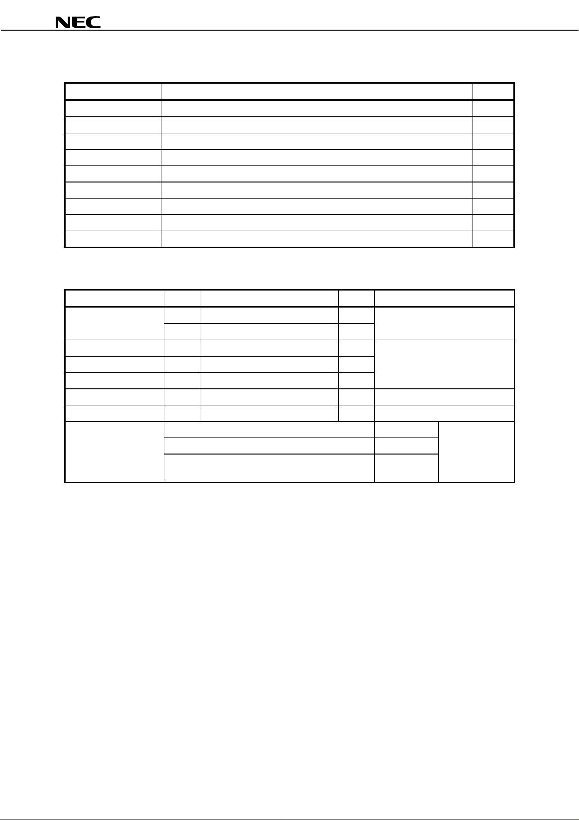
OUTLINE OF CHARACTERISTICS (at room temperature)
Display area 305.28 (H) × 244.224 (V) mm
Drive system a-Si TFT active matrix
Display colors Full-color
Number of pixels 1280 × 1024 pixels
Pixel arrangement RGB vertical stripe
Pixel pitch 0.2385 (H) × 0.2385 (V) mm
Module size 350.0 (H) × 284.8 (V) × 26.0 (max.) (D) mm
Weight 1700 g (TYP.)
Contrast ratio 200 : 1 (TYP.)
Viewing angle (more than the contrast ratio of 10 : 1)
Horizontal : 60° (TYP., left side, right side)
Vertical : 50° (TYP., up side), 45° (TYP., down side)
Color gamut 59% (TYP., at center, to NTSC)
Response time 7 ms (TYP.), white to black
Luminance 200 cd/m
Signal system Analog RGB signals, Synchronous signals (Hsync and Vsync or Composite),
CLK
Supply voltages 12 V (Logic/LCD driving), 12 V (Backlight)
Backlight Edge light type: Four cold cathode fluorescent lamps with an inverter
Power consumption 28.8 W (TYP.)
2
(TYP.)
[Replaceable parts]
• Lamp holder: type No. 154LHS02
• Inverter: type No. 154PW021
Data Sheet EN0427EJ1V0DS00
3
NL128102AC23-02A
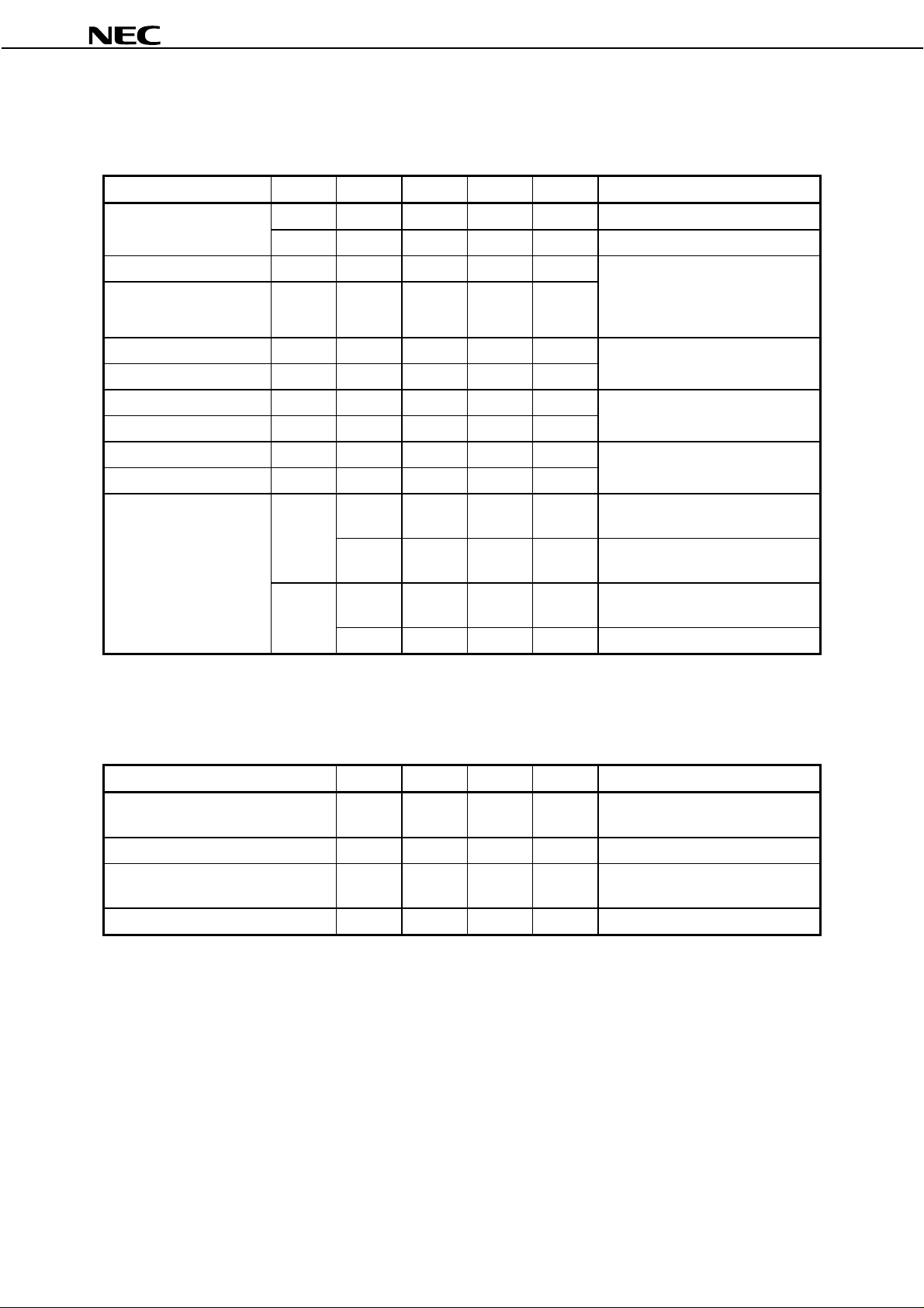
GENERAL SPECIFICATIONS
Item Specification Unit
Module size 350.0 ± 0.6 (H) × 284.8 ± 0.6 (V) × 26.0 (MAX.) (D) mm
Display area 305.28 (H) × 244.224 (V) mm
Number of dots 1280 × 3 (H) × 1024 (V) dot
Number of pixels 1280 (H) × 1024 (V) pixel
Dot pitch 0.0795 (H) × 0.2385 (V) mm
Pixel pitch 0.2385 (H) × 0.2385 (V) mm
Pixel arrangement RGB (Red, Green, Blue) vertical stripe –
Display colors full color color
Weight 1760 (MAX.) g
ABSOLUTE MAXIMUM RATINGS
Parameter Symbol Rating Unit Remarks
V
Logic input voltage V
R,G,B input voltage V
CLK input voltage V
Storage temp. T
Operating temp. T
Humidity
≤
≤
Absolute humidity shall not exceed T
relative humidity level.
Measured at the LCD panel
Note
DD
V
DD
B –0.3 to +14 V
IN1
IN2
IN3
ST
OP
–0.3 to +14 VSupply voltage
–0.3 to +5.5 V
–6.0 to +6.0 V
–7.0 to +7.0 V
–20 to + 60 °C –
0 to +50 °C
95% relative humidity T
85% relative humidity
a
= 50°C, 85%
a
T
= 25°C
a
= 25°C
T
DD
= 12 V
V
Module surface
a
≤ 40°C
40 < Ta ≤ 50°C
Ta > 50°C
Note
No condensation
4
Data Sheet EN0427EJ1V0DS00
ELECTRICAL CHARACTERISTICS
(1) Logic, LCD driving, Backlight
Parameter Symbol MIN. TYP. MAX. Unit Remarks
VDDB 11.4 12.0 12.6 V for backlightSupply voltage
DD
V
Logic input Low voltage V
Logic input High voltage V
Logic output Low voltage V
Logic output High voltage V
Logic input Low current 1 I
Logic input High current 1 I
Logic input Low current 2 I
Logic input High current 2 I
Supply current
IL
IH
OL
OH
iL1
iH1
iL2
iH2
DD
I
DD
I
B
NL128102AC23-02A
T
11.4 12.0 12.6 V for logic and LCD driving
0–0.8V
2.0 – 5.25 V
––0.4V
2.4 – – V
–1 – –
––1
––1
–1 – –
µ
µ
µ
µ
– 1000 1500 mA for LCD driving
– 50 65 mA Power saving mode, VDD = 12.0 V
– 1400 1600 mA for back light
– 1 10 mA Power saving mode, V
Hsync/Csyn c, Vsync, SEL, UP,
DOWN, EXIT, VOLSEL, DDCDAT ,
DDCCLK, OSDSEL, WPRT,
MENUSEL
DDCDAT
Hsync/Csync, Vsync
A
A
DDCDAT
A
A
DD
= 12.0 V
V
DD
B = 12.0 V
V
DD
B = 12.0 V
a
= 25°C
Note
Note
Pixel checkered pattern
Note
(2) Video signal (R,G,B) input
Item MIN. TYP. MAX. Unit Remarks
Maximum amplitude (white - black) 0
(black)
DC input level (black) –0. 5 – +2.5 V –
Sync. level 0.2 0.3 *B Vp-p G terminal
*A + *B – – 1.1 Vp-p –
0.7
(white)
*A Vp-p Need to adjust contrast if input more
0.7 Vp-p
(Sync. On Green)
a
= 25°C
T
Data Sheet EN0427EJ1V0DS00
5
NL128102AC23-02A
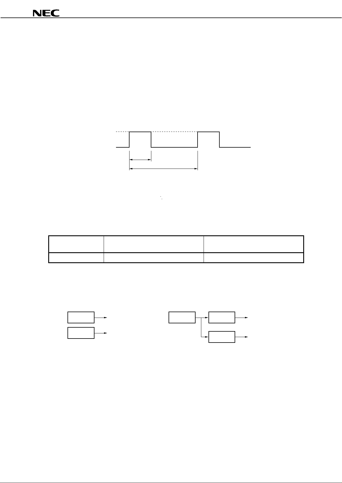
POWER SUPPLY DESIGN
(1) Please note that the supply voltage must not be applied while the control signals (SEL, UP, DOWN, EXIT,
BRT+ and BRT–) are connected to GND. Otherwise the module may cause malfunction.
(2) If the power supply voltage is applied while UP and DOWN are connected to GND, the input control signals
become ineffective. In this case, please turn off the power once and turn on the power while UP and DOWN are
connected to GND again.
(3) Inverter current wave
Inverter current wave is as follows.
1400 (mA)
0 (A)
Duty
Luminance control frequency
Maximum luminance control: 100%
Minimum luminance control: 20%
Luminance control frequency Input Vsync frequency × K
(4) Ripple of supply voltage
Acceptable range
Remark
The acceptable range of ripple voltage includes spike noise.
Example of the power supply connection
a) Separate the power supply b) Put the filter
Power VDD
Power VDDB
=
Input Vsync frequency ≤ 75 Hz: K = 4.6
Input Vsync frequency > 75 Hz: K = 3.6
DD
V
(for logic and LCD driver)
≤
100 mVp-p
Power
DD
V
B
(for backlight)
≤
200 mVp-p
Filter* VDD
Filter* VDDB
6
Data Sheet EN0427EJ1V0DS00
NL128102AC23-02A
INTERFACE PIN CONNECTION
(1) Interface signals, power supply
CN101
Part No. : MRF03-6R-SMT
Adaptable socket : MRF03-6P-1.27 (For cable type) or MRF03-6PR-SMT (For board to board type)
Supplier : HIROSE ELECTRIC CO., LTD.
Pin No. Symbol Pin No. Sym bol
1B 4 Vsync
2 G 5 Hsync/Csync
N.C.
3R 6
N.C. (No connection) should be open.
Note
Note
CN102
Part No. : IL-Z-4PL-SMTY
Adaptable socket : IL-Z-4S-S125C3
Supplier : Japan Aviation Electronics Industry Limited (JAE)
Pin No. Symbol Pin No. Sym bol
1 DDCCLK 3 MENUSEL
2 DDCDAT 4 GND
CN103
Part No. : DF14A-25P-1.25H
Adaptable socket : DF14-25S-1.25C
Supplier : HIROSE ELECTRIC CO., LTD. (coaxial type)
Figure from socket view
······12 56
Figure from socket view
4321
Pin No. S ymbol Pin No. Symbol
1 LEDON 14 EXIT
2LEDOFF15 GND
3GND16BRTVOL
4 LED00 17 GND
5 LED01 18 VOLSEL
6 LED02 19 OSDSEL
7 LED10 20 WPRT
8 LED11 21 TEST1
9 LED12 22 TEST2
10 GND 23 GND
11 SEL 24 TEST3
12 UP 25 TEST4
13 DOWN
TEST1 to 4 should be open.
Note
Figure from socket view
····
1 2 24 25
Data Sheet EN0427EJ1V0DS00
7
CN104
Part No. : IL-Z-8PL-SMTY
Adaptable socket : IL-Z-8S-S125C3
Supplier : Japan Aviation Electronics Industry Limited (JAE)
NL128102AC23-02A
Pin No. S ymbol Pin No. Symbol
1VDD5GND
2VDD6GND
3VDD7GND
4VDD8GND
CN201
Part No. : IL-Z-11PL1-SMTY
Adaptable socket : IL-Z-11S-S125C3
Supplier : Japan Aviation Electronics Industry Limited (JAE)
Pin No. S ymbol Pin No. Symbol
1V
2V
3V
4 GNDB 10 N.C.
5 GNDB 11 N.C.
6 GNDB
DD
B 7 N.C.
DD
B 8 N.C.
DD
B 9 N.C.
Figure from socket view
87 21·····
Figure from socket view
11 10 2 1·····
N.C. (No connection) should be open.
Note
<Connector location>
Rear view
11
1
CN101
6
3
CN102
CN201
1
1
1
CN103
25
8
CN104
1
8
Data Sheet EN0427EJ1V0DS00
(2) Pin function
Symbol I/O Logic Description
NL128102AC23-02A
Hsync/
Csync
Vsync Input Negative Vertic al sync hronous si gnal i nput (TTL level)
R Input – Red video signal input (0.7 Vp-p, 75 Ω)
G Input – Green video signal input (0.7 Vp-p, 75 Ω)
B Input – Blue video signal input (0.7 Vp-p, 75 Ω)
SEL Input Negative Control function sel ect signal (TTL level)
UP Input Negative Control signal (TTL level)
DOWN Input Negative Control signal (TTL level)
EXIT Input Negative Control signal (TTL level)
OSDSEL Input –
MENUSEL Input – OSD design select signal
BRTVOL Input – Volume luminance control
VOLSEL Input – Luminance control select signal
DDCCLK Input P ositive CLK for DDC2B
DDCDAT Input/
LEDON Output Positive Indicator for LED power on
LEDOFF Output Positive Indicator for power save mode
Input Negative Horizontal synchronous signal input or composite synchronous signal input
(TTL level) , Positive/Negative auto recognition
Positive/Negative auto recognition, Cl ock i nput f o r DDC1
SEL is pulled up in the module.
Output
Detail of the functions are mentioned in
High or open: SEL off, Low: SEL on
The signal increases the value of the functions selected.
UP is pulled up in tha module.
High or open: UP off, Low: UP on
The signal decreases the value of the functions selected.
DOWN is pulled up in the module.
High or open: DOWN off, Low : Down on
The signal initializes the selected function.
EXIT is pulled up in the module.
High or open: EXIT off, Low: EXIT on
Display select signal
OSDSEL is pulled up in the module.
“H or open”: OSD display off (light on LED)
“L”: OSD display on (light off LED)
Details of the functions are mentioned in
MENUSEL is pulled up in the module.
“H or open”: OSD display No.2
“L”: OSD display No.1(Transparent background)
Detail of the functions are mentioned in
Detail of the functions are mentioned in
SELECTION
VOLSEL is pulled up in the module.
Details of the functions are mentioned in
SELECTION
Positive Data for DDC1/2B
read/write
“H”: LED select, “L”: Other status
“H”: power save mode select, “L”: Other status
CONTROL FUNCTIONS
CONTROL FUNCTIONS
OSD DESIGN SELECT
LUMINANCE CONTROL
LUMINANCE CONTROL
.
Data Sheet EN0427EJ1V0DS00
9
Symbol I/O Logic Description
NL128102AC23-02A
LED00 Output Positive
LED01 Output Positive
LED02 Output Positive
LED10 Output Negative
LED11 Output Negative
LED12 Output Negative
WPRT I nput Positive Select signal for DDC
TEST1 to 4 Output Positiv e Reserve. TEST 1 to 4 should be open.
DD
V
VDDB – – Power supply for backlight. +12 V (±5 %)
GND – – Ground for system. Signal ground for logic/LCD driving
GNDB – – Ground for backlight. GNDB is not connected to the module GND (FG).
Remark
– – Power supply for Logic and LCD driving +12 V (±5 %)
Frame ground, system ground and backlight ground are not connected into the module.
See detail of
FUNCTIONS
“open”: Reading mode, “L”: Writing mode
EQUIVALENT CIRCUIT FOR LEDS and CONTROL
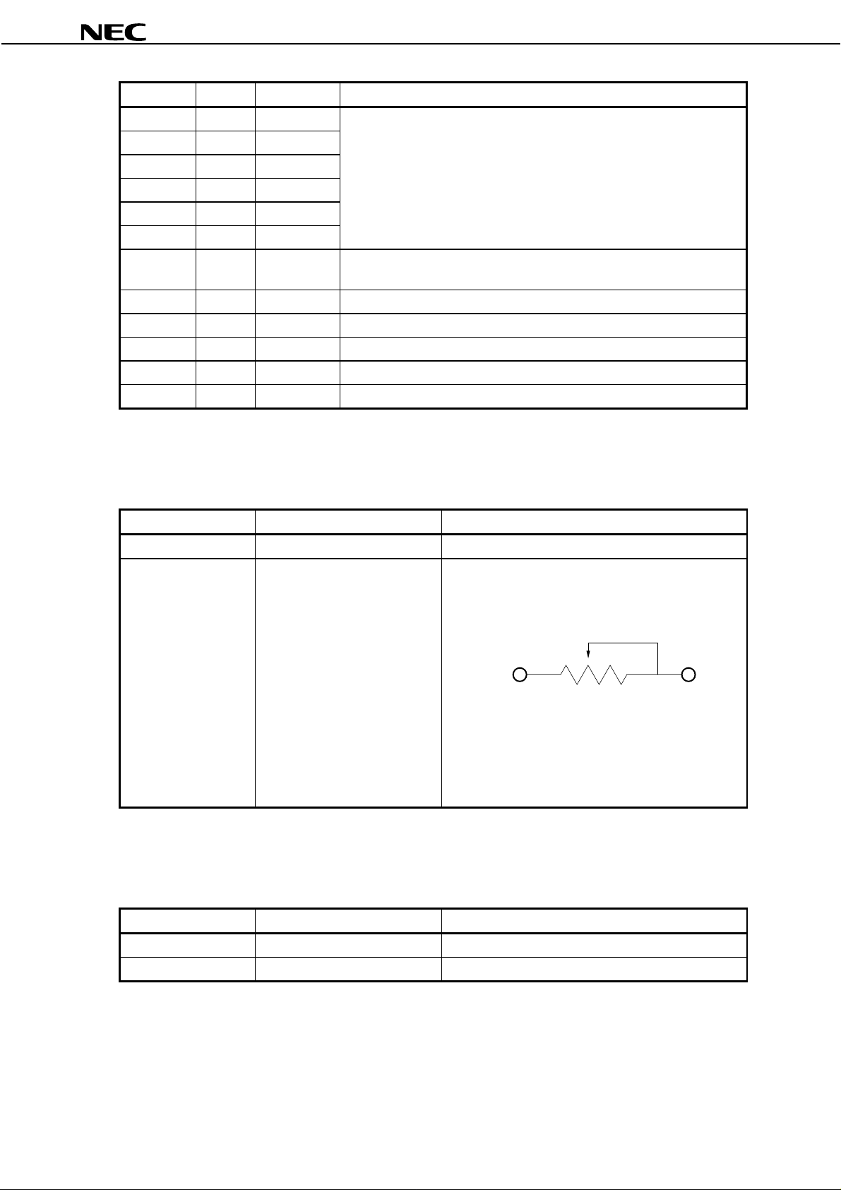
(3) LUMINANCE CONTROL SELECTION
VOLSEL= “L” “Open”
Form Digital adjust Volume adjust
See
How to adjust
The status of VOLSEL is valid when the power is switched on.
Note
CONTROL FUNCTIONS
(4) FUNCTION DISPLAY SELECT
OSDSEL= “L” “Open”
Form OSD Display LED Dispaly
See
How to adjust
CONTROL FUNCTIONS
The variable resistor for luminance control should be 10
kΩ type, and zero point of the resistor corresponds to the
minimum of luminance.
BRTVOL GND
R
Maximum luminance (100%): R = 10 K
Minimum luminance (30%): R = 0
Mating variable resistor: 10 KΩ ±5%,
B curve, 1/10 W
See Example of LED circuit. (Next page)
Ω
Ω
The status of OSDSEL is valid when the power is switched on.
Note
OSD
Regarding the use of OSD, please note that there is possibility of conf licts w ith a patent in Europ e and the U .S.
Thus, if such conflict might happen when you use OSD, we shall not be responsible for any trouble.
10
Data Sheet EN0427EJ1V0DS00
(5) OSD DESIGN SELECT
MENUSEL= “L” “Open”
Form OSD display No. 1 OSD display No. 2
How to adjust
The status of MENUSEL is valid when the power is switched on.
Note
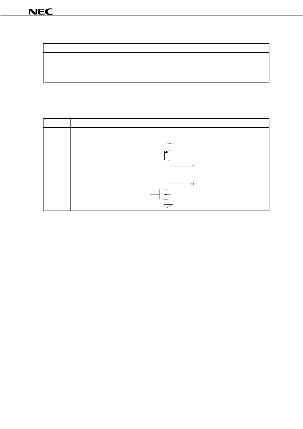
(6) Equivalent circuit
Symbol I/O Equivalent circuit
See
CONTROL FUNCTIONS
(OSD background is
transparent)
See
CONTROL FUNCTIONS
NL128102AC23-02A
LEDON
LEDOFF
LED00
LED01
LED02
LED10
LED11
LED12
Output RN2306 (Tos hi ba)
or equivalent
Output
Output N-c h Open Drai n Output
Output
Data Sheet EN0427EJ1V0DS00
11
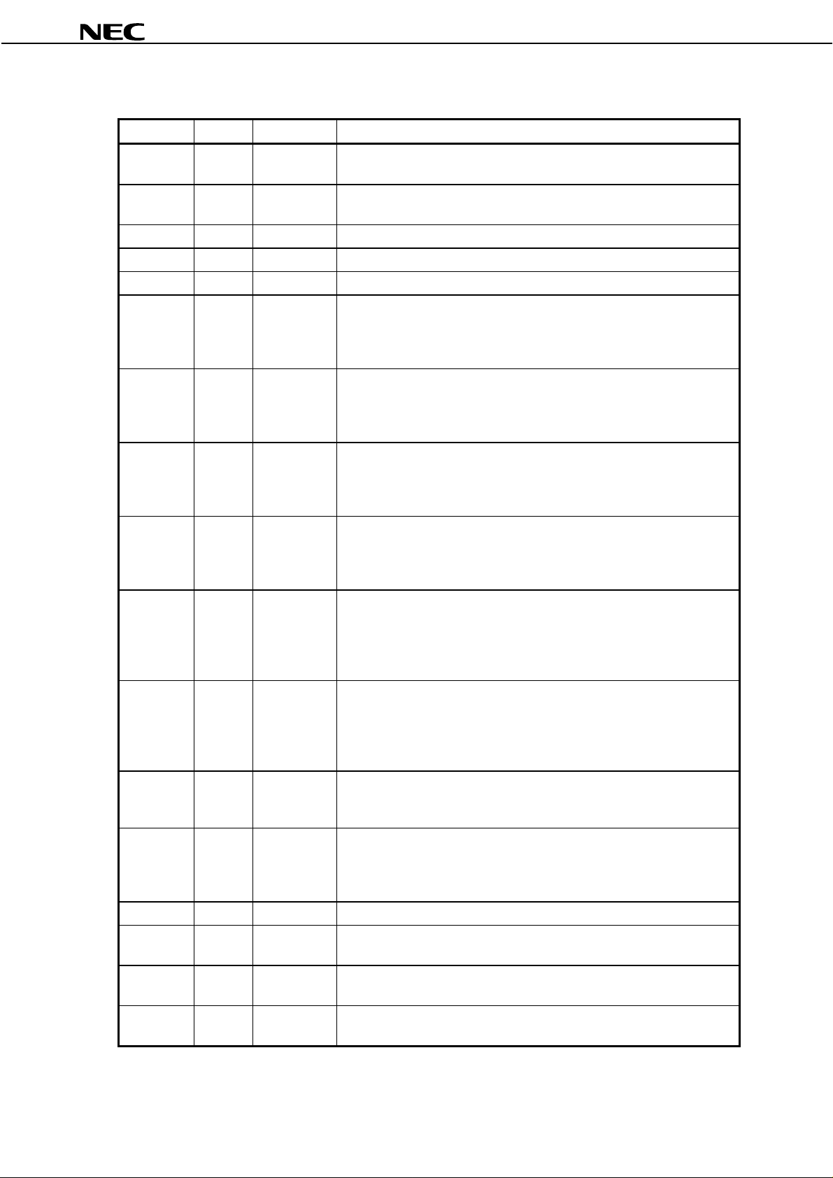
<Recommendation circuit diagram>
Input LCD module Output
SEL
CN103
NL128102AC23-02A
Two color LED
R (330 Ω)
LEDON
LEDOFF
R (330 Ω)
UP
DOWN
EXIT
VOLSEL
OSDSEL
LED1
LED00
R (330 Ω)
LED2
LED3
LED4
LED01
R (330 Ω)
LED5
LED6
LED7
LED02
R (330 Ω)
LED8
LED9
<LED status>
LED1: Brightness
LED2: Contrast
LED3: Horizontal display period
LED4: CLK delay
LED5: Vertical position
LED6: Horizontal position
LED7: Reserve
LED8: All reset
LED9: Reserve
LED10
LED11
LED12
12
Data Sheet EN0427EJ1V0DS00
 Loading...