

Page 1

TFT COLOR LCD MODULE
NL10276BC30-32D
38cm (15.0 Type)
XGA
LVDS interface (1port)
DATA SHEET
DOD-PP-1223 (5th edition)
This DATA SHEET is updated document from
DATA SHEET DOD-PP-1052 (4).
All information is subject to change without notice.
Please confirm the sales representative before
starting to design your system.
Document Number: DOD-PP-1223 (5th edition)
Published date: May 2011 CP(N)
1
© NEC LCD Technologies, Ltd.
2007-2011 All rights reserved.
Page 2

NL10276BC30-32D
INTRODUCTION
The Copyright to this document belongs to NEC LCD Technologies, Ltd. (hereinafter called "NEC").
No part of this document will be used, reproduced or copied without prior written consent of NEC.
NEC does and will not assume any liability for infringement of patents, copyrights or other intellectual
property rights of any third party arising out of or in connection with application of the products
described herein except for that directly attributable to mechanisms and workmanship thereof. No license,
express or implied, is granted under any patent, copyright or other intellectual property right of NEC.
Some electronic parts/components would fail or malfunction at a certain rate. In spite of every effort to
enhance reliability of products by NEC, the possibility of failures and malfunction might not be avoided
entirely. To prevent the risks of damage to death, human bodily injury or other property arising out
thereof or in connection therewith, each customer is required to take sufficient measures in its safety
designs and plans including, but not limited to, redundant system, fire-containment and anti-failure.
The products are classified into three quality grades: "Standard", "Special", and "Specific" of the
highest grade of a quality assurance program at the choice of a customer. Each quality grade is designed
for applications described below. Any customer who intends to use a product for application other than
that of Standard quality grade is required to contact an NEC sales representative in advance.
The Standard quality grade applies to the products developed, designed and manufactured in
accordance with the NEC standard quality assurance program, which are designed for such application as
any failure or malfunction of the products (sets) or parts/components incorporated therein a customer
uses are, directly or indirectly, free of any damage to death, human bodily injury or other property, like
general electronic devices.
Examples: Computers, office automation equipment, communications equipment, test and measurement
equipment, audio and visual equipment, home electronic appliances, machine tools, personal
electronic equipment, industrial robots, etc.
The Special quality grade applies to the products developed, designed and manufactured in accordance
with an NEC quality assurance program stricter than the standard one, which are designed for such
application as any failure or malfunction of the products (sets) or parts/components incorporated therein
a customer uses might directly cause any damage to death, human bodily injury or other property, or
such application under more severe condition than that defined in the Standard quality grade without
such direct damage.
Examples: Control systems for transportation equipment (automobiles, trains, ships, etc.), traffic control
systems, anti-disaster systems, anti-crime systems, medical equipment not specifically
designed for life support, safety equipment, etc.
The Specific quality grade applies to the products developed, designed and manufactured in accordance
with the standards or quality assurance program designated by a customer who requires an extremely
higher level of reliability and quality for such products.
Examples: Military systems, aircraft control equipment, aerospace equipment, nuclear reactor control
systems, medical equipment/devices/systems for life support, etc.
The quality grade of this product is the "Standard" unless otherwise specified in this document.
DATA SHEET DOD-PP-1223 (5th edition)
2
Page 3

NL10276BC30-32D
CONTENTS
INTRODUCTION ............................................................................................................................................2
1. OUTLINE......................................................................................................................................................4
1.1 STRUCTURE AND PRINCIPLE.............................................................................................................4
1.2 APPLICA TION.........................................................................................................................................4
1.3 FEATURES...............................................................................................................................................4
2. GENERAL SPECIFICATIONS ..................................................................................................................5
3. BLOCK DIAGRAM.....................................................................................................................................6
4. DETAILED SPECIFICATIONS.................................................................................................................7
4.1 MECHANICAL SPECIFICATIONS........................................................................................................7
4.2 ABSOLUTE MAXIMUM RATINGS ......................................................................................................7
4.3 ELECTRICAL CHARACTERISTICS.....................................................................................................8
4.3.1 LCD panel signal processing board ...................................................................................................8
4.3.2 Backlight lamp...................................................................................................................................9
4.3.3 Power supply voltage ripple.............................................................................................................10
4.3.4 Fuse..................................................................................................................................................10
4.4 POWER SUPPLY VOLTAGE SEQUENCE..........................................................................................11
4.5 CONNECTIONS AND FUNCTIONS FOR INTERFACE PINS...........................................................12
4.5.1 LCD panel signal processing board .................................................................................................12
4.5.2 Backlight lamp.................................................................................................................................13
4.5.3 Positions of plug and socket............................................................................................................13
4.5.4 Connection between receiver and transmitter for LVDS.................................................................14
4.6 DISPLAY COLORS AND INPUT DATA SIGNALS ............................................................................16
4.7 DISPLAY POSITIONS...........................................................................................................................17
4.8 SCANNING DIRECTIONS...................................................................................................................17
4.9 INPUT SIGNAL TIMINGS....................................................................................................................18
4.9.1 Outline of input signal timings ........................................................................................................18
4.9.2 Timing characteristics......................................................................................................................19
4.9.3 Input signal timing chart ..................................................................................................................20
4.10 OPTICS.................................................................................................................................................21
4.10.1 Optical characte ristics....................................................................................................................21
4.10.2 Definition of contrast ratio.............................................................................................................22
4.10.3 Definition of luminance uniformity...............................................................................................22
4.10.4 Definition of response times..........................................................................................................22
4.10.5 Definition of viewing angles..........................................................................................................22
5. ESTIMATED LUMINANCE LIFETIME................................................................................................23
6. RELIABILITY TESTS...............................................................................................................................24
7. PRECAUTIONS .........................................................................................................................................25
7.1 MEANING OF CAUTION SIGNS........................................................................................................25
7.2 CAUTIONS............................................................................................................................................25
7.3 A TTENTIONS........................................................................................................................................25
7.3.1 Handling of the product...................................................................................................................25
7.3.2 Environment.....................................................................................................................................26
7.3.3 Characteristics..................................................................................................................................26
7.3.4 Other................................................................................................................................................27
8. OUTLINE DRAWINGS.............................................................................................................................28
8.1 FRONT VIEW........................................................................................................................................28
8.2 REAR VIEW ............................................................................................................................... ...........29
DATA SHEET DOD-PP-1223 (5th edition)
3
Page 4

1. OUTLINE
1.1 STRUCTURE AND PRINCIPLE
Color LCD module NL10276BC30-32D is composed of the amorphous silicon thin film transistor
liquid crystal display (a-Si TFT LCD) panel structure with driver LSIs for driving the TFT (Thin Film
Transistor) array and a backlight.
The a-Si TFT LCD panel structure is injected liquid crystal material into a narrow gap between the
TFT array glass substrate and a color-filter glass substrate.
Color (Red, Green, Blue) data signals from a host system (e.g. signal generator, etc.) are modulated
into best form for active matrix system by a signal processing board, and sent to the driver LSIs which
drive the individual TFT arrays.
The TFT array as an electro-optical switch regulates the amount of transmitted light from the
backlight assembly, when it is controlled by data signals. Color images are created by regulating the
amount of transmitted light through the TFT array of red, green and blue dots.
1.2 APPLICA TION
• For industrial use
1.3 FEATURES
• Wide viewing angle
• Fast response time
• LVDS interface (8-bit)
• Selectable LVDS input map
• Reversible-scan direction
• Small foot print
• Edge light type backlight (without inverter)
• Replaceable lamp for backlight
• Acquisition product for UL60950-1/CSA C22.2 No.60950-1-03 (File number: E170632)
• Compliant with the European RoHS directive (2002/95/EC)
NL10276BC30-32D
DATA SHEET DOD-PP-1223 (5th edition)
4
Page 5
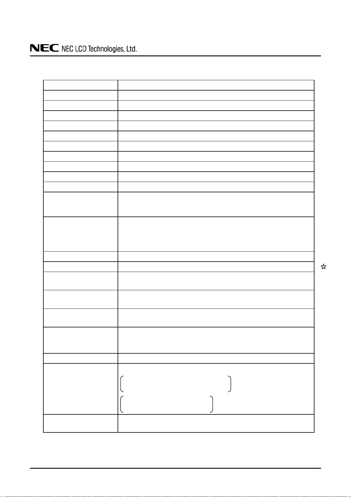
2. GENERAL SPECIFICATIONS
Display area
Diagonal size of display
NL10276BC30-32D
304.128 (H) × 228.096 (V) mm
38cm (15.0 inches)
Drive system
Display color
Pixel
Pixel arrangement
Dot pitch
Pixel pitch
Module size
Weight
Contrast ratio
Viewing angle
Designed viewing direction
Polarizer surface
Polarizer pencil-hardness
a-Si TFT active matrix
16,777,216 colors (6bit+FRC)
1,024 (H) × 768 (V) pixels
RGB (Red dot, Green dot, Blue dot) vertical stripe
0.099 (H) × 0.297 (V) mm
0.297 (H) × 0.297 (V) mm
326.5 (typ., W) × 253.5 (typ., H) × 12.0 (max., D) mm
970g (typ.)
500:1 (typ.)
≥
At the contrast ratio
• Horizontal: Right side 80° (typ.), Left side 80° (typ.)
• Vertical: Up side 80° (typ.), Down side 80° (typ.)
At DPS terminal= Low or Open: Normal scan
• Viewing direction without image reversal: Up side (12 o'clock)
• Viewing direction with contrast peak: Down side (6 o'clock)
• Viewing angle with optimum grayscale (γ≒2.2): Normal axis (perpendicular)
Antiglare
3H (min.) [by JIS K5600]
10:1
Note1
Color gamut
Response time
Luminance
Signal system
Power supply voltage
Backlight
Power consumption
At LCD panel center
50% (typ.) [against NTSC color space]
Ton+Toff (10%
18ms (typ.)
At IBL= 7.5mArms / lamp
250cd/m
LVDS 1port (Receiver: Equivalent of THC63LVDF84B, THine Electronics Inc.)
[8-bit digital signals for data of RGB colors, Dot clock (CLK),
Data enable (DE)]
LCD panel signal processing board: 3.3V
Edge light type: 2 cold cathode fluorescent lamps (without inverter)
Replaceable part
Recommended inverter (Option)
At IBL= 7.5mArms / lamp, Checkered flag pattern
10.0W (typ., Power dissipation of the inverter is not included.)
2
(typ.)
• Lamp holder set: Type No. 150LHS34
• Inverter: Type No. 150PW331
Note1: Excluding lamp cables and projection.
←→
90%)
DATA SHEET DOD-PP-1223 (5th edition)
5
Page 6
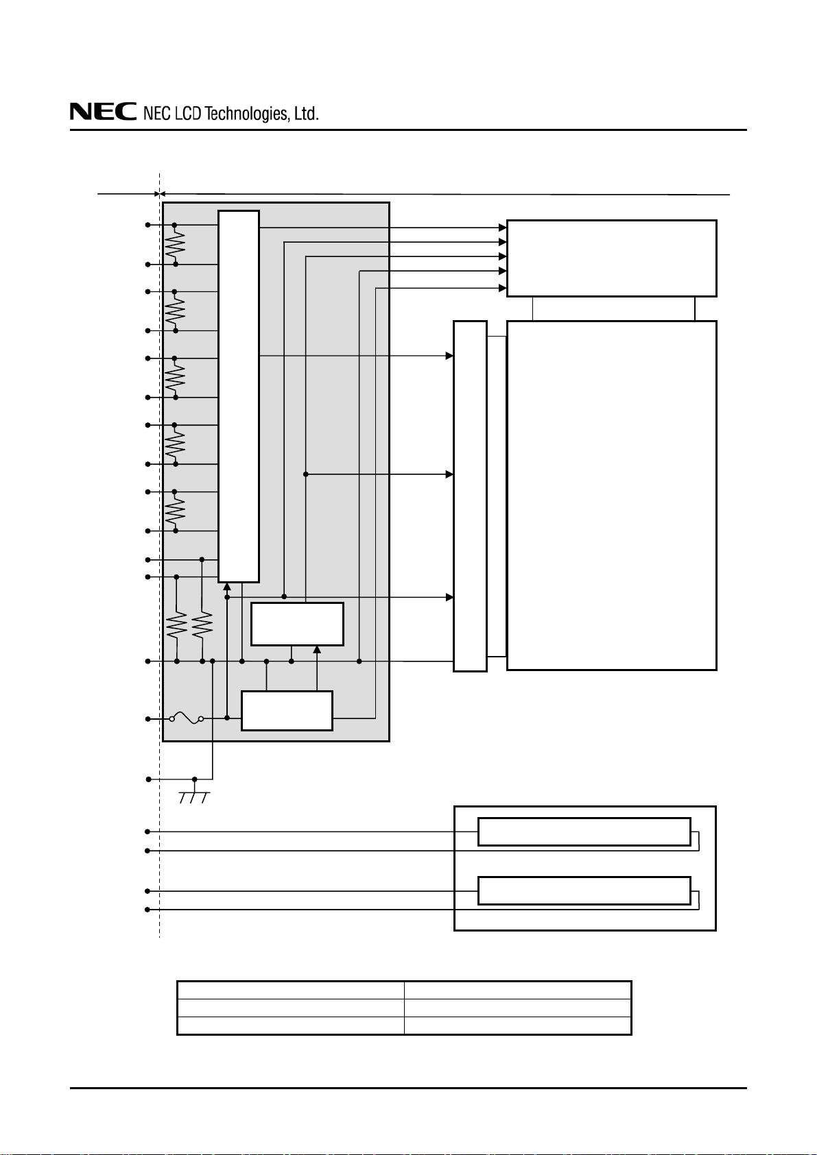
3. BLOCK DIAGRAM
Host
LCD module (Product)
D0+
D0-
100Ω
D1+
D1-
100Ω
D2+
D2-
100Ω
D3+
D3-
100Ω
CLK+
CLK-
100Ω
MSL
DPS
GND
Note1
Note2
VCC
Fuse
FG
Note1
Note2
VBLH
VBLC
Note1
VBLH
VBLC
Note1
Note1: Relations between GND (Signal ground), FG (Frame ground) and VBLC (Lamp low voltage
terminal) in the product are as follows.
GND-FG Connected
GND-VBLC Not connected
FG-VBLC Not connected
Note2: GND and FG must be connected to customer equipment's ground, and it is recommended that
GND, FG and customer inverter ground are connected together in customer equipment.
50kΩ
Controller with receiver for LVDS
50kΩ
Power supply
for gradation
DC/DC
converter
LCD panel signal processing board
NL10276BC30-32D
H-driver
3,072 lines
LCD panel
H: 1,024 × 3 (R, G, B)
V: 768
768 lines
V-driver
Backlight (Edge light type)
1 lamp
1 lamp
DATA SHEET DOD-PP-1223 (5th edition)
6
Page 7
4. DETAILED SPECIFICATIONS
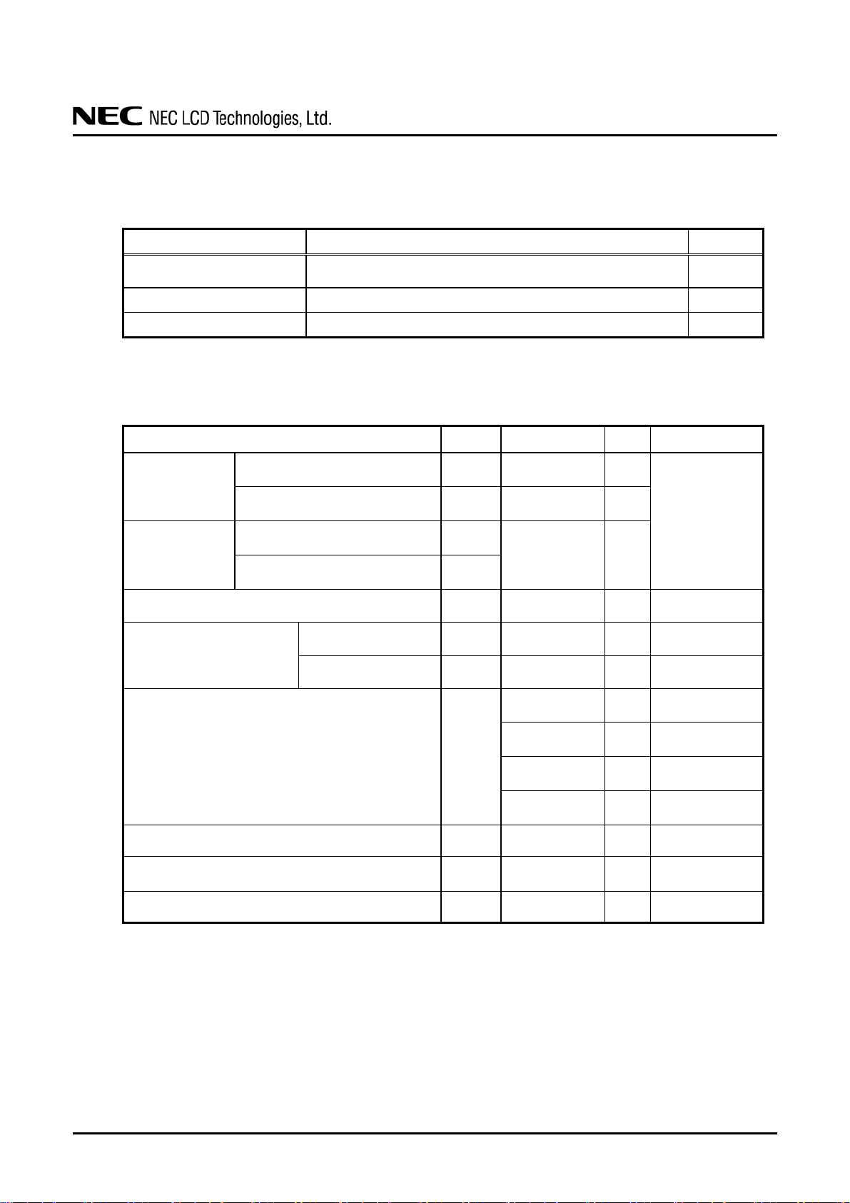
4.1 MECHANICAL SPECIFICATIONS
Parameter Specification Unit
Module size 326.5 ± 0.5 (W) × 253.5 ± 0.5 (H) × 12.0 max. (D)
Display area 304.128 (H) × 228.096 (V) Note2 mm
Weight 970 (typ.), 1,050 (max.) g
Note1: Excluding lamp cables and projection.
Note2: See "8. OUTLINE DRAWINGS".
4.2 ABSOLUTE MAXIMUM RATINGS
Parameter Symbol Rating Unit Remarks
NL10276BC30-32D
Note1,
Note2
mm
Power supply
voltage
Input voltage for
signals
Operating temperature
LCD panel signal processing board VCC -0.3 to +3.6 V
Lamp voltage VBLH 2,000 Vrms
Display signals
Note1
Function signals
Note2
Storage temperature Tst -20 to +80
Front surface TopF -20 to +70
Rear surface TopR -20 to +70
Relative humidity
Note5
Absolute humidity
Note5
Operating altitude -
VD
VF
RH
AH
-0.3 to +3.6
and
<VCC +0.3
≤ 95
≤ 85
≤ 55
≤ 36
≤ 70
Note6
≤ 4,850
V
°C
°C
°C
%
%
%
%
g/m
m
Note3
Note4
Ta ≤ 40°C
40 < Ta ≤ 50°C
50 < Ta ≤ 60°C
60 < Ta ≤ 70°C
3
Ta > 70°C
-20°C ≤ Ta ≤ 70°C
-
-
Storage altitude -
≤ 13,600
m
-20°C ≤ Ta ≤ 80°C
Note1: D0+/-, D1+/-, D2+/-, D3+/-, CLK+/Note2: MSL, DPS
Note3: Measured at center of LCD panel surface (including self-heat)
Note4: Measured at center of LCD module's rear shield surface (including self-heat)
Note5: No condensation
Note6: Water amount at Ta= 70°C and RH= 36%
DATA SHEET DOD-PP-1223 (5th edition)
7
Page 8
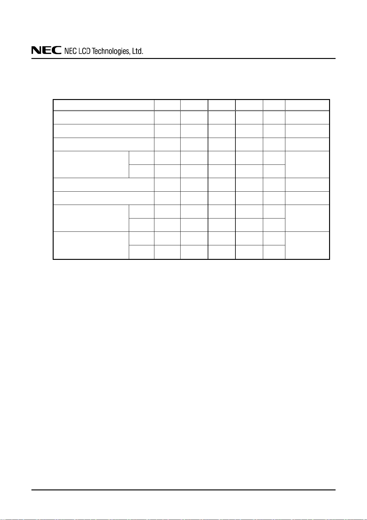
4.3 ELECTRICAL CHARACTERISTICS
4.3.1 LCD panel signal processing board
Parameter Symbol min. typ. max. Unit Remarks
Power supply voltage VCC 3.0 3.3 3.6 V -
Power supply current ICC -
Permissible ripple voltage VRP - - 100 mVp-p for VCC
500
Note1
NL10276BC30-32D
(Ta= 25°C)
700
Note2
mA at VCC= 3.3V
Differential input threshold
voltage for LVDS receiver
Input voltage swing for LVDS receiver Vi 0 - 2.4 V -
Terminating resistance RT - 100 -
Input voltage for
MSL and DPS signals
Input current for
MSL and DPS signals
High VTH - - +100 mV
Low VTL -100 - - mV
Ω
High VFH 2.0 - VCC V
Low VFL 0 - 0.8 V
High IFH - - 300
Low IFL -300 - -
μA
μA
at VCM= 1.2V
Note3
-
-
-
Note1: Checkered flag pattern [by EIAJ ED-2522]
Note2: Pattern for maximum current
Note3: Common mode voltage for LVDS receiver
DATA SHEET DOD-PP-1223 (5th edition)
8
Page 9
⏐
⏐
×
⏐
×
4.3.2 Backlight lamp
Lamp current
Lamp voltage
Lamp starting voltage
Lamp oscillation frequency
Note1: This product consists of 2 backlight lamps, and these specifications are for each lamp.
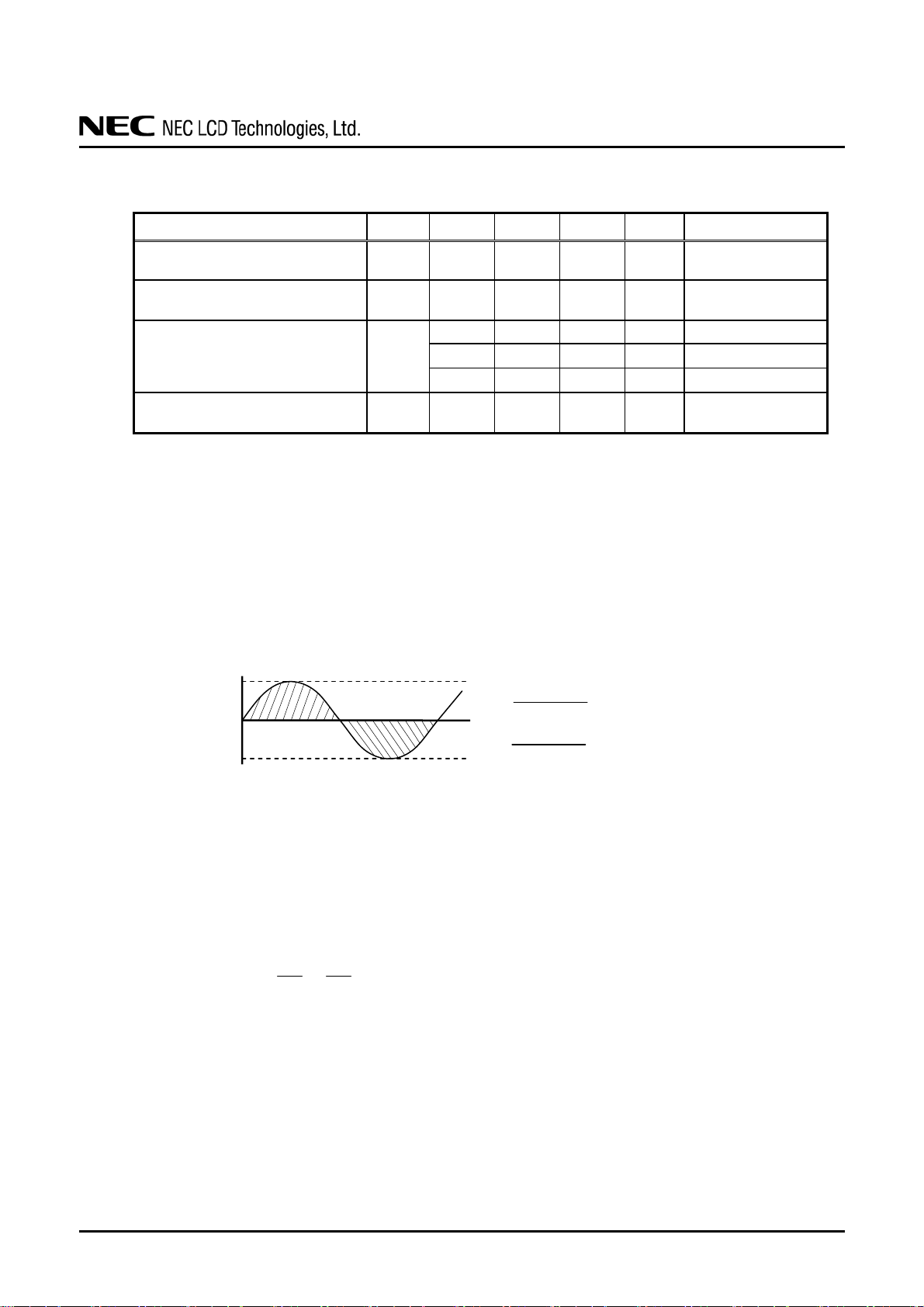
Note2: The lamp voltage cycle between lamps should be kept on a same phase. "VS" and "VBLH"
Note3: The asymmetric ratio of working waveform for lamps (Lamp voltage peak ratio, Lamp current
Note4: The inverter should be designed so that the lamp starting voltage can be maintained for more
Note5: In case "FO" is not the recommended value, beat noise may display on the screen, because of
Note6: Method of lamp cable installation may invite fluctuation of lamp current and voltage or
NL10276BC30-32D
(Ta= 25°C, Note1)
Parameter Symbol min. typ. max. Unit Remarks
Note3
Note2, Note3
Note2, Note3, Note4, Note7
Note5
IBL 3.5 7.5 8.0 mArms
VBLH - 560 - Vrms -
1,300 - - Vrms
VS
FO 45 54 65 kHz -
1,500 - - Vrms
1,600 - - Vrms
are the voltage value between low voltage side (Cold) and high voltage side (Hot).
peak ratio and waveform space ratio) should be less than 5 % (See the following figure.). If
the waveform is asymmetric, DC (Direct current) element apply into the lamp. In this case, a
lamp lifetime may be shortened, because a distribution of a lamp enclosure substance inclines
toward one side between low voltage terminal (Cold terminal) and high voltage terminal (Hot
terminal). When designing the inverter, evaluate asymmetric of lamp working waveform
sufficiently.
Pa
Pb
0
Sa
Sb
Pa - Pb
Pb
Sa - Sb⏐
Sb
100 ≤ 5 %
100 ≤ 5 %
Pa: Supply voltage/current peak for positive, Pb: Supply voltage/current peak for negative
Sa: Waveform space for positive part, Sb: Waveform space for negative part
than 1 second. Otherwise the lamp may not be turned on.
interference between "FO" and "1/th". Recommended value of "FO" is as following.
FO
=
1
4
×
1
th
×
(2n-1)
th: Horizontal signal period (See "4.9.2 Timi ng characteristics".)
n: Natural number (1, 2, 3 ⋅⋅⋅⋅⋅⋅⋅⋅)
asymmetric of lamp working waveform. When designing method of lamp cable installation,
evaluate the fluctuation of lamp current, voltage and working waveform sufficiently.
at IBL= 7.5mArms:
L= 250cd/m
Ta= -20°C
2
Ta= 25°C
Ta= 0°C
(typ.)
DATA SHEET DOD-PP-1223 (5th edition)
9
Page 10
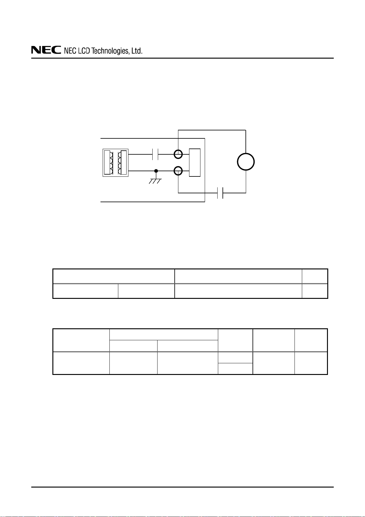
Note7: In case of Inverter with Ballast condenser, "VS" is the voltage level between Ballast condenser
and Connector (Refer to the below “Example of measurement”). "VS" should be designed to
be more than minimum "VS". Otherwise the lamp may not be turned on because the lamp
starting voltage is less than minimum "VS".
Example of measurement
Probe capacity: 3pF (Tektronix, inc. : P6015A)
Transformer
4.3.3 Power supply voltage ripple
This product works, even if the ripple voltage levels are beyond the permissible values as following
the table, but there might be noise on the display image.
Power supply voltage
Ballast condenser
Inverter
NL10276BC30-32D
(Lamp side)
Connector
Probe capacity
Ripple voltage Note1
(Measure at input terminal of power supply)
High voltage probe
VS
Unit
VCC 3.3V
≤ 100
Note1: The permissible ripple voltage includes spike noise.
4.3.4 Fuse
Parameter
Type Supplier
VCC FCC16202AB
Fuse
KAMAYA ELECTRIC
Co., Ltd
Rating Fusing current Remarks
2.0A
4.0A Note1
32V
Note1: The power supply capacity should be more than the fusing current. If it is less than the fusing
current, the fuse may not blow in a short time, and then nasty smell, smoke and so on may
occur.
mVp-p
DATA SHEET DOD-PP-1223 (5th edition)
10
Page 11
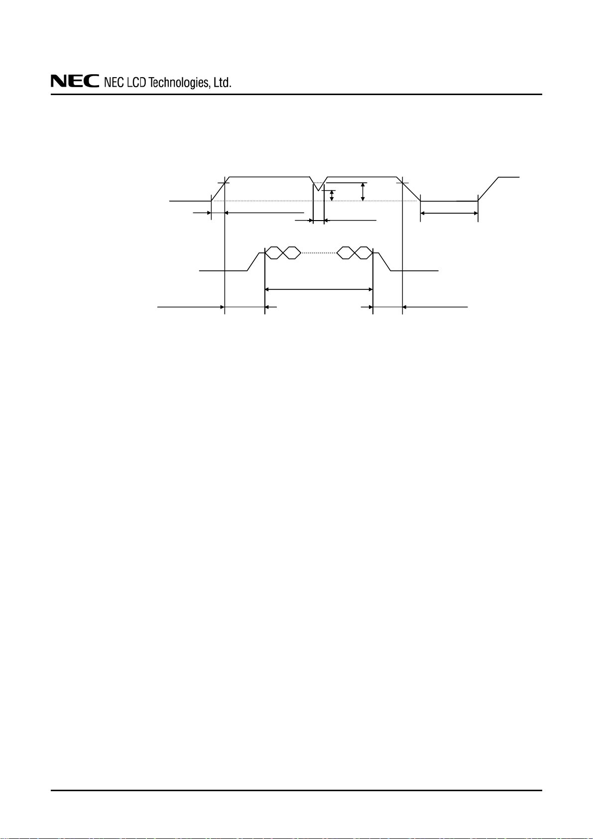
4.4 POWER SUPPLY VOLTAGE SEQUENCE
VCC
Note1
0V
ON OFF
3.0V
Display signals*,
Function signals
Note2
0.01ms < t < 50ms 0.01ms < t < 50ms
0V
* These signals should be measured at the terminal of 100Ω resistance.
Note1: In terms of voltage variation (voltage drop) while VCC rising edge is below 3.0V, a protection
circuit may work, and then this product may not work.
Note2: Display signals (D0+/ -, D1+/-, D2+/-, D3+/-, CLK+/-) and function signals (MSL, DPS) must
be Low or High impedance, exclude the VALID period (See above sequence diagram), in
order to avoid that internal circuit is damaged.
If some of display and function signals of this product are cut while this product is working,
even if the signal input to it once again, it might not work normally. VCC should be cut when
the display and function signals are stopped.
Note3: The backlight should be turned on within the valid perio d of display and function signals, in
order to avoid unstable data display.
0.1ms < Tr < 80ms
2.5V
20ms max.
VALID period
NL10276BC30-32D
ON
3.0V
Toff > 200ms
DATA SHEET DOD-PP-1223 (5th edition)
11
Page 12
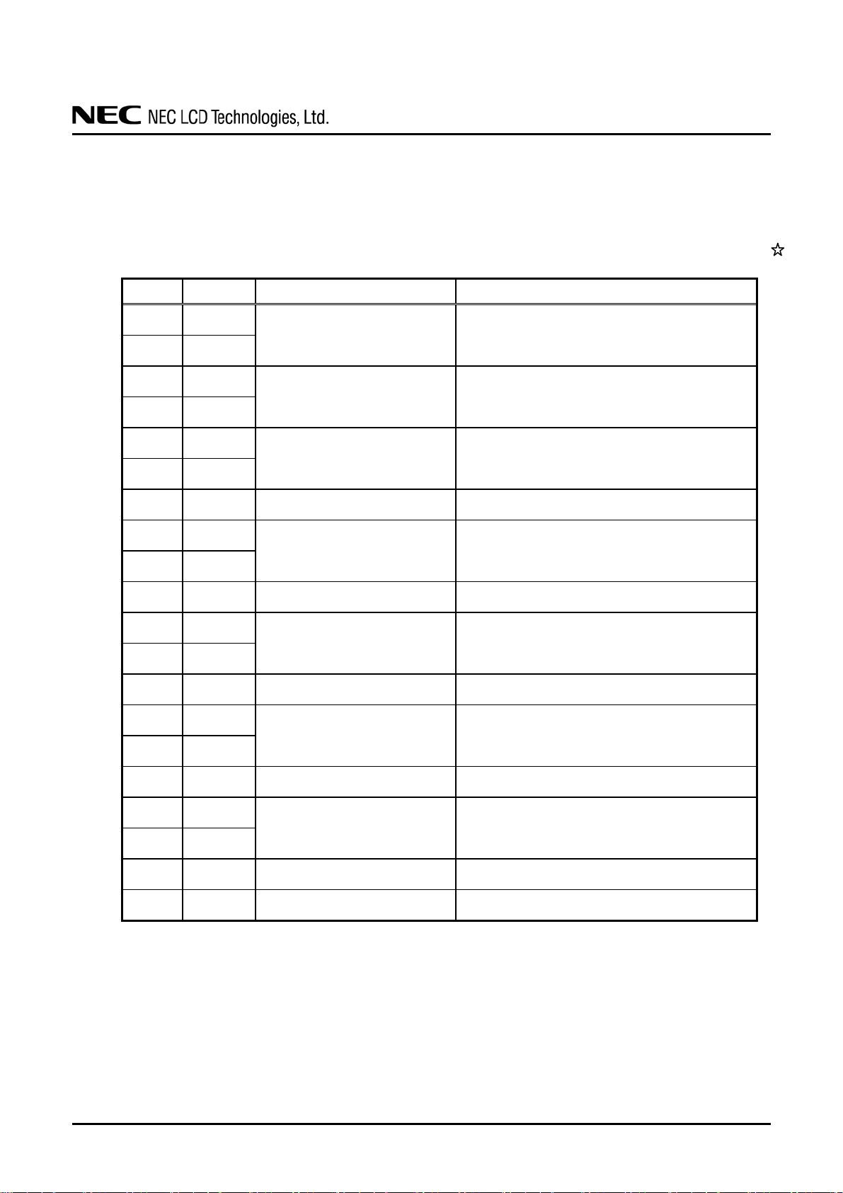
4.5 CONNECTIONS AND FUNCTIONS FOR INTERFACE PINS
4.5.1 LCD panel signal processing board
CN1 socket (LCD module side): DF14H-20P-1.25H (Hirose Electric Co., Ltd. (HRS))
MSB240420HE (SIN SHENG TERMINAL & MACHINE INC. (STM))
Adaptable plug: DF14-20S-1.25C (Hirose Electric Co., Ltd. (HRS))
Pin No. Symbol Signal Remarks
1 VCC
Power supply Note1
2 VCC
3 GND
Ground Note1
4 GND
5 D0-
Pixel data Note2
6 D0+
7 GND Ground Note1
NL10276BC30-32D
8 D1-
Pixel data Note2
9 D1+
10 GND Ground Note1
11 D2-
Pixel data Note2
12 D2+
13 GND Ground Note1
14 CLK-
Pixel clock Note2
15 CLK+
16 GND Ground Note1
17 D3-
Pixel data Note2
18 D3+
19 DPS Selection of scan direction
20 MSL Selection of LVDS input map
High: Reverse scan
Low or Open: Normal scan Note3, Note5
High: Input map A
Low or Open: Input map B Note4, Note5
Note1: All GND and VCC terminals should be used without any non-connected lines.
Note2: Twist pair wires with 100Ω (Characteristic impedance) should be used between LCD panel
signal processing board and LVDS transmitter.
Note3: See "4.8 SCANNING DIRECTIONS".
Note4: See "4.5.4 Connection between receiver and transmitter for LVDS".
Note5: This terminal is pulled-down in the product. (Pull-down resistance: 50kΩ)
DATA SHEET DOD-PP-1223 (5th edition)
12
Page 13
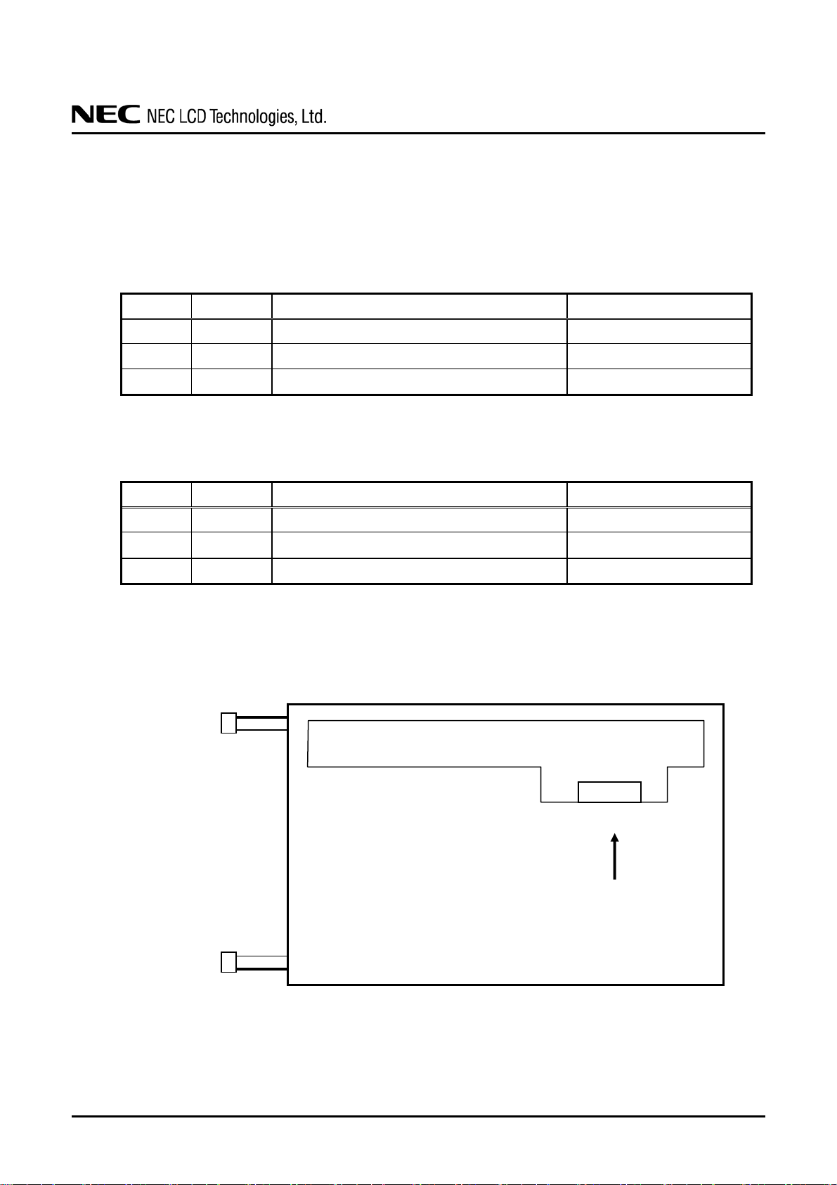
4.5.2 Backlight lamp
Attention: VBLH and VBLC must be connected correctly. Wrong connections will cause
CN201 plug (LCD module side): BHR-03VS-1 (J.S.T Mfg. Co., Ltd.)
Adaptable socket: SM02(8.0)B-BHS-1-TB(LF)(SN), SM02(8.0)B-BHS-1-TB
Pin No. Symbol Signal Remarks
CN202 plug (LCD module side): BHR-03VS-1 (J.S.T Mfg. Co., Ltd.)
Adaptable socket: SM02(8.0)B-BHS-1-TB(LF)(SN), SM02(8.0)B-BHS-1-TB
Pin No. Symbol Signal Remarks
NL10276BC30-32D
electric shock and also break down of the product.
(J.S.T Mfg. Co., Ltd.)
1 VBLH High voltage terminal (Hot) Cable color: Pink
2 N. C. - Keep this pin Open.
3 VBLC Low voltage terminal (Cold) Cable color: Gray
(J.S.T Mfg. Co., Ltd.)
1 VBLH High voltage terminal (Hot) Cable color: Pink
2 N. C. - Keep this pin Open.
3 VBLC Low voltage terminal (Cold) Cable color: Gray
4.5.3 Positions of plug and socket
CN201
1
3
CN202
3
1
Rear side
Signal processing board
CN1
20
1
Insert direction
DATA SHEET DOD-PP-1223 (5th edition)
13
Page 14
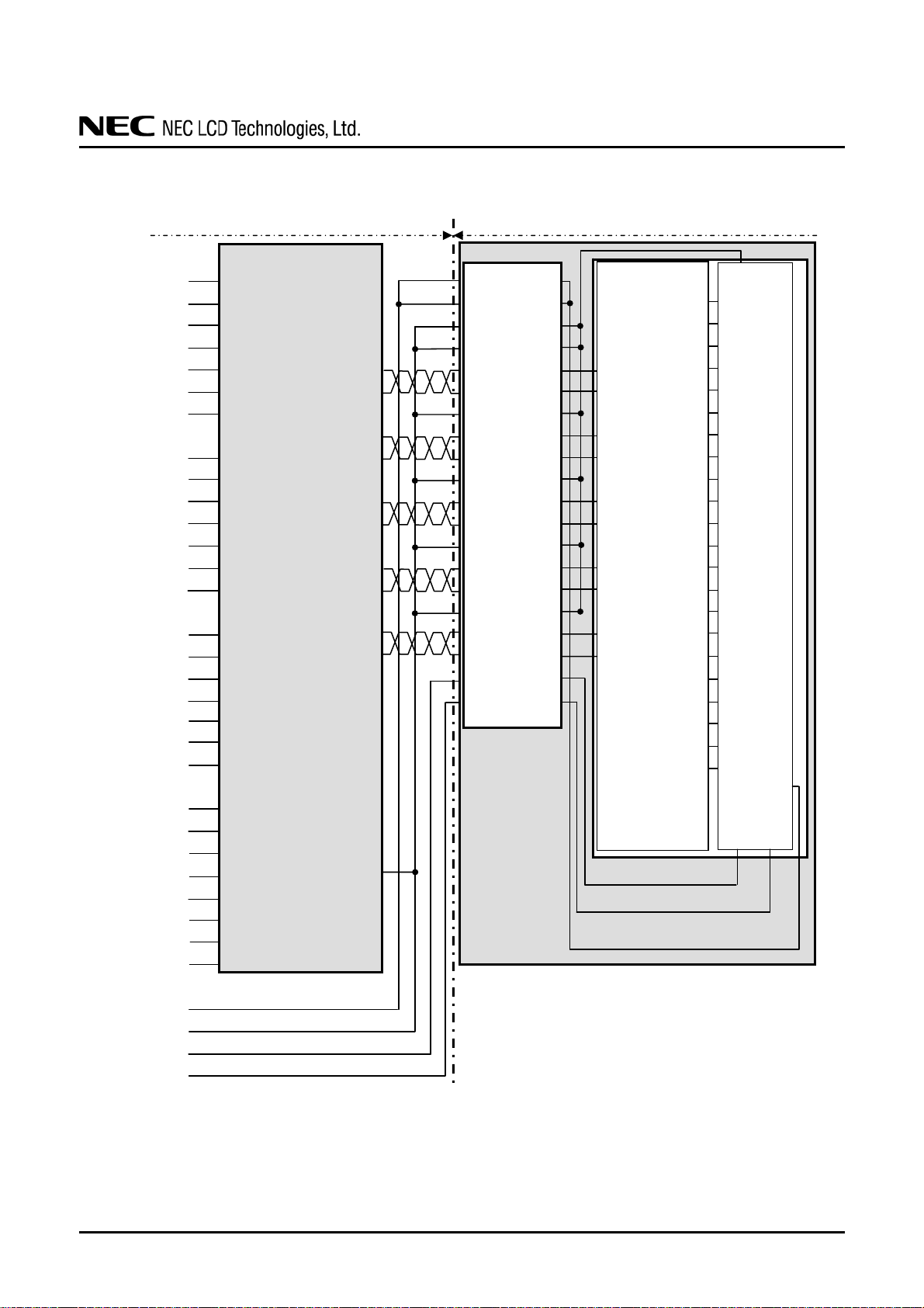
4.5.4 Connection between receiver and transmitter for LVDS (1) Input LVDS map A (MSL: "High")
Host
Note2
R2
R3
R4
R5
R6
R7
G2
G3
G4
G5
G6
G7
B2
B3
B4
B5
B6
B7
Note4
Note4
DE
R0
R1
G0
G1
B0
B1
Note4
CLK
VCC
GND
DPS
MSL (High)
Note3
TA0
TA1
TA2
TA3
TA4
TA5
TA6
TB0
TB1
TB2
TB3
TB4
TB5
TB6
TC0
TC1
TC2
TC3
TC4
TC5
TC6
TD0
TD1
TD2
TD3
TD4
TD5
TD6
CLK IN
LVDS transmitter
Note1
TA-
TA+
TB-
TB+
TC-
TC+
TCLK-
TCLK+
TD-
TD+
GND
Note1: Recommended transmitter: THC63LVDM83R (THine Electronics Inc.) or equivalent
Note2: LSB (Least Significant Bit) – R0, G0, B0 MSB (Most Significant Bit) – R7, G7, B7
Note3: Twist pair wires with 100Ω (Characteristic impedance) should be used between LCD panel
signal processing board and LVDS transmitter.
Note4: Input signals to TC4, TC5 and TD6 are not used inside the product, but do not keep TC4, TC5
and TD6 open to avoid noise problem.
1
2
3
4
5
6
7
8
9
10
11
12
13
14
15
16
17
18
19
20
VCC
VCC
GND
GND
D0D0+
GND
D1D1+
GND
D2-
D2+
GND
CLKCLK+
GND
D3D3+
DPS
MSL
CN1
NL10276BC30-32D
LCD module (Product)
RARA+
RBRB+
RCRC+
RCLKRCLK+
RDRD+
Receiver for LVDS
Equivalent of
THC63LVDF84B
DPS
LCD controller
LCD panel signal processing board
GND
Signal
processor
VCC
MSL
DATA SHEET DOD-PP-1223 (5th edition)
14
Page 15
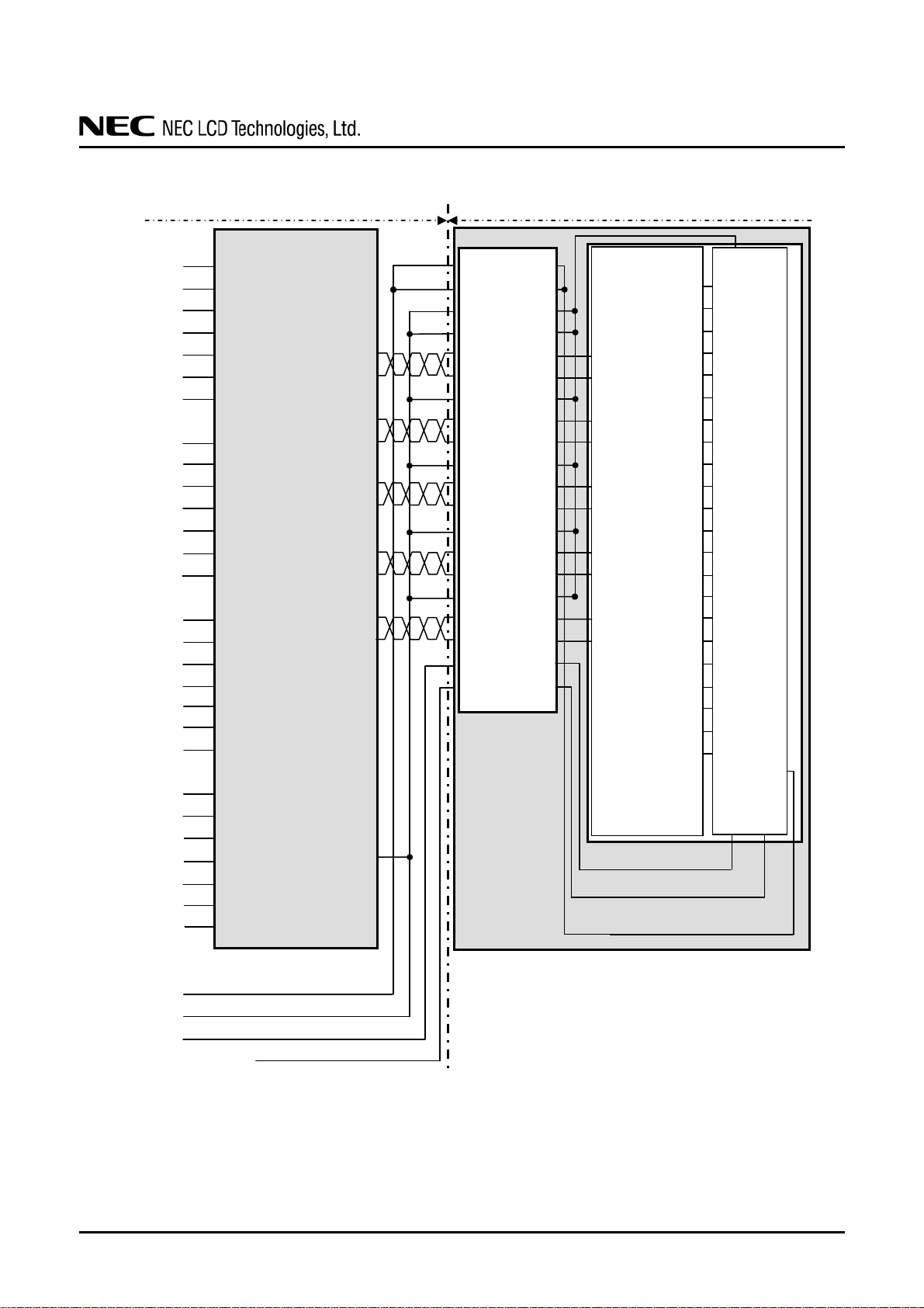
NL10276BC30-32D
(2) Input LVDS map B (MSL: "Low" or "Open")
Note2
R0
R1
R2
R3
R4
R5
G0
G1
G2
G3
G4
G5
B0
B1
B2
B3
B4
B5
Note4
Note4
DE
R6
R7
G6
G7
B6
B7
CLK
VCC
GND
DPS
MSL (Low or Open)
TXIN0
TXIN1
TXIN2
TXIN3
TXIN4
TXIN6
TXIN7
TXIN8
TXIN9
TXIN12
TXIN13
TXIN14
TXIN15
TXIN18
TXIN19
TXIN20
TXIN21
TXIN22
TXIN24
TXIN25
TXIN26
TXIN27
TXIN5
TXIN10
TXIN11
TXIN16
TXIN17
CLK IN
Host
TXOUT0-
TXOUT0+
TXOUT1-
TXOUT1+
TXOUT2-
TXOUT2+
TXCLKOUT-
TXCLKOUT+
TXOUT3-
TXOUT3+
LVDS transmitter
Note1
GND
Note3
10
11
12
13
14
15
16
17
18
19
20
VCC
1
VCC
2
GND
3
GND
4
D0-
5
D0+
6
GND
7
D1-
8
D1+
9
GND
D2-
D2+
GND
CLKCLK+
GND
D3D3+
DPS
MSL
CN1
Note1: Recommended transmitter: DS90C383 (National Semiconductor) or equivalent
Note2: LSB (Least Significant Bit) – R0, G0, B0 MSB (Most Significant Bit) – R7, G7, B7
Note3: Twist pair wires with 100Ω (Characteristic impedance) should be used between LCD panel
signal processing board and LVDS transmitter.
Note4: Input signals to TXIN24 and TXIN25 are not used inside the product, but do not keep TXIN24
and TXIN25 open to avoid noise problem.
LCD module (Product)
RARA+
RBRB+
RCRC+
RCLKRCLK+
RDRD+
Receiver for LVDS
Equivalent of
THC63LVDF84B
DPS
LCD controller
LCD panel signal processing board
GND
Signal
processor
VCC
MSL
DATA SHEET DOD-PP-1223 (5th edition)
15
Page 16
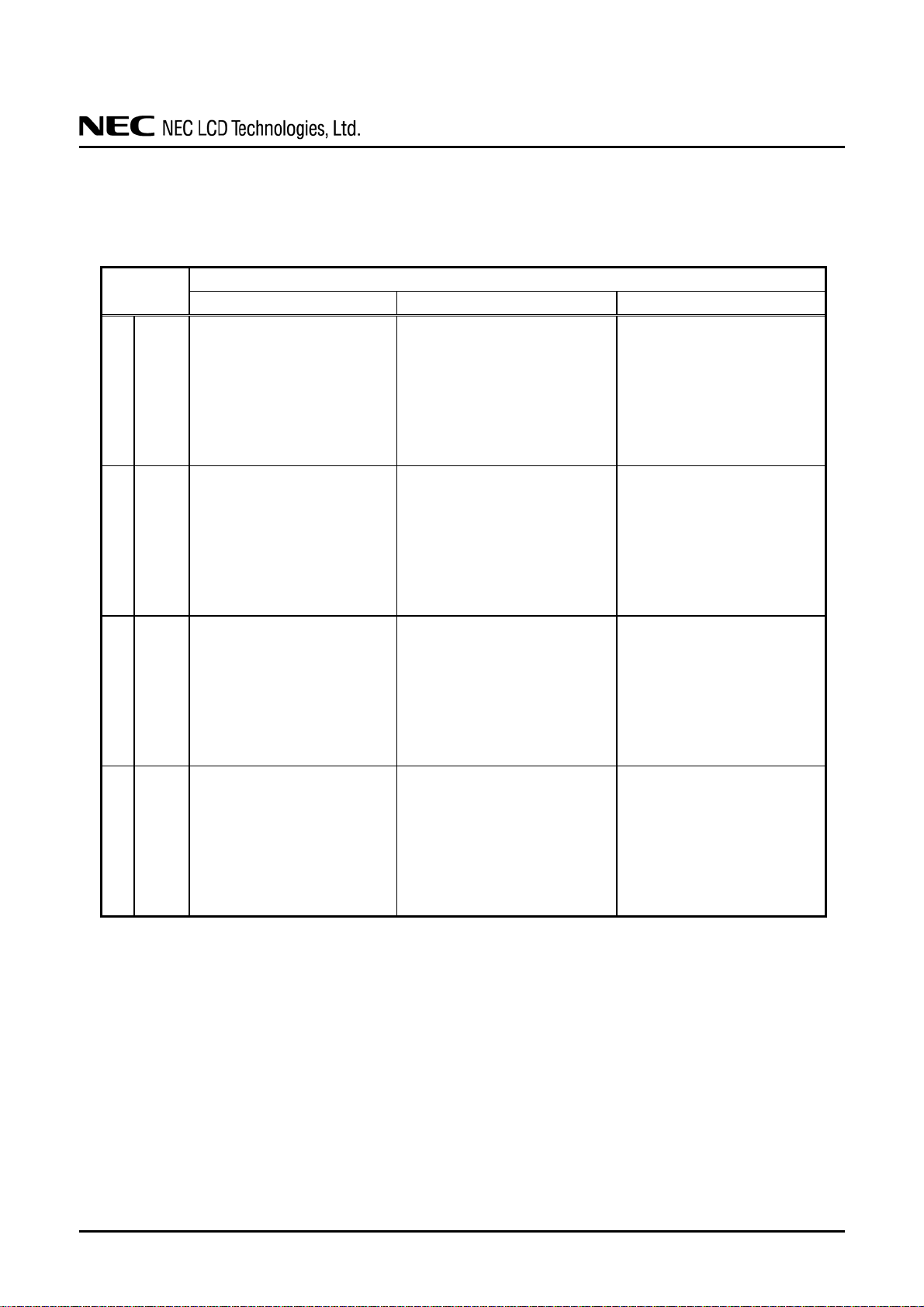
4.6 DISPLAY COLORS AND INPUT DATA SIGNALS
This product can display in equivalent to 16,777,216 colors in 256 gray scales. Also the relation
between display colors and input data signals is as the following table.
Display colors
Black
Blue
Magenta
Green
Cyan
Basic Colors
Yellow
White
Black
bright
Red gray scale
Black
bright
Green gray scale
Green
Black
bright
Blue gray scale
Blue
R7 R6 R5 R4 R3 R2 R1 R0 G7 G6 G5 G4 G3 G2 G1 G0 B7 B6 B5 B4 B3 B2 B1 B0
0 0 0 0 0 0 0 0
0 0 0 0 0 0 0 0
Red
1 1 1 1 1 1 1 1
1 1 1 1 1 1 1 1
0 0 0 0 0 0 0 0
0 0 0 0 0 0 0 0
1 1 1 1 1 1 1 1
1 1 1 1 1 1 1 1
0 0 0 0 0 0 0 0
0 0 0 0 0 0 0 1
dark
0 0 0 0 0 0 1 0
↑
↓
:
:
1 1 1 1 1 1 0 1
1 1 1 1 1 1 1 0
Red
1 1 1 1 1 1 1 1
0 0 0 0 0 0 0 0
0 0 0 0 0 0 0 0
dark
0 0 0 0 0 0 0 0
↑
↓
:
:
0 0 0 0 0 0 0 0
0 0 0 0 0 0 0 0
0 0 0 0 0 0 0 0
0 0 0 0 0 0 0 0
0 0 0 0 0 0 0 0
dark
0 0 0 0 0 0 0 0
↑
↓
:
:
0 0 0 0 0 0 0 0
0 0 0 0 0 0 0 0
0 0 0 0 0 0 0 0
Data signal (0: Low level, 1: High level)
0 0 0 0 0 0 0 0
0 0 0 0 0 0 0 0
0 0 0 0 0 0 0 0
0 0 0 0 0 0 0 0
1 1 1 1 1 1 1 1
1 1 1 1 1 1 1 1
1 1 1 1 1 1 1 1
1 1 1 1 1 1 1 1
0 0 0 0 0 0 0 0
0 0 0 0 0 0 0 0
0 0 0 0 0 0 0 0
:
:
0 0 0 0 0 0 0 0
0 0 0 0 0 0 0 0
0 0 0 0 0 0 0 0
0 0 0 0 0 0 0 0
0 0 0 0 0 0 0 1
0 0 0 0 0 0 1 0
:
:
1 1 1 1 1 1 0 1
1 1 1 1 1 1 1 0
1 1 1 1 1 1 1 1
0 0 0 0 0 0 0 0
0 0 0 0 0 0 0 0
0 0 0 0 0 0 0 0
:
:
0 0 0 0 0 0 0 0
0 0 0 0 0 0 0 0
0 0 0 0 0 0 0 0
NL10276BC30-32D
0 0 0 0 0 0 0 0
1 1 1 1 1 1 1 1
0 0 0 0 0 0 0 0
1 1 1 1 1 1 1 1
0 0 0 0 0 0 0 0
1 1 1 1 1 1 1 1
0 0 0 0 0 0 0 0
1 1 1 1 1 1 1 1
0 0 0 0 0 0 0 0
0 0 0 0 0 0 0 0
0 0 0 0 0 0 0 0
:
:
0 0 0 0 0 0 0 0
0 0 0 0 0 0 0 0
0 0 0 0 0 0 0 0
0 0 0 0 0 0 0 0
0 0 0 0 0 0 0 0
0 0 0 0 0 0 0 0
:
:
0 0 0 0 0 0 0 0
0 0 0 0 0 0 0 0
0 0 0 0 0 0 0 0
0 0 0 0 0 0 0 0
0 0 0 0 0 0 0 1
0 0 0 0 0 0 1 0
:
:
1 1 1 1 1 1 0 1
1 1 1 1 1 1 1 0
1 1 1 1 1 1 1 1
DATA SHEET DOD-PP-1223 (5th edition)
16
Page 17
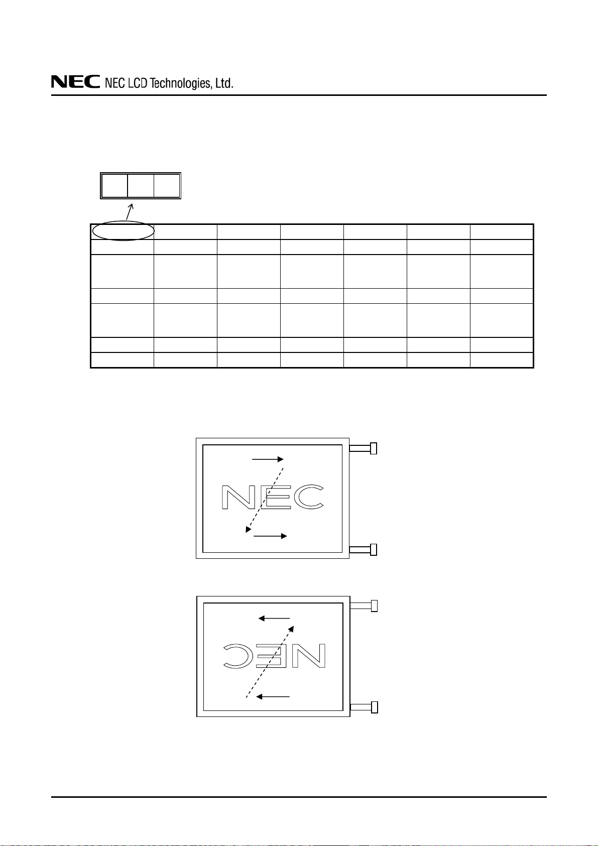
4.7 DISPLAY POSITIONS
The following table is the coordinates per pixel (See "4.8 SCANNING DIRECTIONS".).
C (0, 0)
R G B
C( 0, 0) C( 1, 0)
C( 0, 1) C( 1, 1)
•
•
•
C( 0, Y) C( 1, Y)
•
•
•
C( 0, 766) C( 1, 766)
C( 0, 767) C( 1, 767)
4.8 SCANNING DIRECTIONS
The following figures are seen from a front view. Also the arrow shows the direction of scan.
Note1: Meaning of C (X, Y) and D (X, Y)
C (X, Y): The coordinates of the display position (See "4.7 DISPLAY POSITIONS".)
D (X, Y): The data number of input signal for LCD panel signal processing board
C( X, 0)
C( X, 1)
•
•
•
C( X, Y)
•
•
•
C( X, 766)
C( X, 767)
C (1023, 0)
D (1023, 0)
C (1023, 767)
D (1023, 767)
•
•
•
•
•
•
• • •
• • •
•
• • •
•
• • •
•
• • •
•
• • •
• • •
C (0, 0)
D (0, 0)
C (0, 767)
D (0, 767)
Figure1. Normal scan (DPS: Low or Open)
C (0, 0)
D (1023, 767)
C (0, 767)
D (1023, 0)
C (1023, 0)
D (0, 767)
C (1023, 767)
D (0, 0)
Figure2. Reverse scan (DPS: High)
• • •
• • •
•
• • •
•
• • •
•
• • •
•
• • •
• • •
Note1
Note1
NL10276BC30-32D
C(1022, 0) C(1023, 0)
C(1022, 1) C(1023, 1)
•
•
•
C(1022, Y) C(1023, Y)
•
•
•
C(1022, 766) C(1023, 766)
C(1022, 767) C(1023, 767)
•
• • •
•
•
•
•
DATA SHEET DOD-PP-1223 (5th edition)
17
Page 18
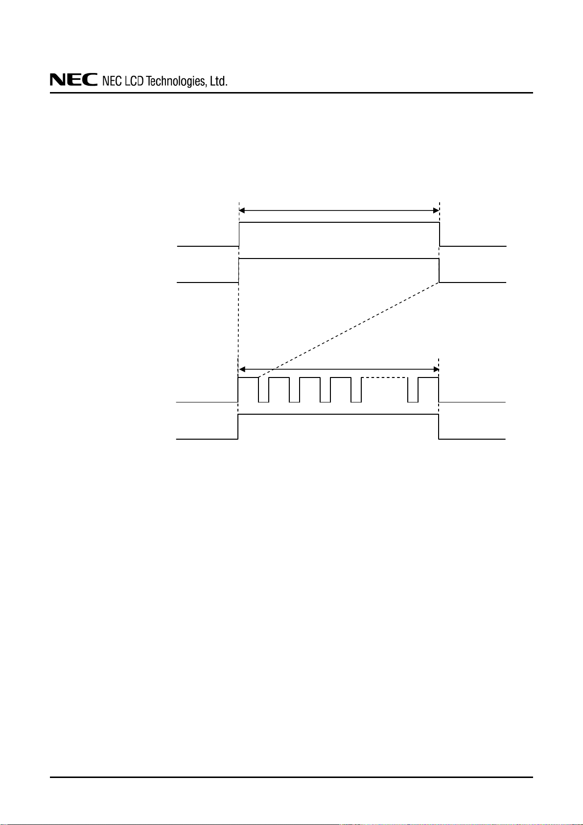
4.9 INPUT SIGNAL TIMINGS
4.9.1 Outline of input signal timings
• Horizontal signal
Note1
DE (Data enable)
Display period
• Vertical signal
Note1
DE (Data enable)
Display period
Note1: This diagram indicates virtual signal for set up to timing.
Note2: See "4.9.3 Input signal timing chart" for numeration of pulse.
NL10276BC30-32D
Horizontal display period (thd)
Vertical display period (tvd)
1
2
34
768
Note2
DATA SHEET DOD-PP-1223 (5th edition)
18
Page 19
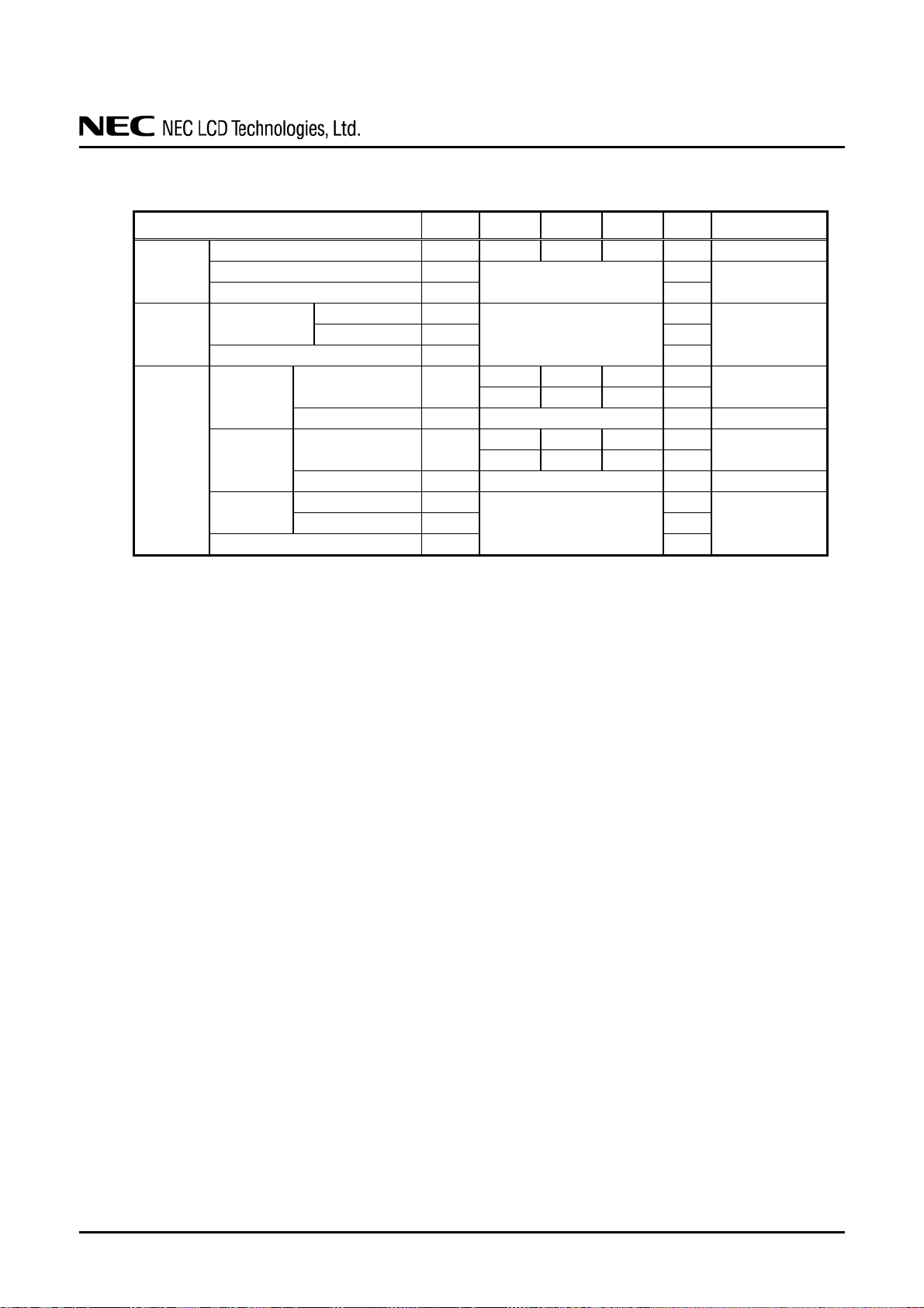
4.9.2 Timing characteristics
CLK
DATA
DE
Note1: Definition of parameters is as follows.
Note2: See the data sheet of LVDS transmitter.
Note3: Vertical cycle (tv) should be specified in integral multiple of Horizontal cycle (th).
NL10276BC30-32D
(Note1, Note2, Note3)
Parameter Symbol min. typ. max. Unit Remarks
Frequency 1/tc 50.0 65.0 80.0 MHz 15.384 ns (typ.)
Duty - -
Rise time, Fall time -
CLK-DATA
Rise time, Fall time -
Horizontal
Vertical
(One frame)
CLK-DE
Rise time, Fall time -
Setup time - ns
Hold time - ns
Cycle th
Display period thd 1,024 CLK -
Cycle tv
Display period tvd 768 H -
Setup time - ns
Hold time - ns
tc= 1CLK, th= 1H, Vf= 1/tv
15 20.676 -
1,050 1,344 1,800 CLK
13.1 16.666 20.0 ms
770 806 - H
-
-
-
ns
ns
μs
48.363 kHz (typ.)
ns
-
-
60.000 Hz (typ.)
-
DATA SHEET DOD-PP-1223 (5th edition)
19
Page 20
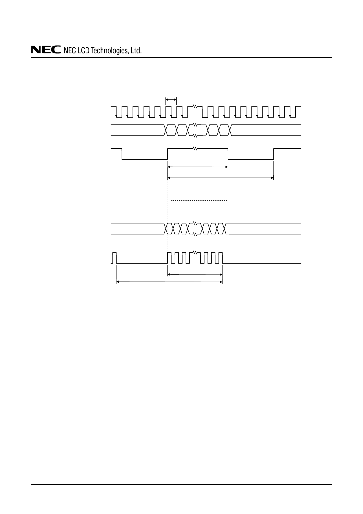
4.9.3 Input signal timing chart
Horizontal timing
CLK
DATA
(R0-R7)
(G0-G7)
(B0-B7)
DE
Vertical timing
DATA
(R0-R7)
(G0-G7)
(B0-B7)
DE
tc
Invalid
Invalid I
1 2 1023 1024
thd
th
1 2 767 768
tvd
tv
NL10276BC30-32D
Invalid
nvalid
DATA SHEET DOD-PP-1223 (5th edition)
20
Page 21
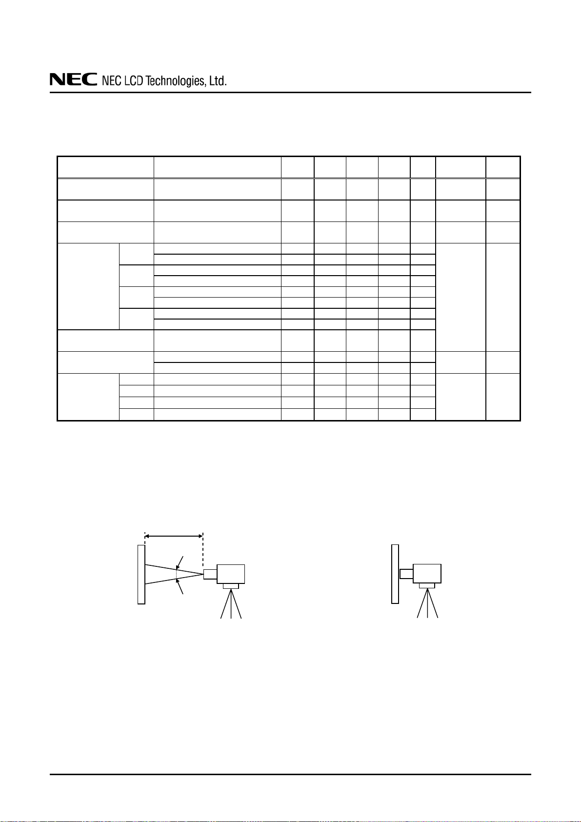
4.10 OPTICS
4.10.1 Optical characterist ics
Parameter Condition Symbol min. typ. max. Unit
Luminance
Contrast ratio
Luminance uniformity
White
Red
Chromaticity
Green
Blue
Color gamut
Response time
Right
Viewing angle
Left
Up
Down
Note1: These are initial characteristics.
Note2: Measurement conditions are as follows.
Ta= 25°C, VCC= 3.3V, IBL= 7.5mArms/lamp, Display mode: XGA,
Horizontal cycle= 1/48.363kHz, Vertical cycle= 1/60.0Hz, DPS= Low or Open: Normal scan
Optical characteristics are measured at luminance saturation after 20minutes from working the
product, in the dark room. Also measurement methods are as follows.
LCD module
(Product)
Note3: See "4.10.2 Definition of contrast ratio".
Note4: See "4.10.3 Definition of luminance uniformity".
Note5: These coordinates are found on CIE 1931 chromaticity diagram.
Note6: Product surface temperature: TopF= 32°C
Note7: See "4.10.4 Definition of response times".
Note8: See "4.10.5 Definition of viewing angles".
White at center
θR= 0°, θL= 0°, θU= 0°, θD= 0°
White/Black at center
θR= 0°, θL= 0°, θU= 0°, θD= 0°
White
θR= 0°, θL= 0°, θU= 0°, θD= 0°
x coordinate Wx 0.283 0.313 0.343 y coordinate Wy 0.299 0.329 0.359 x coordinate Rx - 0.62 - y coordinate Ry - 0.35 - x coordinate Gx - 0.32 - y coordinate Gy - 0.57 - x coordinate Bx - 0.15 - y coordinate By - 0.12 - -
θR= 0°, θL= 0°, θU= 0°, θD= 0°
at center, against NTSC color space
White to Black Ton - 4 8 ms
Black to White Toff - 14 22 ms
θU= 0°, θD= 0°, CR≥ 10 θR
θU= 0°, θD= 0°, CR≥ 10 θL
θR= 0°, θL= 0°, CR≥ 10 θU
θR= 0°, θL= 0°, CR≥ 10 θD
50cm
1°
Photodetector (BM-5A or SR-3)
NL10276BC30-32D
(Note1, Note2)
Measuring
instrument
SR-3 or
L 200 250 - cd/m
CR 350 500 - -
LU - 1.2 1.35 - BM-5A Note4
C 40 50 - %
70 80 70 80 70 80 70 80 -
LCD module
(Product)
2
BM-5A
SR-3 or
BM-5A
SR-3 Note5
BM-5A
°
BM-5A or
°
°
°
Photodetector (EZ Contrast)
EZ
Contrast
Remarks
-
Note3
Note6
Note7
Note8
DATA SHEET DOD-PP-1223 (5th edition)
21
Page 22
①
②
N
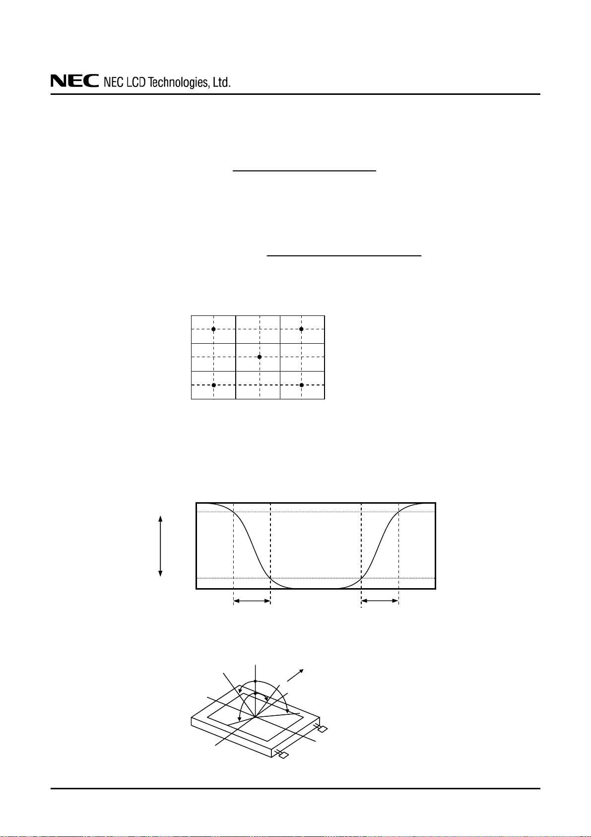
4.10.2 Definition of contrast ratio
The contrast ratio is calculated by using the following formula.
Contrast ratio (CR) =
4.10.3 Definition of luminance uniformity
The luminance uniformity is calculated by using following formula.
Luminance uniformity (LU) =
The luminance is measured at near the 5 points shown below.
128
384
640
4.10.4 Definition of response times
Response time is measured, the luminance changes from "white" to "black", or "black" to "white"
on the same screen point, by photo-detector. Ton is the time it takes the luminance change from
90% down to 10%. Also Toff is the time it takes the luminance change from 10% up to 90% (See
the following diagram.).
White
100%
90%
Luminance
Black
10%
0%
4.10.5 Definition of viewing angles
Left
Luminance of white screen
Luminance of black screen
Maximum luminance from ①
Minimum luminance from ①
171 512 853
③
④
Ton
ormal axis (Perpendicular)
θL
θU
θD
Lower
Upper
NL10276BC30-32D
to ⑤
to ⑤
⑤
Toff
12 o’clock
θR
Right
DATA SHEET DOD-PP-1223 (5th edition)
22
Page 23
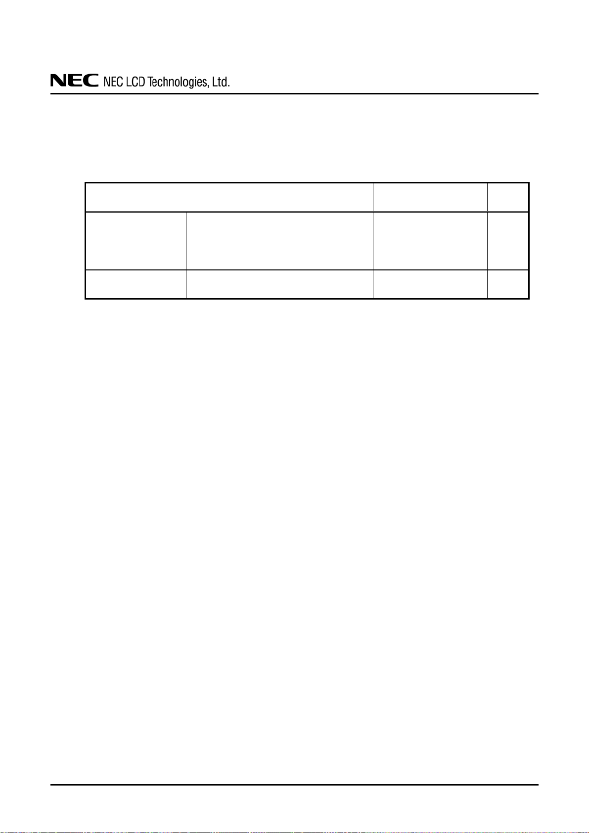
5. ESTIMATED LUMINANCE LIFETIME
The luminance lifetime is the time from initial luminance to half-luminance.
This lifetime is the estimated value, and is not guarantee value.
Condition
NL10276BC30-32D
Luminance lifetime (MTTF)
Note1, Note2
Unit
Module
Cold cathode fluorescent
lamp
25°C (Ambient temperature of the product)
Continuous operation, IBL= 7.5mArms/lamp
70°C (Surface temperature at screen center)
Continuous operation, IBL= 7.5mArms/lamp
25°C (Ambient temperature of the lamp)
Continuous operation, IBL= 7.5mArms
40,000 h
30,000 h
50,000 h
Note1: MTTF is mean time to half-luminance.
Note2: In case the product works under low temperature environment, the lifetime becomes short.
DATA SHEET DOD-PP-1223 (5th edition)
23
Page 24
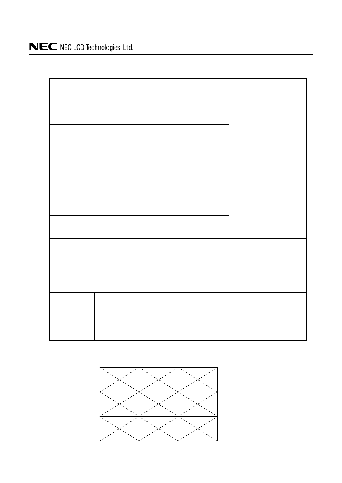
6. RELIABILITY TESTS
Test item Condition Judgment Note1
NL10276BC30-32D
High temperature and humidity
(Operation)
High temperature
(Operation)
Heat cycle
(Operation)
Thermal shock
(Non operation)
ESD
(Operation)
Dust
(Operation)
Vibration
(Non operation)
Mechanical shock
(Non operation)
① 60 ± 2°C, RH= 90%, 240hours
② Display data is black.
① 70 ± 3°C, 240hours
② Display data is black.
① -20 ± 3°C…1hour
70 ± 3°C…1hour
② 50cycles, 4hours/cycle
③ Display data is black.
① -20 ± 3°C…30minutes
80 ± 3°C…30minutes
② 100cycles, 1hour/cycle
③ Temperature transition time is within 5
minutes.
① 150pF , 150Ω, ±10kV
② 9 places on a panel surface Note2
③ 10 times each places at 1 sec interval
① Sample dust: No. 15 (by JIS-Z8901)
② 15 seconds stir
③ 8 times repeat at 1 hour interval
① 5 to 100Hz, 11.76m/s
② 1 minute/cycle
③ X, Y , Z directions
④ 50 times each directions
2
① 294m/s
② X, Y , Z directions
③ 3 times each directions
, 11ms
2
No display malfunctions
No display malfunctions
No physical damages
① 53.3kPa (Equivalent to altitude 4,850m)
Operation
Low pressure
Non-operation
② -20°C±3°C…24 hours
③ 70°C±3°C…24 hours
No display malfunctions
① 15kPa (Equivalent to altitude 13,600m)
② -20°C±3°C…24 hours
③ 80°C±3°C…24 hours
Note1: Display and appearance are checked under environmental conditions equivalent to the
inspection conditions of defect criteria.
Note2: See the following figure for discharge points.
{ {
{
{
{
{
{
{
{
DATA SHEET DOD-PP-1223 (5th edition)
24
Page 25
!
7. PRECAUTIONS
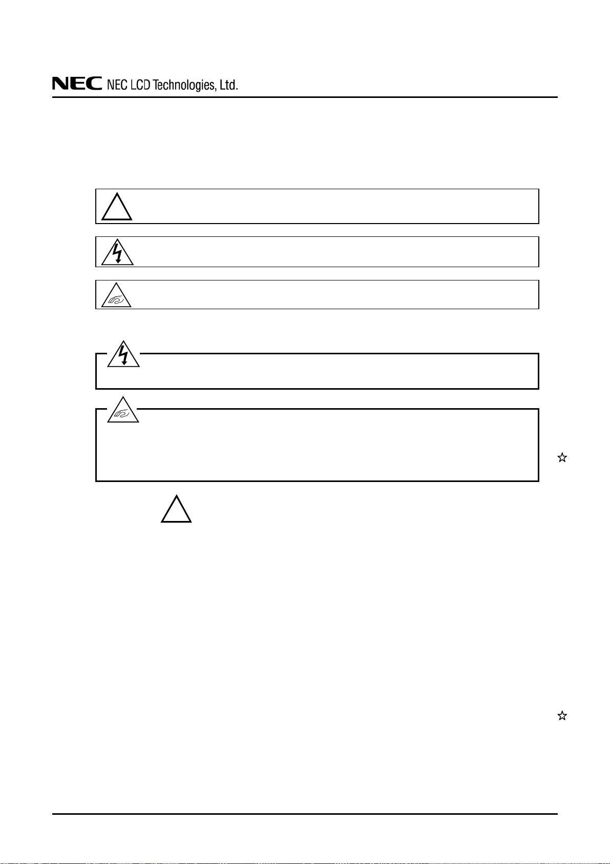
7.1 MEANING OF CAUTION SIGNS
The following caution signs have very important meaning. Be sure to read "7.2 CAUTIONS" and
"7.3 ATTENTIONS", after understanding these contents!
This sign has the meaning that customer will be injured by himself or the product will
!
7.2 CAUTIONS
∗ Do not touch the working backlight. There is a danger of an electric shock.
sustain a damage, if customer has wrong operations.
This sign has the meaning that customer will get an electrical shock, if customer has
wrong operations.
This sign has the meaning that customer will be injured by himself, if customer has
wrong operations.
NL10276BC30-32D
∗ Do not touch the working backlight. There is a danger of burn injury.
∗ Do not shock and press the LCD panel and the backlight! There is a danger of breaking,
because they are made of glass. (Shock: Equal to or no greater than 294m/s
to or no greater than 11ms, Pressure: Equal to or no greater than 19.6 N (φ16mm jig))
7.3 A TTENTIONS
7.3.1 Handling of the product
① Take hold of both ends without touching the circuit board when the product (LCD module) is
picked up from inner packing box to avoid broken down or misadjustment, because of stress to
mounting parts on the circuit board.
② Do not hook nor pull cables such as lamp cable, and so on, in order to avoid any damage.
③ When the product is put on the table temporarily, display surface must be placed downward.
④ When handling the product, take the measures of electrostatic discharge with such as earth band,
ionic shower and so on, because the product may be damaged by electrostatic.
⑤ The torque for product mounting screws must never exceed 0.343N⋅m. Higher torque might result
in distortion of the bezel. And the length of product mounting screws must be ≤ 2.8mm.
⑥ The product must be installed using mounting holes without undue stress such as bends or twist
(See outline drawings). And do not add undue stress to any portion (such as bezel flat area). Bends
or twist described above and undue stress to any portion may cause display mura.
⑦ Do not press or rub on the sensitive product surface. When cleaning the product surface, wipe it
with a soft dry cloth.
⑧ Do not push nor pull the interface connectors while the product is working.
⑨ Do not bend or unbend the lamp cable at the near part of the lamp holding rubber, to avoid the
damage for high voltage side of the lamp.
2
and equal
DATA SHEET DOD-PP-1223 (5th edition)
25
Page 26

⑩ Properly connect the plug (backlight side) to adaptable socket (inverter side) without incomplete
⑪ If the lamp cable is attached on the metal part of the product directly, high frequency leak current
⑫ When handling the product, use of an original protection sheet on the product surface (polarizer) is
⑬ Usually liquid crystals don't leak through the breakage of glasses because of the surface tension of
7.3.2 Environment
① Do not operate or store in high temperature, high humidity, dewdrop atmosphere or corrosive gases.
② In order to prevent dew condensation occurring by temperature difference, the product packing box
③ Do not operate in high magnetic field. Circuit boards may be broken down by it.
④ This product is not designed as radiation hardened.
7.3.3 Characteristics
The following items are neither defects nor failures.
① Response time, luminance and color may be changed by ambient temperature.
② Display mura, flicker, vertical seam or small spot may be observed depending on display patterns.
③ Optical characteristics (e.g. luminance, display uniformity, etc.) gradually is going to change
④ Do not display the fixed pattern for a long time because it may cause image sticking. Use a screen
⑤ The display color may be changed depending on viewing angle because of the use of condenser
⑥ Optical characteristics may be changed depending on input signal timings.
⑦ The interference noise between input signal frequency for this product's signal processing board
⑧ After the product is stored under condition of low temperature or dark place for a long time, the
NL10276BC30-32D
connection. After connecting, be careful not to hook the lamp cables because incomplete
connection may occur by hooking the lamp cables. This incomplete connection may cause
abnormal operation of high voltage circuit.
to the metal part may occur, then the brightness may decrease or the lamp may not be turned on.
recommended for protection of product surface. Adhesive type protection sheet may change color
or characteristics of the polarizer.
thin layer and the construction of LCD panel. But, if you contact with liquid crystal for the worst,
please wash it out with soap.
Keep the product in packing box with antistatic pouch in room temperature to avoid dusts and
sunlight, when storing the product.
should be opened after enough time being left under the environment of an unpacking room.
Evaluate the leaving time sufficiently because a situation of dew condensation occurring is
changed by the environmental temperature and humidity. (Recommended leaving time: 6 hours or
more with packing state)
depending on operating time, and especially low temperature, because the LCD has cold cathode
fluorescent lamps.
saver, if the fixed pattern is displayed on the screen.
sheet in the backlight.
and luminance control frequency of the inverter may appear on a display. Set up luminance control
frequency of the inverter so that the interference noise does not appear.
cold cathode fluorescent lamp may not be turned on under the same condition because of the
general characteristic of cold cathode fluorescent lamp. In addition, when Luminance control ratio
is low in pulse width modulation method inverter, the lamp may not be turned on. In this case,
power should be supplied again.
DATA SHEET DOD-PP-1223 (5th edition)
26
Page 27
NL10276BC30-32D
7.3.4 Other
① All GND and VCC terminals should be used without any non-connected lines.
② Do not disassemble a product or adjust variable resistors.
③ See "REPLACEMENT MANUAL FOR LAMP HOLDER SET", when replacing backlight lamps.
④ Pack the product with original shipping package, in order to avoid any damages during
transportation, when returning the product to NEC for repair and so on.
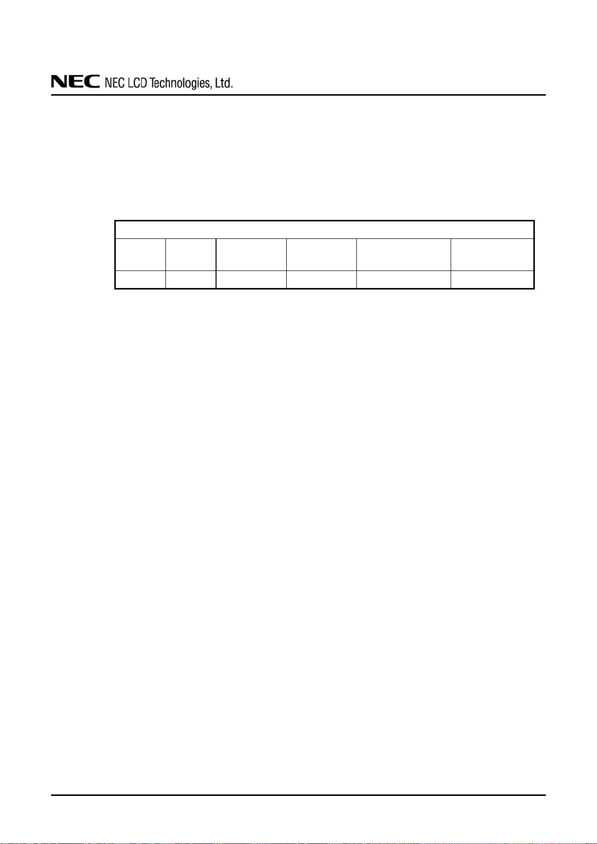
⑤ The information of China RoHS directive six hazardous substances or elements in this product is
as follows.
China RoHS directive six hazardous substances or elements
Lead
(Pb)
✕ ✕
Mercury
(Hg)
Cadmium
(Cd)
Hexavalent
Chromium
(Cr VI)
Note1: : This indicates that the poisonous or harmful material in all the homogeneous materials
for this part is equal or below the limitation level of SJ/T11363-2006 standard
regulation.
✕: This indicates that the poisonous or harmful material in all the homogeneous
materials for this part is above the limitation level of SJ/T11363-2006 standard
regulation.
Polybrominated
Biphenys
(PBB)
Polybrominated
Biphenyl Ethers
(PBDE)
DATA SHEET DOD-PP-1223 (5th edition)
27
Page 28
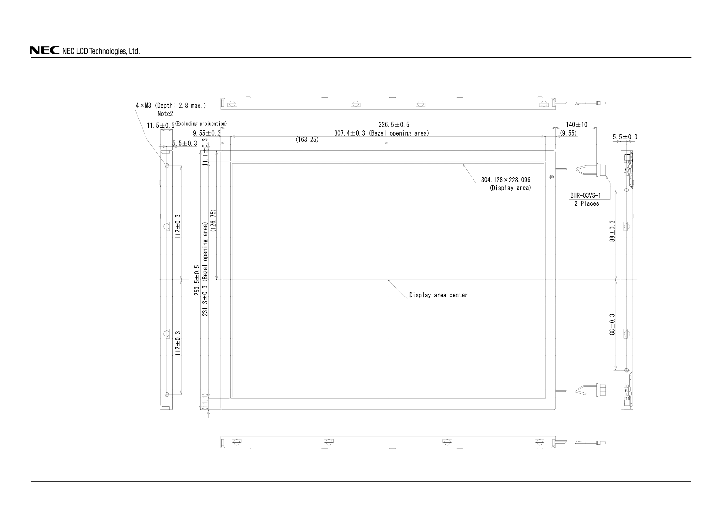
8. OUTLINE DRAWINGS
8.1 FRONT VIEW
Note1: The values in parentheses are for reference.
Note2: The torque for product mounting screws must never exceed 0.343N⋅m. And the length of product mounting screws must be ≤ 2.8mm..
NL10276BC30-32D
Unit: mm
DATA SHEET DOD-PP-1223 (5th edition)
28
Page 29
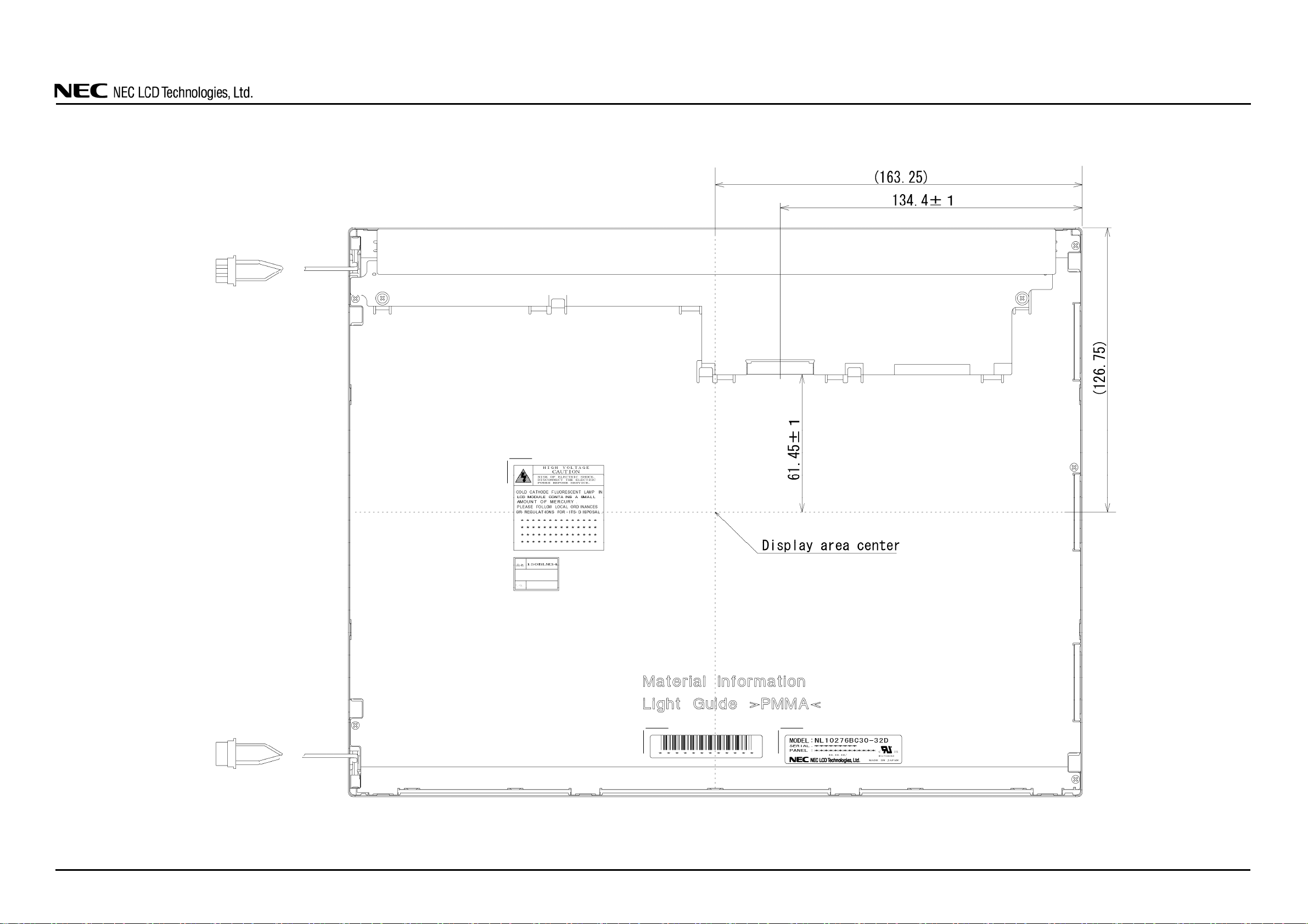
8.2 REAR VIEW
NL10276BC30-32D
Unit: mm
Note1: The values in parentheses are for reference.
DATA SHEET DOD-PP-1223 (5th edition)
29
 Loading...