

NEC NE6500379A, NE6500379A-T1 Datasheet
DATA SHEET
N-CHANNEL GaAs MES FET
NE6500379A
3W L, S-BAND POWER GaAs MESFET
DESCRIPTION
The NE6500379A is a 3W GaAs MESFET designed for middle power transmitter applications for mobile
communication handset and base station systems. It is capable of delivering 3 watt of output power (CW) with high
linear gain, high efficiency and excellent distortion. Reliability and performance uniformity are assured by NEC’s
stringent quality and control procedures.
FEATURES
• High Output Power : P
• High Linear Gain : 10 dB typ.
• High Power Added Efficiency: 50% typ. @VDS = 6 V, I
o (1dB)
= +35 dBm typ.
Dset
= 500 mA, f = 1.9 GHz
ORDERING INFORMATION
Part Number Package Supplying Form
NE6500379A-T1 79A 12 mm tape width, 1 kpcs / reel
Remark
To order evaluation samples, please contact your local NEC sales office.
(Part number for sample order: NE6500379A)
ABSOLUTE MAXIMUM RATINGS (TA = 25°C)
Operation in excess of any one of these parameters may result in permanent damage.
Parameter Symbol Ratings Unit
Drain to Source Voltage V
Gate to Source Voltage V
Drain Current I
Gate Current I
Total Power Dissipat i on P
Channel Temperature T
Storage Temperature T
DS
GSO
D
G
ch
stg
15 V
–7 V
5.6 A
50 mA
T
21 W
150 °C
–65 to +150 °C
Caution Please handle this device at static-free workstation, because this is an electrostatic sensitive
device.
Document No. P13495EJ2V0DS00 (2nd edition)
Date Published August 1998 N CP(K)
Printed in Japan
The information in this document is subject to change without notice.
The mark shows major revised points.
1998©
RECOMMENDED OPERATING LIMITS
Characteristics Symbol Test Condi tions MIN. TYP. MAX. Unit
NE6500379A
Drain to Source Voltage V
DS
6.0 6.0 V
Gain Compression Gcomp 3.0 dB
Channel Temperature T
ch
+125 °C
ELECTRICAL CHARACTERISTICS
(TA = 25°C, Unless otherwise specified, using NEC standard test fixture.)
Characteristics Symbol Test Condi tions MIN. TYP. MAX. Unit
P
BV
o(1dB)
η
G
DSS
add
VDS = 2.5 V, VGS = 0 V 4.5 A
p
VDS = 2.5 V, ID = 21 mA –3.6 –1.6 V
gd
Igd = 21 mA 17 V
th
Channel to Case 5 6 °C/W
f = 1.9 GHz, VDS = 6.0 V
35.0 dBm
Rg = 30 Ω
D
Dset
I
= 500 mA (RF OFF)
Note 2
L
9.0 10.0 dB
1.0 A
50 %
Saturated Drain Current I
Pinch-off Voltage V
Gate to Drain Break Down
Voltage
Thermal Resistance R
Output Power at 1 dB Gain
Compression Point
Drain Current I
Power Added Efficiency
Linear Gain
Note 1
Notes 1.
Pin = 0 dBm
DC performance is 100% testing. RF performance is testing several samples per wafer.
2.
Wafer rejection criteria for standard devices is 1 reject for several samples.
2
NE6500379A
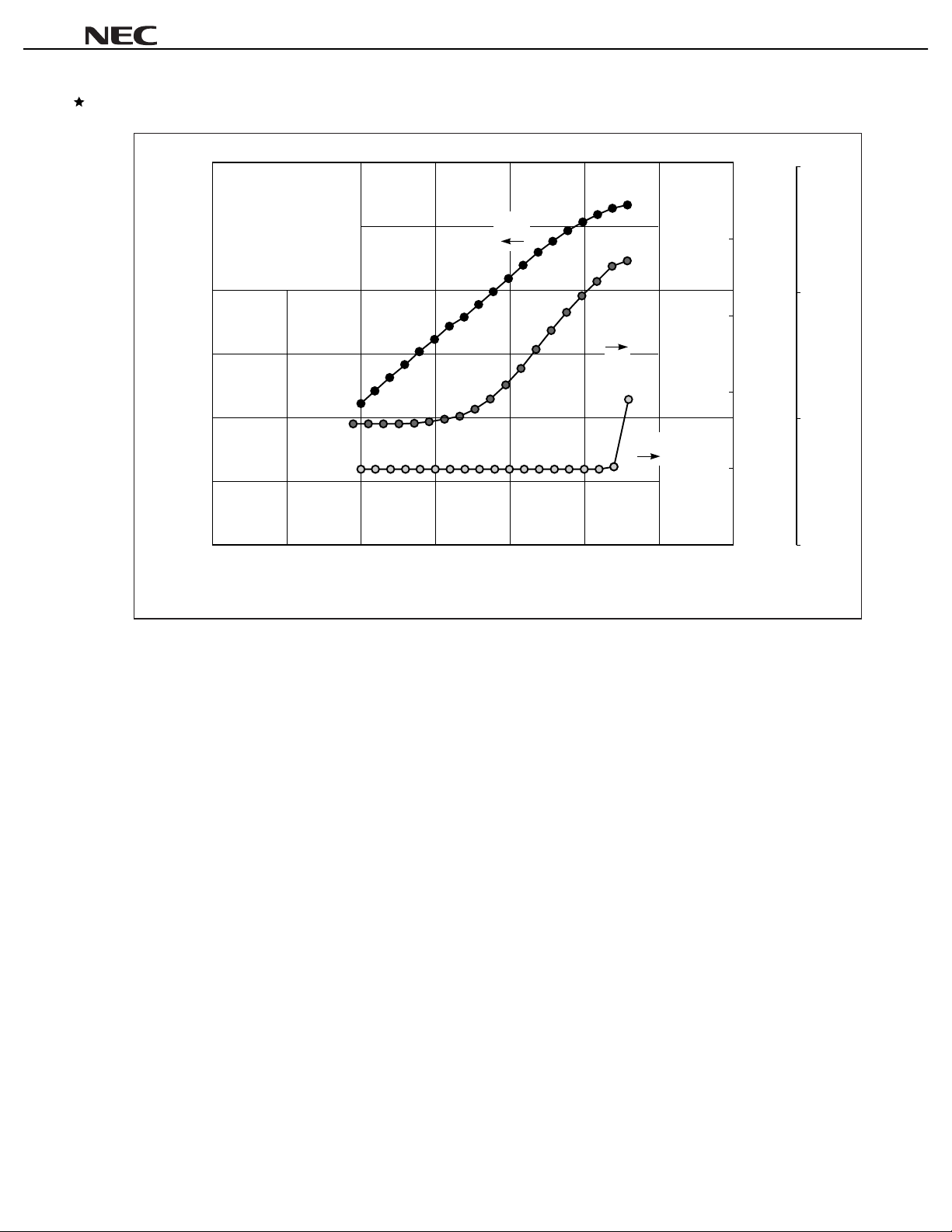
OUTPUT POWER, DRAIN CURRENT AND GATE CURRENT vs. INPUT POWER
40
35
30
25
Pout [dBm]
20
15
10
VDS = 6 V
I
Dset
= 500 mA (RF OFF)
R
g
= 30 Ω
f = 1.9 GH
0
20
Z
Pout
15
1500
1000
10
I
D
[mA]
G
I
[mA]
D
I
5
500
I
G
0
–5
30252015105
35
0
Pin [dBm]
3
 Loading...