


DATA SHEET
*
MOS INTEGRATED CIRCUIT
µ
PD754144, 754244
4-BIT SINGLE-CHIP MICROCONTROLLERS
DESCRIPTION
The µPD754244 is a 4-bit single-chip microcontroller which incorporates the EEPROMTM for key-less entry
application.
It incorporates a 16 × 8-bit EEPROM, a 4-Kbyte mask ROM to store software, a 128 × 4-bit RAM to store the
processing data, a processing CPU, and a carrier generator which easily outputs waveforms for infrared remote
controller.
The details of functions are described in the following user’s manual. Be sure to read it before designing.
µ
PD754144, 754244 User’s Manual: U10676E
FEATURES
• On-chip EEPROM: 16 × 8 bits (mapped to the data memory)
• On-chip key return reset function for key-less entry
• System clock oscillation circuit
µ
PD754144: RC oscillator (external resistor and capacitor)
•
µ
PD754244: Crystal/ceramic oscillator
•
• Low-voltage operation: VDD = 1.8 to 6.0 V
• Timer function (4 channels)
• Basic interval timer/watchdog timer: 1 channel
• 8-bit timer counter : 3 channels
• On-chip memory
• Program memory (ROM)
4096 × 8 bits
• Data memory (static RAM)
128 × 4 bits
• Instruction execution time variable function suited for power saving.
µ
PD754144:
•
4, 8, 16, 64 µs (at fcc = 1.0-MHz operation)
µ
PD754244:
•
µ
0.95, 1.91, 3.81, 15.3
0.67, 1.33, 2.67, 10.7 µs (at fx = 6.0-MHz operation)
s (at fx = 4.19-MHz operation)
APPLICATIONS
Automotive appliances such as key-less entry, compact data carrier, etc.
Unless contextually excluded, references in this data sheet to the µPD754244 (crystal/ceramic oscillation: f
mean the µPD754144.
The µPD754144 and µPD754244 differ in the notation of their RC oscillation: whenever fX (RC oscillation notation
µ
PD754244) is described, fCC should be substituted for the µPD754144.
for
The information in this document is subject to change without notice. Before using this document, please
confirm that this is the latest version.
Not all products and/or types are available in every country. Please check with an NEC Electronics
sales representative for availability and additional information.
Document No. U10040EJ2V1DS00 (2nd edition)
Date Published August 2005 N CP(K)
Printed in Japan
X)
The mark shows major revised points.
1995

ORDERING INFORMATION
*
Part Number Package
µ
PD754144GS-xxx-BA5 20-pin plastic SOP (300 mil, 1.27-mm pitch)
★
µ
PD754144GS-xxx-BA5-A 20-pin plastic SOP (300 mil, 1.27-mm pitch)
µ
PD754144GS-xxx-GJG 20-pin plastic shrink SOP (300 mil, 0.65-mm pitch)
★
µ
PD754144GS-xxx-GJG-A 20-pin plastic shrink SOP (300 mil, 0.65-mm pitch)
µ
PD754244GS-xxx-BA5 20-pin plastic SOP (300 mil, 1.27-mm pitch)
★
µ
PD754244GS-xxx-BA5-A 20-pin plastic SOP (300 mil, 1.27-mm pitch)
µ
PD754244GS-xxx-GJG 20-pin plastic shrink SOP (300 mil, 0.65-mm pitch)
★
µ
PD754244GS-xxx-GJG-A 20-pin plastic shrink SOP (300 mil, 0.65-mm pitch)
Remarks 1. Products with "-A" at the end of the part number are lead-free products.
2. ××× indicates ROM code suffix.
µ
PD754144, 754244
2 Data Sheet U10040EJ2V1DS
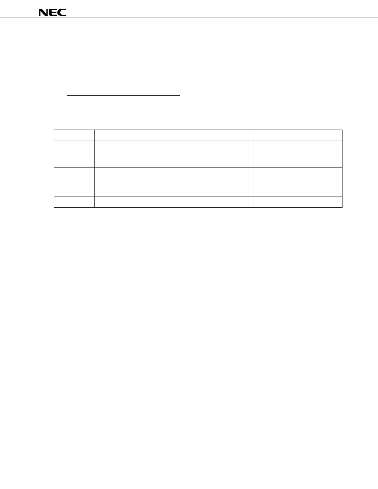
Functional Outline
*
µ
PD754144, 754244
Parameter
Instruction execution time • 4, 8, 16, 64 µs•0.95, 1.91, 3.81, 15.3 µs
(at fcc = 1.0-MHz operation) (at fx = 4.19-MHz operation)
On-chip Mask ROM 4096 × 8 bits (0000H-0FFFH)
memory RAM 128 × 4 bits (000H-07FH)
EEPROM 16 × 8 bits (400H-41FH)
System clock oscillator RC oscillator Crystal/ceramic oscillator
(External resistor and capacitor)
General-purpose register • 4-bit operation: 8 × 4 banks
• 8-bit operation: 4 × 4 banks
Input/output CMOS input 4 On-chip pull-up resistor can be specified by mask option.
port CMOS input/output 9 On-chip pull-up resistor connection can be specified by means of software.
Total 13
Start-up time after reset 56/fcc 217/fx, 215/fx (selected by mask option)
Stand-by mode release time 29/fcc 220/fx, 217/fx, 215/fx, 213/fx
Timer 4 channels
• 8-bit timer counter
(can be used as 16-bit timer counter) : 3 channels
• Basic interval/watchdog timer : 1 channel
Bit sequential buffer 16 bits
Vectored interrupt External: 1, Internal: 5
Test input External: 1 (key return reset function available)
Standby function STOP/HALT mode
Operating ambient temperature TA = –40 to +85 °C
Operating supply voltage VDD = 1.8 to 6.0 V
Package • 20-pin plastic SOP (300 mil, 1.27-mm pitch)
• 20-pin plastic shrink SOP (300 mil, 0.65-mm pitch)
µ
PD754144
µ
PD754244
• 0.67, 1.33, 2.67, 10.7 µs
(at fx = 6.0-MHz operation)
(selected by the setting of BTM)
Data Sheet U10040EJ2V1DS
3

µ
*
PD754144, 754244
CONTENTS
1. PIN CONFIGURATION (TOP VIEW) ....................................................................................................6
2. BLOCK DIAGRAM................................................................................................................................ 8
3. PIN FUNCTION .....................................................................................................................................9
3.1 Port Pins ...................................................................................................................................... 9
3.2 Non-port Pins ............................................................................................................................ 10
3.3 Pin Input/Output Circuits .........................................................................................................11
3.4 Recommended Connection of Unused Pins .......................................................................... 12
4. SWITCHING FUNCTION BETWEEN MK I MODE AND MK II MODE ............................................... 13
4.1 Difference between Mk I and Mk II Modes .............................................................................. 13
4.2 Setting Method of Stack Bank Select Register (SBS) ...........................................................14
5. MEMORY CONFIGURATION .............................................................................................................15
6. EEPROM .............................................................................................................................................18
7. PERIPHERAL HARDWARE FUNCTIONS .........................................................................................19
7.1 Digital Input/Output Ports ........................................................................................................ 19
7.2 Clock Generator ........................................................................................................................19
7.3 Basic Interval Timer/Watchdog Timer ..................................................................................... 22
7.4 Timer Counter ...........................................................................................................................23
7.5 Programmable Threshold Port (Analog Input Port) ............................................................... 27
7.6 Bit Sequential Buffer ....... 16 Bits ............................................................................................ 28
8. INTERRUPT FUNCTION AND TEST FUNCTION ..............................................................................29
9. STANDBY FUNCTION........................................................................................................................ 31
10. RESET FUNCTION .............................................................................................................................32
10.1 Configuration and Operation Status of RESET Function .....................................................32
10.2 Watchdog Flag (WDF), Key Return Flag (KRF) ......................................................................36
11. MASK OPTION ................................................................................................................................... 38
12. INSTRUCTION SETS .......................................................................................................................... 39
13. ELECTRICAL SPECIFICATIONS ......................................................................................................48
13.1µPD754144 .................................................................................................................................48
13.2µPD754244 .................................................................................................................................56
14. CHARACTERISTICS CURVES (REFERENCE VALUES) .................................................................67
14.1µPD754144 .................................................................................................................................67
14.2µPD754244 .................................................................................................................................69
4 Data Sheet U10040EJ2V1DS

µ
*
PD754144, 754244
15. RC OSCILLATION FREQUENCY CHARACTERISTICS EXAMPLES (REFERENCE VALUES) .....72
16. PACKAGE DRAWINGS ...................................................................................................................... 76
17. RECOMMENDED SOLDERING CONDITIONS .................................................................................. 78
APPENDIX A. COMPARISON OF FUNCTIONS AMONG µPD754144, 754244, AND 75F4264 ...........81
APPENDIX B. DEVELOPMENT TOOLS ................................................................................................. 82
APPENDIX C. RELATED DOCUMENTS ................................................................................................85
Data Sheet U10040EJ2V1DS
5
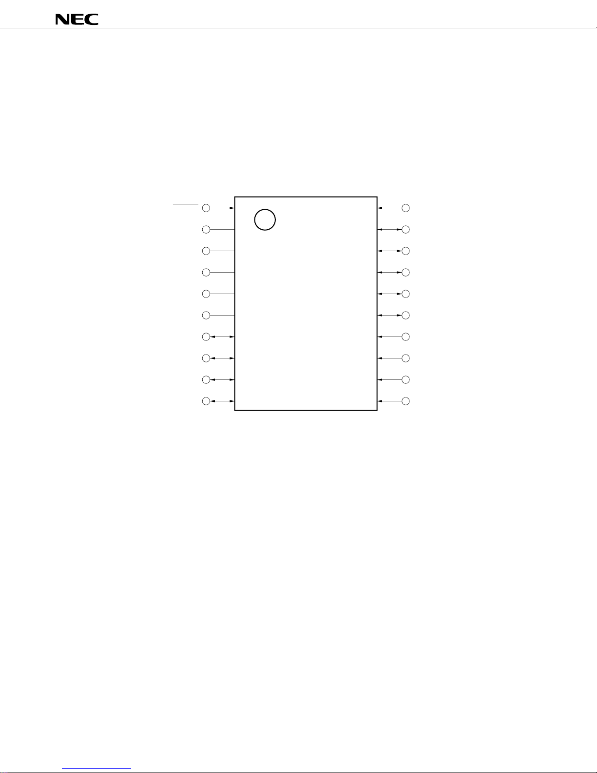
1. PIN CONFIGURATION (TOP VIEW)
*
•µPD754144
• 20-pin Plastic SOP (300 mil, 1.27-mm pitch)
µ
PD754144GS-×××-BA5
µ
★
★
PD754144GS-×××-BA5-A
• 20-pin Plastic Shrink SOP (300 mil, 0.65-mm pitch)
µ
PD754144GS-×××-GJG
µ
PD754144GS-×××-GJG-A
µ
PD754144, 754244
RESET
CL1
CL2
V
IC
V
P60/AVREF
P61/INT0
P62/PTH00
P63/PTH01
1
2
3
SS
DD
4
5
6
7
8
9
10
IC: Internally Connected (Connect to V
20
19
18
17
16
15
14
13
12
11
DD directly)
KRREN
P80
P30/PTO0
P31/PTO1
P32/PTO2
P33
P70/KR4
P71/KR5
P72/KR6
P73/KR7
6 Data Sheet U10040EJ2V1DS
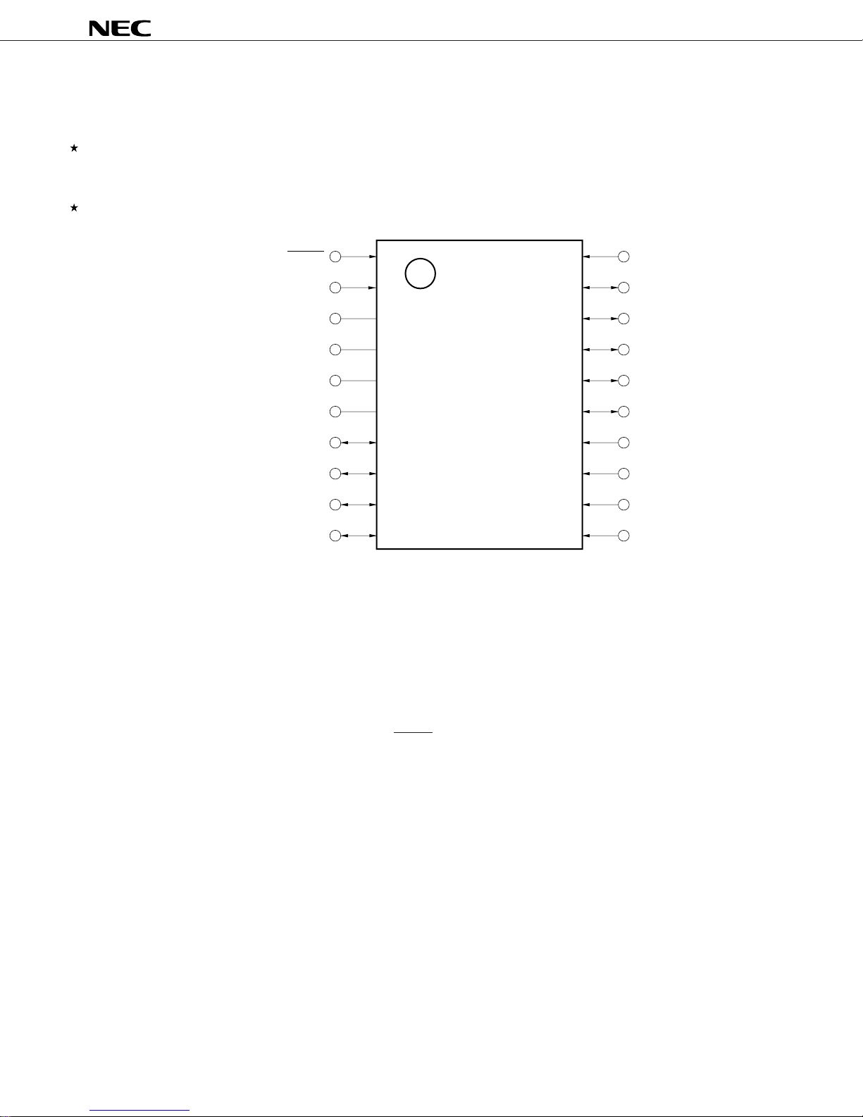
•µPD754244
*
• 20-pin Plastic SOP (300 mil, 1.27-mm pitch)
µ
PD754244GS-×××-BA5
µ
PD754244GS-×××-BA5-A
• 20-pin Plastic Shrink SOP (300 mil, 0.65-mm pitch)
µ
PD754244GS-×××-GJG
µ
PD754244GS-×××-GJG-A
µ
PD754144, 754244
RESET
X1
X2
V
IC
V
P60/AV
REF
P61/INT0
P62/PTH00
P63/PTH01
SS
DD
1
2
3
4
5
6
7
8
9
10
IC: Internally Connected (Connect to V
20
19
18
17
16
15
14
13
12
11
DD directly)
KRREN
P80
P30/PTO0
P31/PTO1
P32/PTO2
P33
P70/KR4
P71/KR5
P72/KR6
P73/KR7
Pin Identification
AVREF : Analog reference P70 to P73 : Port 7
CL1 and CL2 : System clock (RC) P80 : Port 8
IC : Internally connected PTH00 and PTH01 : Programmable threshold port analog inputs 0 and 1
INT0 : External vectored interrupt 0 PTO0 to PTO2 : Programmable timer outputs 0 to 2
KR4 to KR7 : Key returns 4 to 7 RESET : Reset
KRREN : Key return reset enable V
P30 to P33 : Port 3 V
P60 to P63 : Port 6 X1 and X2 : System clock (crystal/ceramic)
DD : Positive power supply
SS : Ground
Data Sheet U10040EJ2V1DS
7
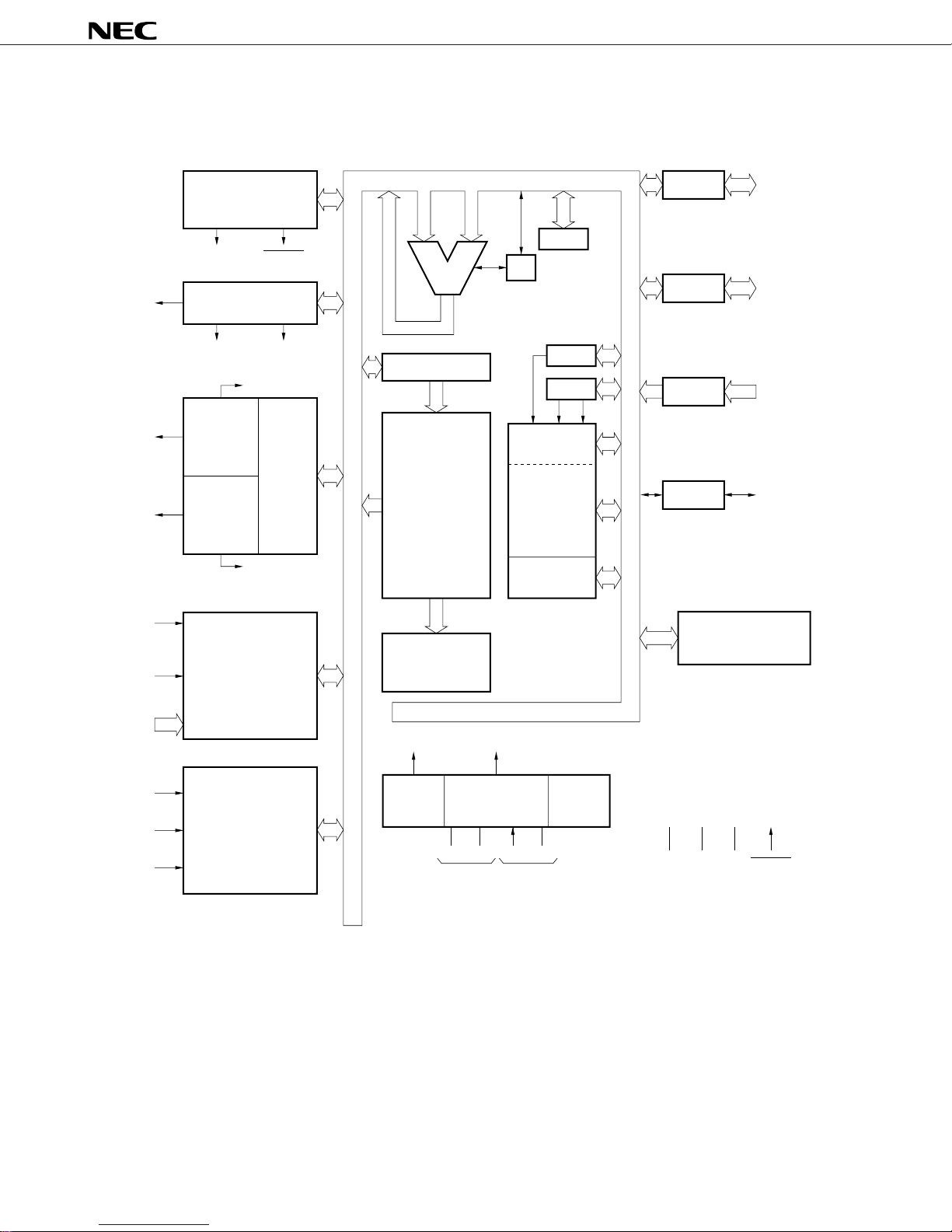
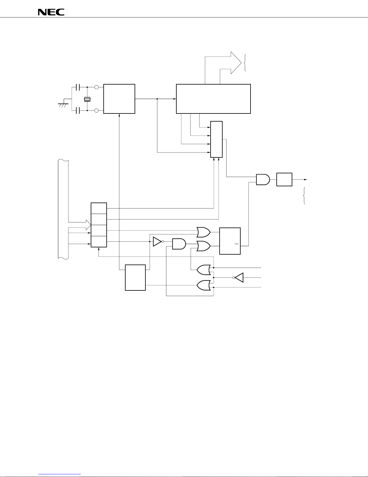
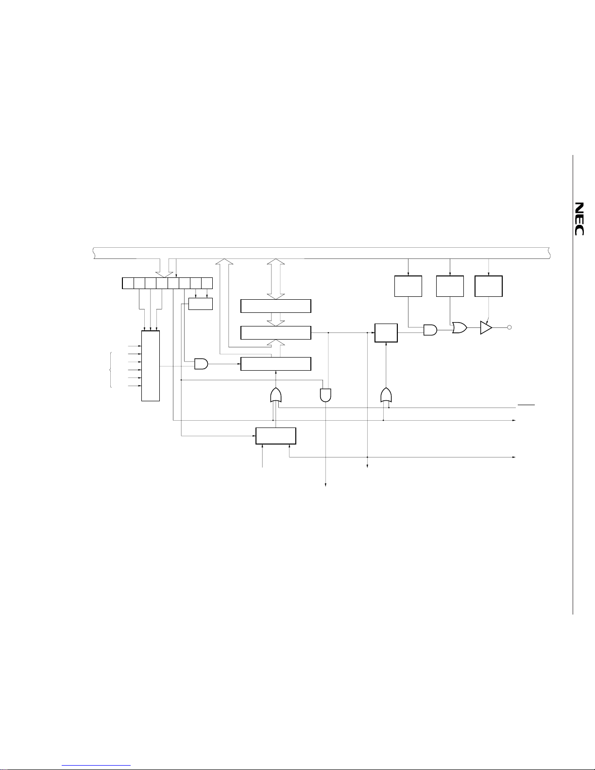
2. BLOCK DIAGRAM
*
µ
PD754144, 754244
PTO0/P30
PTO1/P31
PTO2/P32
INT0/P61
KRREN
BASIC INTERVAL
TIMER/WATCHDOG
TIMER
INTBT RESET
8-BIT TIMER
COUNTER#0
INTT0 TOUT
INTT1
8-BIT
TIMER
COUNTER#1
8-BIT
TIMER
COUNTER#2
CASCADED
16-BIT
TIMER
COUNTER
INTT2
INTERRUPT
CONTROL
ALU
PROGRAM COUNTER
PROGRAM MEMORY
(ROM)
4096
×
8 BITS
DECODE
AND
CONTROL
SP (8)
CY
SBS
BANK
GENERAL REG.
DATA MEMORY
(RAM)
128
×
4 BITS
EEPROM
16×8 BITS
PORT3 4
PORT6 4
PORT7 4
PORT8
BIT SEQ. BUFFER (16)
P30 to P33
P60 to P63
P70 to P73
P80
KR4/P70 to
KR7/P73
AV
REF
/P60
PTH00/P62
PTH01/P63
4
PROGRAMMABLE
THRESHOLD
PORT
fX/2
CLOCK
DIVIDER
N
SYSTEM CLOCK
GENERATOR
CL1 CL2 X1 X2
Apply to the
µPD754144
CPU CLOCK
Apply to the
µPD754244
φ
STAND BY
CONTROL
IC VDDVSSRESET
8 Data Sheet U10040EJ2V1DS

3. PIN FUNCTION
*
3.1 Port Pins
µ
PD754144, 754244
Pin Name Input/Output
P30 Input/Output PTO0 – Input E-B
P31 PTO1
P32 PTO2
P33 –
P60 Input/Output AV
P61 INT0
P62 PTH00
P63 PTH01
P70 Input KR4 – Input B -A
P71 KR5
P72 KR6
P73 KR7
P80 Input/Output – – Input F -A
Alternate
Function I/O TYPE
Programmable 4-bit input/output port
(PORT3).
This port can be specified input/output bitwise.
On-chip pull-up resistor connection can be
specified by software in 4-bit units.
REF – Input F -A
Programmable 4-bit input/output port (PORT6).
This port can be specified input/output bitwise.
On-chip pull-up resistor can be specified by
software in 4-bit units
Noise eliminator can be selected with P61/INT0.
4-bit input port (PORT7).
On-chip pull-up resistor can be specified by
software bit-wise.
1-bit input/output port (PORT8).
On-chip pull-up resistor connection can be
specified by software.
Function
Note2
.
8-bit
After Reset
I/O Circuit
Note 1
Notes 1. Circled characters indicate the Schmitt-trigger input.
2. Do not specify an on-chip pull-up resistor connection when using the programmable threshold port.
Data Sheet U10040EJ2V1DS
9

3.2 Non-port Pins
*
µ
PD754144, 754244
Pin Name Input/Output
PTO0 Output P30 Timer counter output pins Input E-B
PTO1 P31
PTO2 P32
INT0 Input P61 Edge detection vectored Noise elimination Input F -A
KR4 to KR7 Input P70 to P73 Falling edge detection testable input pins Input B -A
PTH00 Input P62 Threshold voltage-variable 2-bit analog input pins Input F -A
PTH01 P63
KRREN Input – Key return reset enable pin Input B
REF Input P60 Reference voltage input pin Input F -A
AV
CL1 ––Incorporated in the µPD754144 only ––
CL2 – External clock cannot be input.
Alternate
Function TYPE
interrupt input pin circuit can be
(detected edge can be selected.
selected) Asynchronous
Noise elimination circuit input
can be selected.
The reset signal is generated at the falling edge
of KRn while KRREN is high in STOP mode.
RC (for system clock oscillation) connection pin
Function
After Reset
I/O Circuit
Note
µ
X1 Input – Incorporated in the
Crystal/ceramic resonator (for system clock
oscillation) connection pin
X2 – When inputting the external clock, input the external
clock to pin X1 and input the inverted phase of the
external clock to pin X2.
RESET Input – System reset input pin (low-level active) – B -A
Pull-up resistor can be incorporated (mask option).
IC – – Internally Connected Connect directly to VDD.– –
VDD ––Positive supply pin – –
SS ––Ground potential – –
V
PD754244 only ––
Note Circled characters indicate the Schmitt-trigger input.
10 Data Sheet U10040EJ2V1DS
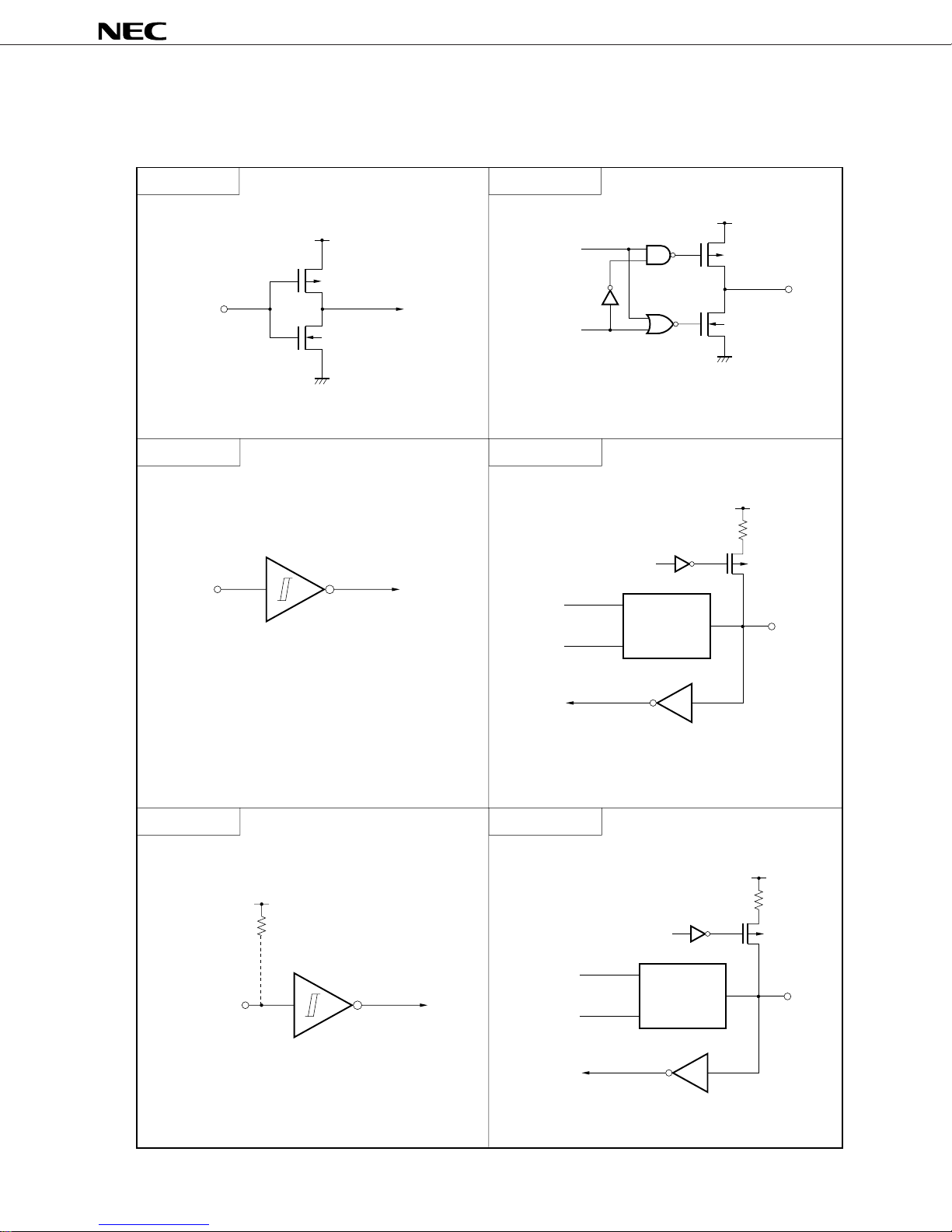
3.3 Pin Input/Output Circuits
*
The
µ
PD754244 pin input/output circuits are shown schematically.
µ
PD754144, 754244
TYPE A
IN
CMOS specification input buffer.
TYPE B
IN
TYPE D
V
DD
DD
V
P-ch
N-ch
data
output
disable
Push-pull output that can be placed in output
high-impedance (both P-ch, N-ch off).
TYPE E-B
P.U.R.
enable
data
Type D
output
disable
P-ch
N-ch
DD
V
OUT
P.U.R.
P-ch
IN/OUT
Schmitt-trigger input having hysteresis characteristic.
TYPE B-A
V
DD
P.U.R. (Mask Option)
IN
P.U.R. : Pull-Up Resistor
TYPE F-A
output
disable
data
Type A
P.U.R. : Pull-Up Resistor
P.U.R.
enable
Type D
Type B
P.U.R. : Pull-Up Resistor
V
DD
P.U.R.
P-ch
IN/OUT
Data Sheet U10040EJ2V1DS
11

3.4 Recommended Connection of Unused Pins
*
Table 3-1. List of Recommended Connection of Unused Pins
Pin Recommended Connecting Method
P30/PTO0 Input state : Independently connect to VSS or VDD via a resistor.
P31/PTO1 Output state: Leave open.
P32/PTO2
P33
P60/AVREF
P61/INT0
P62/PTH00
P63/PTH01
P70/KR4 Connect to VDD.
P71/KR5
µ
PD754144, 754244
P72/KR6
P73/KR7
P80 Input state : Independently connect to VSS or VDD via a resistor.
Output state: Leave open.
KRREN When this pin is connected to VDD, internal reset signal is gener-
ated at the falling edge of the KRn pin in the STOP mode.
When this pin is connected to VSS, internal reset signal is not
generated even if the falling edge of KRn pin is detected in the
STOP mode.
IC Connect directly to VDD.
12 Data Sheet U10040EJ2V1DS

4. SWITCHING FUNCTION BETWEEN MK I MODE AND MK II MODE
*
4.1 Difference between Mk I and Mk II Modes
The
µ
PD754244 75XL CPU has the following two modes: Mk I and Mk II, either of which can be selected. The
mode can be switched by the bit 3 of the Stack Bank Select register (SBS).
• Mk I mode: Instructions are compatible with the 75X series. Can be used in the 75XL CPU with a ROM
capacity of up to 16 Kbytes.
• Mk II mode: Incompatible with 75X series. Can be used in all the 75XL CPU’s including those products
whose ROM capacity is more than 16 Kbytes.
Table 4-1. Differences between Mk I Mode and Mk II Mode
Mk I Mode Mk II Mode
Number of stack bytes 2 bytes 3 bytes
for subroutine instructions
BRA !addr1 instruction Not available Available
CALLA !addr1 instruction
µ
PD754144, 754244
CALL !addr instruction 3 machine cycles 4 machine cycles
CALLF !faddr instruction 2 machine cycles 3 machine cycles
Caution The Mk II mode supports a program area exceeding 16 Kbytes for the 75X and 75XL Series.
Therefore, this mode is effective for enhancing software compatibility with products that
have a program area of more than 16 Kbytes.
With regard to the number of stack bytes during execution of subroutine call instructions,
the usable area increases by 1 byte per stack compared to the Mk I mode when the Mk II
mode is selected.
However, when the CALL !addr and CALLF !faddr instructions are used, the machine cycle
becomes longer by 1 machine cycle. Therefore, if more emphasis is placed on RAM use
efficiency and processing performance than on software compatibility, the Mk I mode
should be used.
Data Sheet U10040EJ2V1DS
13
µ
*
PD754144, 754244
4.2 Setting Method of Stack Bank Select Register (SBS)
Switching between the Mk I mode and Mk II mode can be done by the SBS. Figure 4-1 shows the format.
The SBS is set by a 4-bit memory manipulation instruction.
When using the Mk I mode, the SBS must be initialized to 1000B at the beginning of a program. When using
the Mk II mode, it must be initialized to 0000B.
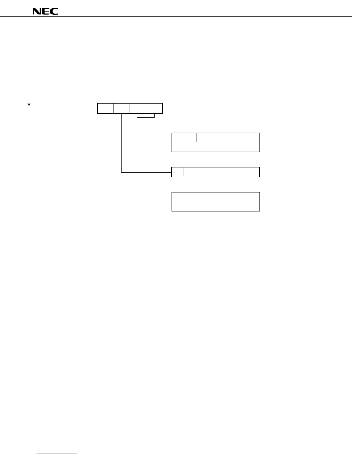
Figure 4-1. Stack Bank Select Register Format
Address
F84H SBS3 SBS2 SBS1 SBS0
32 10
Symbol
SBS
Stack area specification
0
Other than above setting prohibited
0
Mode switching specification
0
1
Memory bank 0
0
0 must be set in the bit 2 position
Mk II mode
Mk I mode
Caution Because SBS. 3 is set to “1” after a RESET signal is generated, the CPU operates in the
Mk I mode. When executing an instruction in the Mk II mode, set SBS. 3 to “0” to select
the Mk II mode.
14 Data Sheet U10040EJ2V1DS

µ
*
PD754144, 754244
5. MEMORY CONFIGURATION
• Program memory (ROM) • • • 4096 x 8 bits
• Addresses 0000H and 0001H
Vector table wherein the program start address and the values set for the RBE and MBE at the time a
RESET signal is generated are written. Reset and start are possible at an arbitrary address.
• Addresses 0002H to 000FH
Vector table wherein the program start address and values set for the RBE and MBE by the vectored
interrupts are written. Interrupt service can be started at an arbitrary address.
• Addresses 0020H to 007FH
Table area referenced by the GETI instruction
Note The GETI instruction realizes a 1-byte instruction on behalf of an arbitrary 2-byte instruction, 3-byte
instruction, or two 1-byte instructions. It is used to decrease the program steps.
• Data memory
• Data area
Static RAM
• • • 128 words x 4 bits (000H to 07FH)
EEPROM • • • 16 words x 8 bits (400H to 41FH)
• Peripheral hardware area
• • • 128 words x 4 bits (F80H to FFFH)
Note
.
Data Sheet U10040EJ2V1DS
15
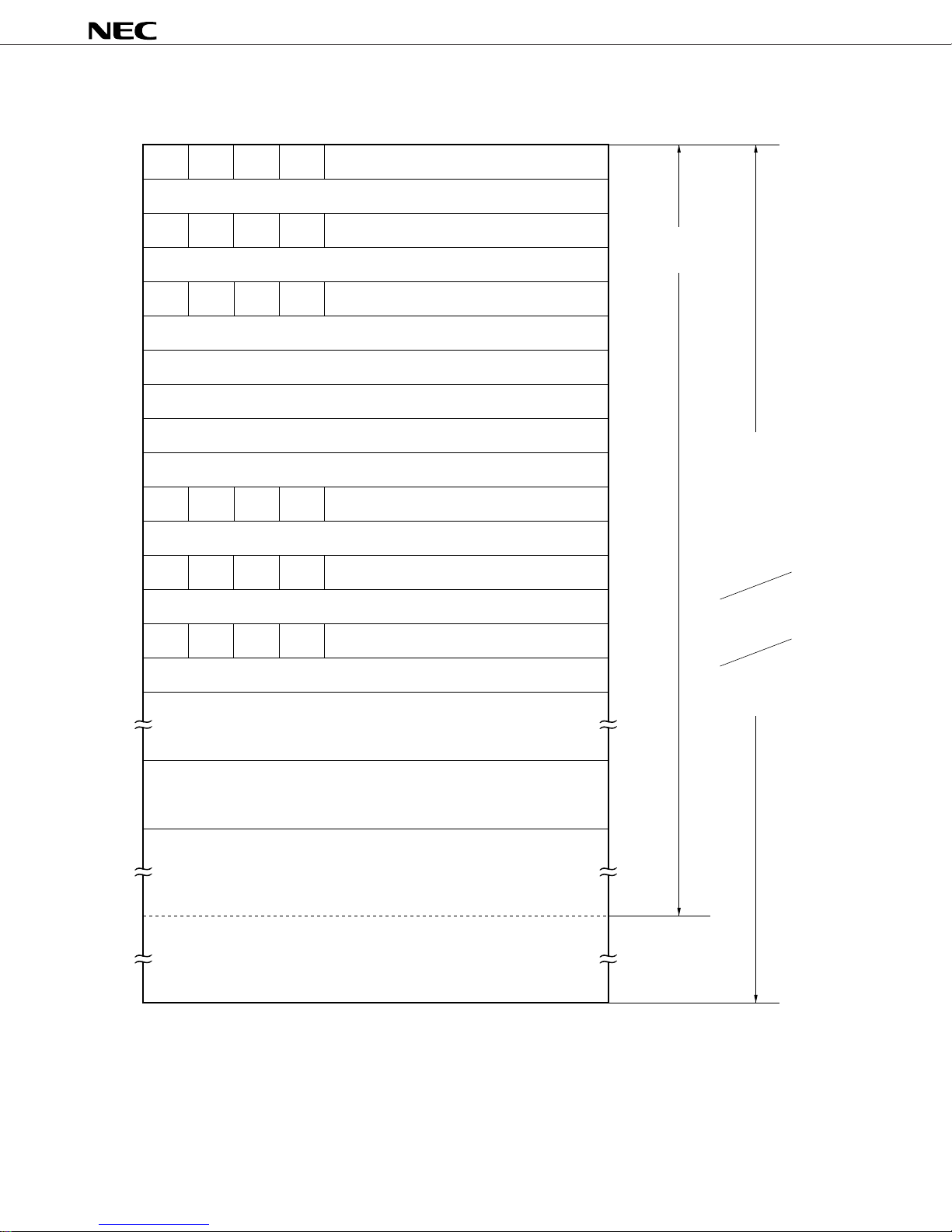
Figure 5-1. Program Memory Map
*
µ
PD754144, 754244
Address
0000H
0001H
0002H
0003H
0004H
0005H
0006H
0007H
0008H
0009H
000AH
000BH
000CH
7654 0
MBE RBE Internal reset start address (high-order 4 bits)
MBE RBE INTBT start address (high-order 4 bits)
MBE RBE INT0 start address (high-order 4 bits)
MBE RBE INTT0 start address (high-order 4 bits)
MBE RBE INTT1/INTT2 start address (high-order 4 bits)
0
0
Internal reset start address (low-order 8 bits)
0
0
INTBT start address (low-order 8 bits)
0
0
INT0 start address (low-order 8 bits)
0
0
INTT0 start address (low-order 8 bits)
0
0
CALLF !faddr instruction
entry address
Branch address of
BR !addr
BRCB !caddr
BR BCDE
BR BCXA
BRA !addr
CALL !addr
CALLA !addr
instructions
Note
Note
000DH
000EH
000FH
0020H
007FH
0080H
07FFH
0800H
0FFFH
MBE RBE
0
INTT1/INTT2 start address (low-order 8 bits)
0 INTEE start address (high-order 4 bits)
INTEE start address (low-order 8 bits)
GET instruction reference table
Note Can be used in the MkII mode only.
GETI Branch/call
Addresses
BR $addr instruction
relative branch address
(–15 to –1, +2 to +16)
Remark In addition to the above, a branch can be made to an address with the low-order 8-bits only of the
PC changed by means of a BR PCDE or BR PCXA instruction.
16 Data Sheet U10040EJ2V1DS
Data area
*
static RAM (128 × 4)
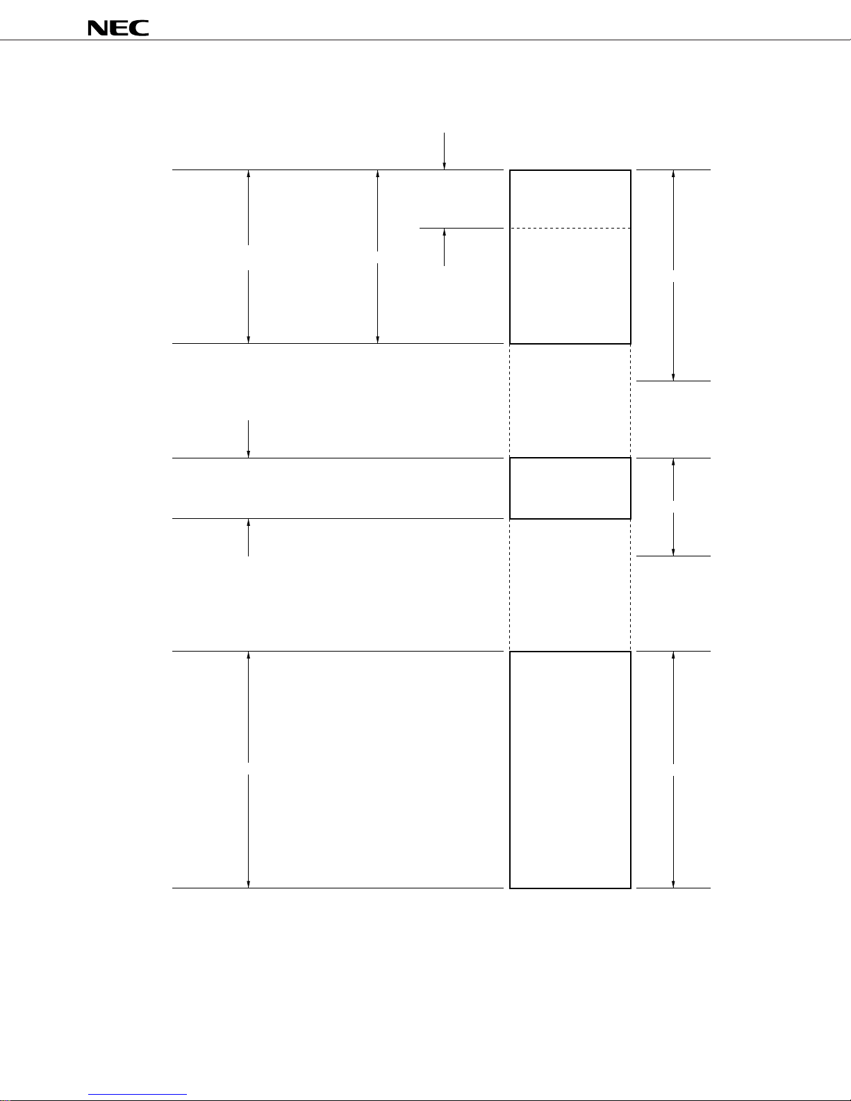
Figure 5-2. Data Memory Map
000H
General-purpose
register area
01FH
020H
Stack area
07FH
080H
µ
PD754144, 754244
Data memory Memory bank
(32 × 4)
128 × 4
(96 × 4)
0
Data area
EEPROM (16 × 8)
Peripheral hardware area
0FFH
400H
41FH
420H
4FFH
F80H
Not incorporated
16 × 8
Not incorporated
128 × 4
4
15
FFFH
Data Sheet U10040EJ2V1DS
17

µ
*
PD754144, 754244
6. EEPROM
The µPD754244 incorporates 16 words × 8 bit EEPROM (Electrically Erasable PROM) as well as static RAM
(128 words × 4 bit) as a data memory.
The EEPROM incorporated into the
(1) Written data is retained if power is turned off.
(2) 8-bit data manipulation (auto-erase/auto-write) is available by memory manipulation instruction as well as
for static RAM. However available instructions are restricted.
(3) It can reduce loads of software because the auto-erase and/or auto-write operation is performed by
hardware.
(4) Write operation control using the interrupt request
The interrupt request is generated under following conditions.
• Terminates write operation
•Write status flag
It is possible to check whether enables or disables write operation by bit manipulation instructions.
µ
PD754244 has the following features.
18 Data Sheet U10040EJ2V1DS
µ
*
PD754144, 754244
7. PERIPHERAL HARDWARE FUNCTIONS
7.1 Digital Input/Output Ports
The following two types of I/O ports are provided.
• CMOS input (Port 7) : 4
• CMOS I/O (Ports 3, 6, 8) : 9
Total : 13
Table 7-1. Types and Features of Digital Ports
Port Name Function Operation and Features Remarks
PORT3 4-bit I/O Can be set to input or output mode bit-wise. Also used as PTO0 to PTO2 pins.
PORT6 Also used as AV
and PTH01 pins.
PORT7 4-bit input 4-bit input only port Also used as KR4 to KR7 pins.
On-chip pull-up resistor connection can be specified
by mask option bit-wise.
PORT8 1-bit I/O Can be set to input or output mode bit wise. _
REF, INT0, PTH00,
7.2 Clock Generator
The clock generator provides the clock signals to the CPU and peripheral hardware. Its configuration is shown
in Figures 7-1 and 7-2.
The operation of the clock generator is set with the processor clock control register (PCC).
The instruction execution time can be changed.
•
µ
PD754144
• 4, 8, 16, 64 µs (when the system clock f
•
µ
PD754244
CC operates at 1.0 MHz)
• 0.95, 1.91, 3.81, 15.3 µs (when the system clock fX operates at 4.19 MHz)
• 0.67, 1.33, 2.67, 10.7 µs (when the system clock f
X operates at 6.0 MHz)
Data Sheet U10040EJ2V1DS
19

Figure 7-1. µPD754144 (RC Oscillation) Clock Generator Block Diagram
*
· Basic interval timer (BT)
· Timer counter
· INT0 noise eliminator
CL1
1/1~1/4096
Divider
CL2
System
clock
oscillator
cc
f
1/2 1/4 1/16
µ
PD754144, 754244
Oscillation stops
PCC
PCC0
Internal bus
HALT
STOP
PCC1
4
PCC2
Note
PCC3
Note
PCC2,
PCC3
clear
Note Instruction execution
STOP F/F
S
Q
R
Selector
Divider
1/4 Φ
· CPU
· INT0 noise
eliminator
HALT F/F
S
RQ
Wait release signal from BT
Reset signal
Standby release signal from
interrupt control circuit
Remarks 1. f
cc: System clock frequency
2. Φ = CPU clock
3. PCC: Processor Clock Control Register
4. One clock cycle (t
CY) of the CPU clock is equal to one machine cycle of the instruction.
20 Data Sheet U10040EJ2V1DS
µ
*
PD754144, 754244
Figure 7-2. µPD754244 (Crystal/Ceramic Oscillation) Clock Generator Block Diagram
· Basic interval timer (BT)
· Timer counter
· INT0 noise eliminator
X1
1/1~1/4096
Divider
X2
System
clock
oscillator
X
f
1/2 1/4 1/16
PCC
PCC0
Internal bus
HALT
STOP
PCC1
4
PCC2
Note
PCC3
Note
PCC2,
PCC3
clear
Note Instruction execution
Oscillation stops
STOP F/F
S
Q
R
Selector
Divider
1/4 Φ
· CPU
· INT0 noise
eliminator
HALT F/F
S
RQ
Wait release signal from BT
Reset signal
Standby release signal from
interrupt control circuit
Remarks 1. f
X: System clock frequency
2. Φ = CPU clock
3. PCC: Processor Clock Control Register
4. One clock cycle (t
CY) of the CPU clock is equal to one machine cycle of the instruction.
Data Sheet U10040EJ2V1DS
21

7.3 Basic Interval Timer/Watchdog Timer
*
The basic interval timer/watchdog timer has the following functions.
(a) Interval timer operation to generate a reference time interrupt
(b) Watchdog timer operation to detect a runaway of program and reset the CPU
(c) Selects and counts the wait time when the standby mode is released (
(d) Reads the contents of counting
Figure 7-3. Basic Interval Timer/Watchdog Timer Block Diagram
From clock
generator
f
fX/2
fX/2
fX/2
5
X
/2
7
MPX
9
12
Basic interval timer
(8-bit frequency divider)
Clear
BT
µ
PD754144, 754244
µ
PD754244 only)
Set
Note 1
Clear
BT
interrupt
request flag
IRQBT
Vectored
interrupt
request signal
BTM3 BTM2 BTM1 BTM0 BTM
SET1
Note 2
4
Notes 1. In the
is released. The oscillation stabilization wait time is negligible in the
returns to the normal operation mode after counting 2
In the µPD754244 (crystal/ceramic oscillation), on the other hand, the wait time can be specified
when the standby mode is released.
2. Instruction execution.
3
81
Internal bus
µ
PD754144 (RC oscillation), the wait time cannot be specified when the standby mode
Wait release signal
when standby is
released
Note 1
.
9
/fCC (512 µs: @ fCC = 1.0-MHz operation).
WDTM
Note 2
SET1
µ
PD754144 and this device
Internal reset
signal
22 Data Sheet U10040EJ2V1DS
7.4 Timer Counter
*
The
µ
PD754244 incorporates three channels of timer counters. Its configuration is shown in Figures 7-4 to
7-6.
The timer counter has the following functions.
(a) Programmable interval timer operation
(b) Square wave output of any frequency to PTO0-PTO2 pins
(c) Count value read function
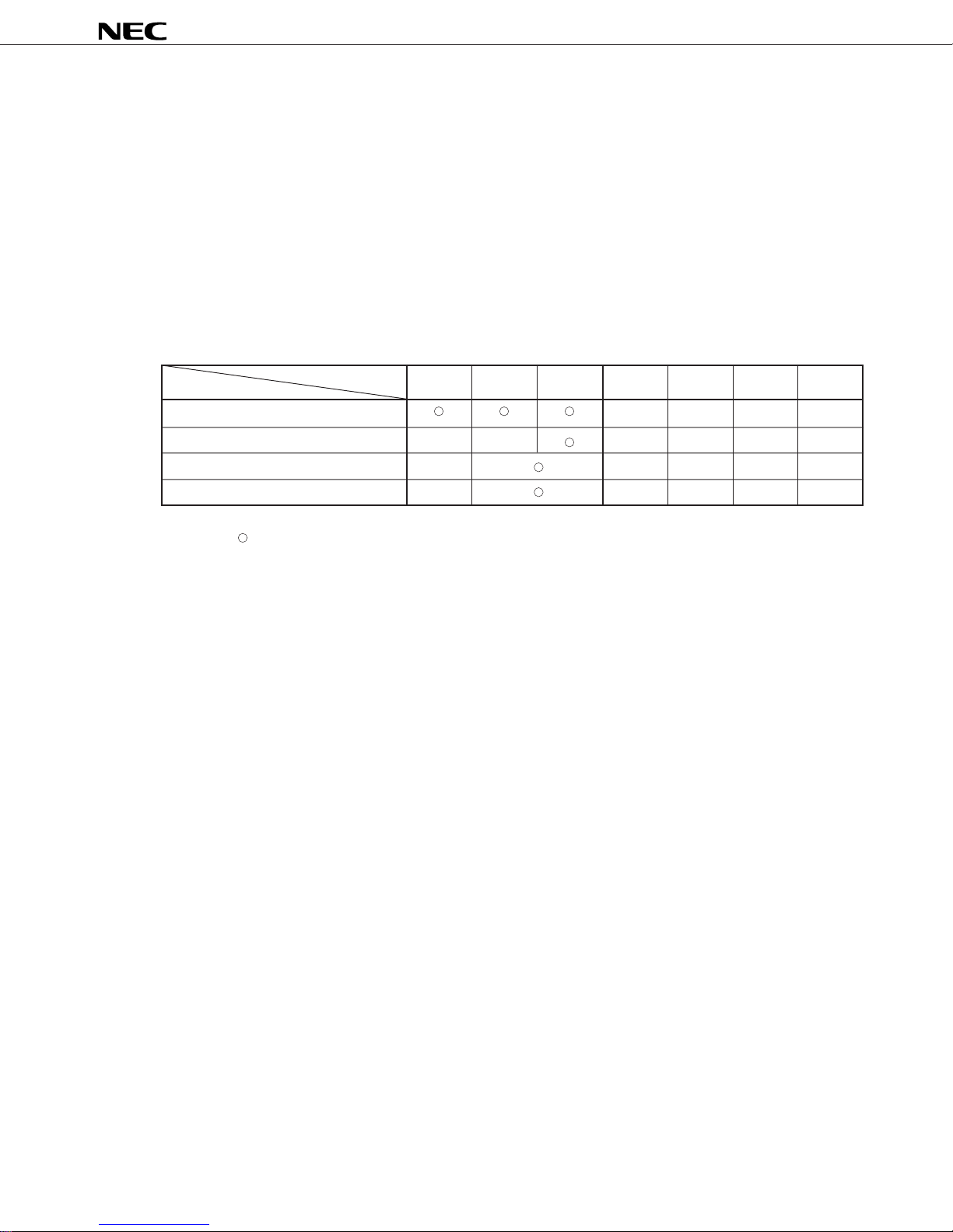
The timer counter can operate in the following four modes as set by the mode register.
Table 7-2. Mode List
µ
PD754144, 754244
Mode
8-bit timer counter mode
PWM pulse generator mode ××
16-bit timer counter mode ×
Carrier generator mode ×
Channel
Channel 0 Channel 1 Channel 2
Remark :Available
× : Not available
TM11 TM10 TM21 TM20
0000
0001
1010
0011
Data Sheet U10040EJ2V1DS
23
µ
PD754144, 754244
24 Data Sheet U10040EJ2V1DS
Figure 7-4. Timer Counter (Channel 0) Block Diagram
Note Instruction execution
Caution When setting data to TM0, be sure to set bits 0 and 1 to 0.
– TM06
f
x
/2
4
fx/2
6
fx/2
8
fx/2
10
TM05 TM04 TM03 TM02 0 0
TM0
Match
SET1
Note
888
MPX
From clock
generator
Timer operation start
CP
Clear
Count register (8)
T0
8
8
Comparator (8)
Modulo register (8)
TMOD0
TOUT
F/F
Reset
TOE0 PORT3.0 PMGA bit 0
T0
enable flag
P30
Output latch
Port 3
input/output
mode
Output buffer
P30/PTO0
INTT0
IRQT0
set signal
RESET
IRQT0
clear signal
Internal bus
*
µ
PD754144, 754244
25
Data Sheet U10040EJ2V1DS
8
8
8
8
TM15 TM14 TM13 TM12 TM11 TM10TM16–
TM1
Decoder
MPX
Timer counter (channel 2) output
From clock
generator
CP
Clear
T1
Count register (8)
Comparator (8)
Modulo register (8)
TMOD1
SET
Note
Timer operation start
16 bit timer counter mode
Selector
Match
Reset
TOUT
F/F
TOE1 PORT3.1 PMGA bit 1
T1
enable flag
P31
Output latch
Port 3
input/output
mode
Output buffer
P31/PTO1
INTT1
IRQT1
set signal
RESET
IRQT1
clear signal
Timer counter (channel 2) match signal
(When 16-bit timer counter mode)
Timer counter (channel 2) comparator
(When 16-bit timer counter mode)
Timer counter (channel 2) reload signal
Internal bus
f
x
/2
5
fx/2
6
fx/2
8
fx/2
10
fx/2
12
Figure 7-5. Timer Counter (Channel 1) Block Diagram
Note Instruction execution
*

µ
PD754144, 754244
26 Data Sheet U10040EJ2V1DS
Figure 7-6. Timer Counter (Channel 2) Block Diagram
Note Instruction execution
Caution When setting data to TC2, be sure to set bit 7 to 0.
Internal bus
888
88
8
8
TM25 TM24 TM23 TM22 TM21 TM20TM26
–
MPX
Decoder
From clock
generator
CP
16-bit timer counter mode
Timer operation start
Count register (8)
Comparator (8)
MPX (8)
Match
TOUT
F/F
T2
High-level period
setting modulo register (8)
Modulo register (8)
Reset
––
TOE2 REMC NRZB
NRZ–
0
8
TMOD2TMODH TC2
Reload
Overflow
Carrier generator mode
PORT3.2 PMGA bit 2
Output
latch
Port 3
input/output
mode
Output buffer
P32/PTO2
Timer counter (channel 1)
clock input
INTT2
IRQT2
set signal
RESET
IRQT2 clear signal
Timer counter (channel 1) match signal
(When 16-bit timer counter mode)
Timer counter (channel 1) clear
signal (When 16-bit timer mode)
Timer counter (channel 1) match signal
(When Carrier generator mode)
TM2
Clear
Selector
Selector
SET
Note
f
x
fx/2
f
x
/2
4
fx/2
6
fx/2
8
fx/2
10
*
µ
*
PD754144, 754244
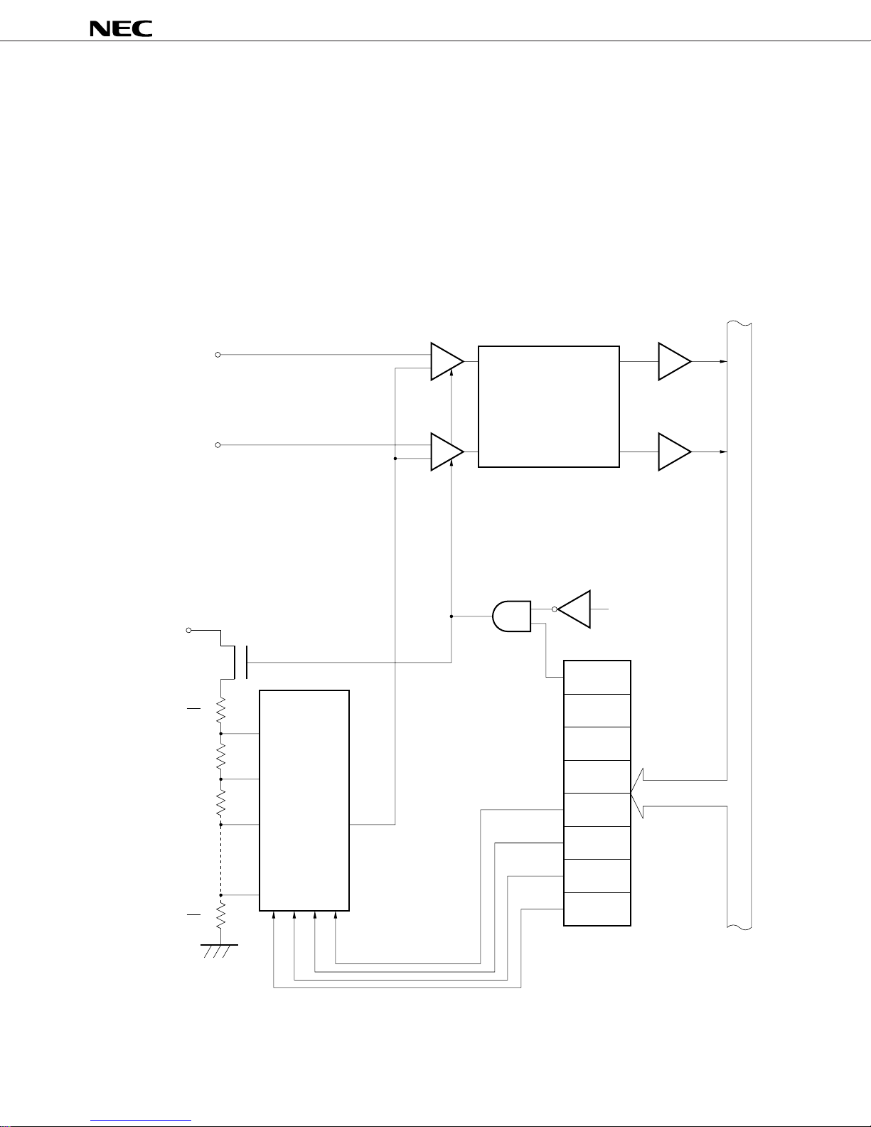
7.5 Programmable Threshold Port (Analog Input Port)
The
µ
PD754244 provides analog input pins (PTH00, PTH01) whose threshold voltage (reference voltage) is
selectable within sixteen steps. The following operations can be performed with these analog input pins.
(1) Comparator operation
(2) 4-bit resolution A/D converter operation (controlled by software)
Caution Do not specify an on-chip pull-up resistor connection for Port 6 when using the programmable
threshold port.
Figure 7-7. Programmable Threshold Port Block Diagram
PTH00
PTH01
REF
AV
1
2
PTH0
+
–
Programmable
threshold
port input latch (2)
+
–
Operate/stop
R
R
R
MPX
REF
V
Standby mode signal
PTHM7
PTHM6
PTHM5
PTHM4
PTHM3
PTHM2
Input buffer
Input buffer
Internal bus
8
1
R
2
Data Sheet U10040EJ2V1DS
PTHM1
PTHM0
PTHM
27

µ
*
PD754144, 754244
7.6 Bit Sequential Buffer ....... 16 Bits
The bit sequential buffer (BSB) is a special data memory for bit manipulation and the bit manipulation can be
easily performed by changing the address specification and bit specification in sequence, therefore it is useful
when processing large data bit-wise.
Figure 7-8. Bit Sequential Buffer Format
Address
Bit
Symbol
L register L = FH
FC3H FC2H FC1H FC0H
3210321032 10 32 10
BSB3 BSB2 BSB1 BSB0
L = CH L = BH L = 8H L = 7H L = 4H L = 3H
DECS L
INCS L
L = 0H
Remarks 1. In the pmem.@L addressing, the specified bit moves corresponding to the L register.
2. In the pmem.@L addressing, the BSB can be manipulated regardless of MBE/MSB specification.
28 Data Sheet U10040EJ2V1DS

µ
*
PD754144, 754244
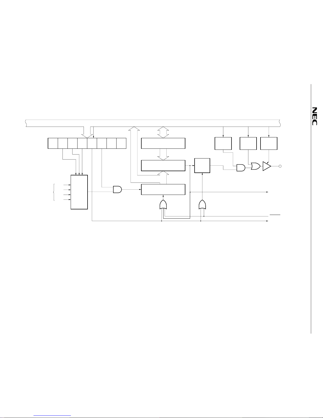
8. INTERRUPT FUNCTION AND TEST FUNCTION
Figure 8-1 shows the interrupt control circuit. Each hardware device is mapped in the data memory
space.
The interrupt control circuit of the
(1) Interrupt function
• Vectored interrupt function for hardware control, enabling/disabling the interrupt acknowledgement by
the interrupt enable flag (IE×××) and interrupt master enable flag (IME).
• Can set any interrupt start address.
• Multiple interrupts wherein the order of priority can be specified by the interrupt priority select register
(IPS).
• Test function of interrupt request flag (IRQ×××). An interrupt generated can be checked by software.
• Release the standby mode. A release interrupt can be selected by the interrupt enable flag.
(2) Test function
• Test request flag (IRQ2) generation can be checked by software.
• Release the standby mode. The test source to be released can be selected by the test enable flag.
µ
PD754244 has the following functions.
Data Sheet U10040EJ2V1DS
29

µ
PD754144, 754244
30 Data Sheet U10040EJ2V1DS
Figure 8-1. Interrupt Control Circuit Block Diagram
Notes 1. Noise eliminator (Standby release is disable when noise eliminator is selected.)
2. The INT2 pin is not provided. Interrupt request flag (IRQ2) is set at the KRn pin falling edge when IM20 = 1 and IM21 = 0.
Internal bus
Interrupt enable flag (IE×××)
24
IM2 IM0
Note1
Edge
detector
INT0/P61
INTBT
INTT0
INTT1
INTT2
INTEE
IRQBT
IRQ0
IRQT0
IRQT1
IRQT2
IRQEE
IRQ2
KR4/P70
KR7/P73
Falling edge
detector
Note2
Key return reset circuit
IM2
IME IPS IST1 IST0
Decoder
VRQn
Priority control
ciricuit
Standby release
signal
Selector
Vector table
address
generator
*
µ
*
PD754144, 754244
9. STANDBY FUNCTION
In order to reduce power dissipation while a program is in a standby mode, two types of standby modes (STOP
mode and HALT mode) are provided for the
Table 9-1. Operation Status in Standby Mode
µ
PD754244.
Item
Set instruction STOP instruction HALT instruction
Operation Clock generator Operation stops. Only the CPU clock Φ halts (oscillation
status continues).
Basic interval timer/ Operation stops. Operable
watchdog timer BT mode: The IRQBT is set in the basic
Timer Operation stops. Operable.
External interrupt INT0 is not operable.
CPU The operation stops.
Release signal
Mode
INT2 is operable during KRn falling period only.
•Reset signal • Reset signal
• Interrupt request signal sent from • Interrupt request signal sent from
interrupt enabled peripheral hardware interrupt enabled peripheral hardware
• System reset signal (key return reset)
generated by KRn falling edge when the
KRREN pin = 1
STOP Mode HALT Mode
time interval.
WT mode: Reset is generated by the
BT overflow.
Note
Note Can operate only when the noise eliminator is not used (IM02 = 1) by bit 2 of the edge detection mode
register (IM0).
Data Sheet U10040EJ2V1DS
31
µ
*
PD754144, 754244
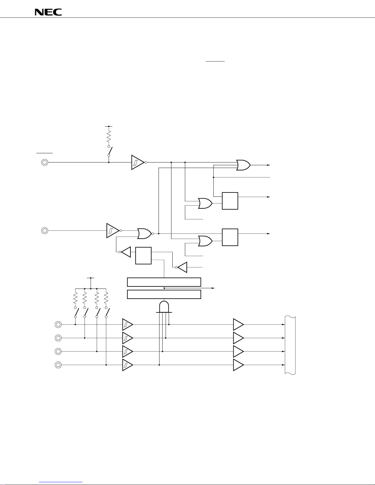
10. RESET FUNCTION
10.1 Configuration and Operation Status of RESET Function
There are three kinds of reset input: the external reset signal (RESET), the reset signal sent from the basic
interval/watchdog timer, and the reset signal generated by a falling edge signal from KRn in the STOP mode. When
any of these reset signals is input, an internal reset signal is generated. The configuration is shown in Figure
10-1.
Figure 10-1. Configuration of Reset Function
V
DD
Mask option
RESET
Output buffer
Internal reset signal
Watchdog timer overflow
KRREN
Mask option
P70/KR4
P71/KR5
P72/KR6
P73/KR7
QS
R
Instruction
QS
R
QR
S
V
DD
One-shot pulse generator
Falling edge detector
Instruction
STOP mode
Interrupt
WDF
KRF
Internal bus
32 Data Sheet U10040EJ2V1DS

µ
p
*
PD754144, 754244
Each hardware is initialized by the RESET signal generation as listed in Table 10-1. Figure 10-2 shows the
timing chart of the reset operation.
Figure 10-2. Reset Operation by RESET Signal Generation
Note
Wait
RESET
signal
generated
Operation mode or
standby mode
Operation modeHALT mode
Note In the
In the
the mask option.
Internal reset o
µ
PD754144, the wait time is fixed to 56/fcc (56µs: @ 1.0-MHz operation).
µ
PD754244, the wait time can be selected from the following two time settings by means of
17
2
/fx (21.8 ms : @ 6.0-MHz operation, 31.3 ms: @ 4.19-MHz operation)
15
2
/fx (5.46 ms : @ 6.0-MHz operation, 7.81 ms: @ 4.19-MHz operation)
eration
Data Sheet U10040EJ2V1DS
33

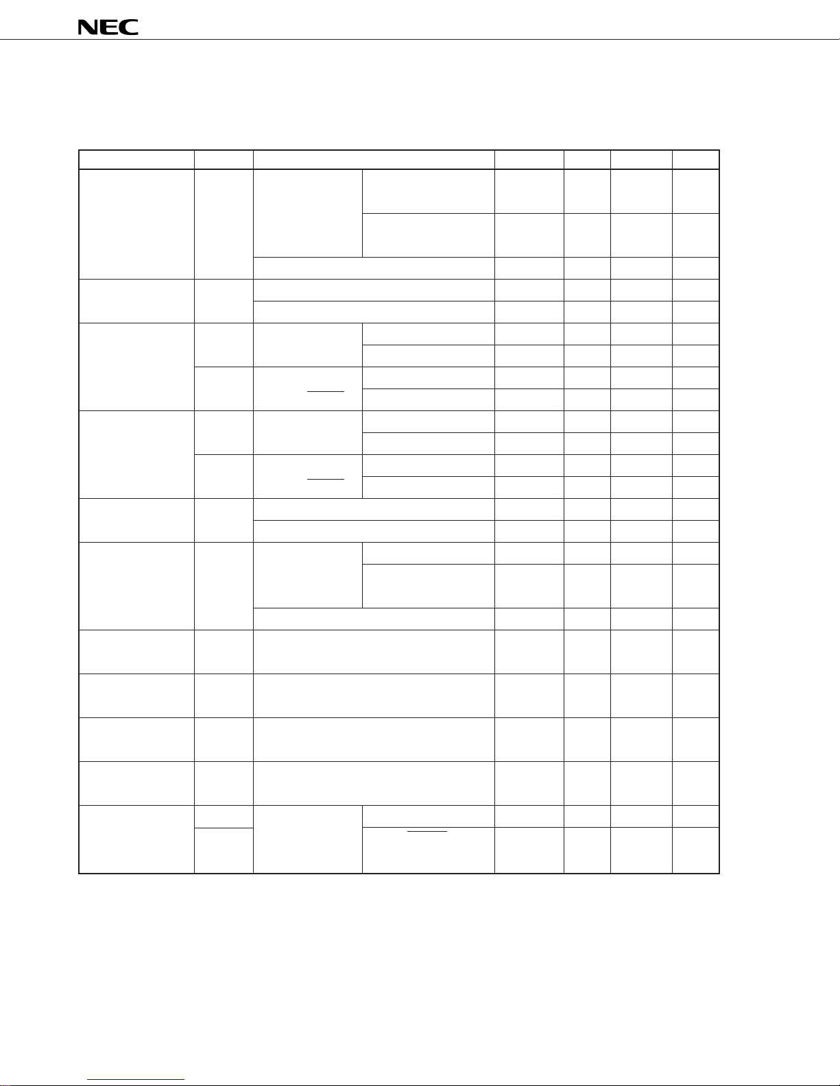
Table 10-1. Hardware Status After Reset (1/3)
*
µ
PD754144, 754244
Hardware
Program counter (PC) Sets the low-order 4 bits of Sets the low-order 4 bits of
PSW Carry flag (CY) Held Undefined
Skip flag (SK0 to SK2) 0 0
Interrupt status flag (IST0, IST1) 0 0
Bank enable flag (MBE, RBE) Sets the bit 6 of program Sets the bit 6 of program
Stack pointer (SP) Undefined Undefined
Stack bank select register (SBS) 1000B 1000B
Data memory (RAM) Held Undefined
Data memory (EEPROM) Held
EEPROM write control register (EWC) 0 0
General-purpose register (X, A, H, L, D, E, B, C) Held Undefined
Bank select register (MBS, RBS) 0, 0 0, 0
Basic interval
timer/watchdog
timer
Timer counter Counter (T0) 0 0
(channel 0) Modulo register (TMOD0) FFH FFH
Timer counter Counter (T1) 0 0
(channel 1) Modulo register (TMOD1) FFH FFH
Timer counter Counter (T2) 0 0
(channel 2) Modulo register (TMOD2) FFH FFH
Counter (BT) Undefined Undefined
Mode register (BTM) 0 0
Watchdog timer enable flag (WDTM)
Mode register (TM0) 0 0
TOE0, TOUT F/F 0, 0 0, 0
Mode register (TM1) 0 0
TOE1, TOUT F/F 0, 0 0, 0
High-level period setting modulo FFH FFH
register (TMOD2H)
Mode register (TM2) 0 0
TOE2, TOUT F/F 0, 0 0, 0
REMC, NRZ, NRZB 0, 0, 0 0, 0, 0
RESET signal generation RESET signal generation
in the standby mode in operation
program memory’s address program memory’s address
0000H to the PC11-PC8 and the 0000H to the PC11-PC8 and the
contents of address 0001H to contents of address 0001H to
the PC7-PC0. the PC7-PC0.
memory’s address 0000H to memory’s address 0000H to
the RBE and bit 7 to the MBE. the RBE and bit 7 to the MBE.
Note 1
00
Held
Note 2
Notes 1. Undefined if STOP mode is entered during an EEPROM write operation. Also undefined if HALT mode
is entered during a write operation and a RESET signal is input during a write operation.
2. If a RESET signal is input during an EEPROM write operation, the data at that address is undefined.
34 Data Sheet U10040EJ2V1DS

Table 10-1. Hardware Status After Reset (2/3)
*
µ
PD754144, 754244
Hardware
Programmable threshold port mode register (PTHM) 00H 00H
Clock generator
Interrupt Interrupt request flag (IRQ×××) Reset (0) Reset (0)
function Interrupt enable flag (IE×××)0 0
Digital port Output buffer Off Off
Bit sequential buffer (BSB0-BSB3) Held Undefined
Processor clock control register (PCC) 0 0
Interrupt priority selection register (IPS)
INT0, 2 mode registers (IM0, IM2) 0, 0 0, 0
Output latch Cleared (0) Cleared (0)
I/O mode registers (PMGA, C) 0 0
Pull-up resistor setting register (POGA, B)
RESET signal generation RESET signal generation
in the standby mode in operation
00
00
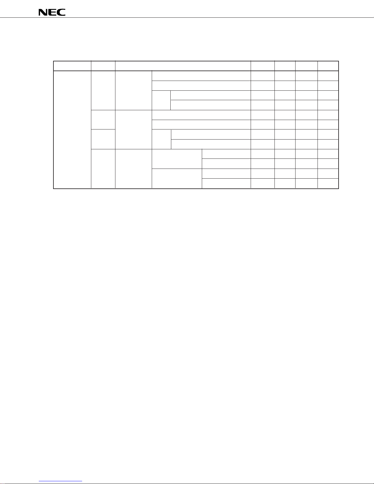
Table 10-1. Hardware Status After Reset (3/3)
RESET signal RESET signal RESET signal RESET signal
Hardware generation by key generation in the generation by WDT generation during
return reset standby mode during operation operation
Watchdog flag (WDF)
Hold the previous status
010
Key return flag (KRF) 1 0
Hold the previous status
0
Data Sheet U10040EJ2V1DS
35
µ
p
*
PD754144, 754244
10.2 Watchdog Flag (WDF), Key Return Flag (KRF)
The WDF is cleared by a watchdog timer overflow signal, and the KRF is set by a reset signal generated by
the KRn pins. As a result, by checking the contents of WDF and KRF, it is possible to know what kind of reset
signal is generated.
As the WDF and KRF are cleared only by external signal or instruction execution, if once these flags are set,
they are not cleared until an external signal is generated or a clear instruction is executed. Check and clear the
contents of WDF and KRF after reset start operation by executing SKTCLR instruction and so on.
Table 10-2 lists the contents of WDF and KRF corresponding to each signal. Figure 10-3 shows the WDF
operation in generating each signal, and Figure 10-4 shows the KRF operation in generating each signal.
Table 10-2. WDF and KRF Contents Correspond to Each Signal
External RESET
Hardware signal generation
Watchdog flag (WDF) 0 1 Hold 0 Hold
Key return flag (KRF) 0 Hold 1 Hold 0
Reset signal
generation by watch-
dog timer overflow
generation by the instruction instruction
Reset signal WDF clear KRF clear
KRn input execution execution
Figure 10-3. WDF Operation in Generating Each Signal
WDF clear
instruction
execution
WDF
External RESET
Operation mode
Operation mode
Reset signal generation by
watchdog timer overflow
HALT
mode
External RESET
signal generation
Operation
mode
Reset signal generation by
watchdog timer overflow
HALT
mode
Operation
mode
HALT
mode
Operation mode
Internal reset o
36 Data Sheet U10040EJ2V1DS
eration Internal reset operation Internal reset operation
µ
p
*
PD754144, 754244
Figure 10-4. KRF Operation in Generating Each Signal
KRF
External RESET
Operation mode
Operation mode
Reset signal
generation by
the KRn input
STOP instruction
execution
STOP
mode
HALT
mode
Internal reset o
Operation
External RESET
signal generation
mode
eration
Reset signal
generation by
the KRn input
STOP instruction
execution
HALT
mode
Internal reset operation Internal reset operation
Operation
mode
STOP
mode
KRF clear instruction
execution
HALT
mode
Operation mode
Data Sheet U10040EJ2V1DS
37

11. MASK OPTION
*
The µPD754244 has the following mask options:
• Mask option of P70/KR4 to P73/KR7
On-chip pull-up resistor connection can be specified for these pins.
(1) Do not connect an on-chip pull-up resistor
(2) Connect the 100-kΩ (typ.) pull-up resistor bit-wise
• Mask option of RESET pin
On-chip pull-up resistor connection can be specified for this pin.
(1) Do not connect an on-chip pull-up resistor
(2) Connect the 100-kΩ (typ.) pull-up resistor
µ
PD754144, 754244
• Standby function mask option (µPD754244 only)
The wait time when the RESET signal is input can be selected.
(1) 217/fX (21.8 ms: @ fX = 6.0-MHz operation, 31.3 ms: @ fX = 4.19-MHz operation)
15
(2) 2
/fX (5.46 ms: @ fX = 6.0-MHz operation, 7.81 ms: @ fX = 4.19-MHz operation)
Note This mask option is not provided for the
56/fCC (56 µs: @ fCC = 1.0-MHz operation).
Note
µ
PD754144, and its wait time is fixed to
38 Data Sheet U10040EJ2V1DS
12. INSTRUCTION SETS
*
(1) Expression formats and description methods of operands
The operand is described in the operand column of each instruction in accordance with the description
method for the operand expression format of the instruction. For details, refer to “RA75X ASSEMBLER
PACKAGE USERS’ MANUAL — LANGUAGE (EEU-1367)”. If there are several elements, one of them
is selected. Capital letters and the + and – symbols are key words and are described as they are.
For immediate data, appropriate numbers and labels are described.
Instead of the labels such as mem, fmem, pmem, and bit, the symbols of the registers can be described.
However, there are restrictions in the labels that can be described for fmem and pmem. For details, refer
to “
µ
PD754144, 754244 user's manual (U10676E)”.
µ
PD754144, 754244
Expression
format
reg X, A, B, C, D, E, H, L
reg1 X, B, C, D, E, H, L
rp XA, BC, DE, HL
rp1 BC, DE, HL
rp2 BC, DE
rp' XA, BC, DE, HL, XA', BC', DE', HL'
rp'1 BC, DE, HL, XA', BC', DE', HL'
rpa HL, HL+, HL–, DE, DL
rpa1 DE, DL
n4 4-bit immediate data or label
n8 8-bit immediate data or label
mem 8-bit immediate data or label
bit 2-bit immediate data or label
fmem FB0H-FBFH, FF0H-FFFH immediate data or label
pmem FC0H-FFFH immediate data or label
addr 000H-FFFH immediate data or label
addr1 000H-FFFH immediate data or label
caddr 12-bit immediate data or label
faddr 11-bit immediate data or label
taddr 20H-7FH immediate data (where bit 0 = 0) or label
PORTn PORT3, 6, 7, 8
IE××× IEBT, IET0-IET2, IE0, IE2, IEEE
RBn RB0-RB3
MBn MB0, MB4, MB15
Description method
Note
Note mem can be only used for even address in 8-bit data processing.
Data Sheet U10040EJ2V1DS
39

(2) Legend in explanation of operation
*
A: A register, 4-bit accumulator
B: B register
C: C register
D: D register
E: E register
H: H register
L: L register
X: X register
XA : XA register pair; 8-bit accumulator
BC : BC register pair
DE : DE register pair
HL : HL register pair
XA’ : XA’ extended register pair
BC’ : BC’ extended register pair
DE’ : DE’ extended register pair
HL’ : HL’ extended register pair
PC : Program counter
SP : Stack pointer
CY : Carry flag, bit accumulator
PSW : Program status word
MBE : Memory bank enable flag
RBE : Register bank enable flag
PORTn : Port n (n = 3, 6, 7, 8)
IME : Interrupt master enable flag
IPS : Interrupt priority selection register
IE××× : Interrupt enable flag
RBS : Register bank selection register
MBS : Memory bank selection register
PCC : Processor clock control register
.: Separation between address and bit
(××): The contents addressed by ××
××H: Hexadecimal data
µ
PD754144, 754244
40 Data Sheet U10040EJ2V1DS
(3) Explanation of symbols under addressing area column
*
*1 MB = MBE•MBS
(MBS = 0, 4, 15)
*2 MB = 0
*3 MBE = 0 : MB = 0 (000H to 07FH)
MB = 15 (F80H to FFFH) Data memory addressing
MBE = 1 : MB = MBS (MBS = 0, 4, 15)
*4 MB = 15, fmem = FB0H to FBFH, FF0H to FFFH
*5 MB = 15, pmem = FC0H to FFFH
*6 addr = 000H to FFFH
*7 addr = (Current PC) – 15 to (Current PC) – 1
(Current PC) + 2 to (Current PC) + 16
addr1 = (Current PC) – 15 to (Current PC) – 1
(Current PC) + 2 to (Current PC) + 16 Program memory addressing
*8 caddr = 000H to FFFH
*9 faddr = 0000H to 07FFH
*10 taddr = 0020H to 007FH
µ
PD754144, 754244
*11 addr1 = 000H to FFFH
Remarks 1. MB indicates memory bank that can be accessed.
2. In *2, MB = 0 independently of how MBE and MBS are set.
3. In *4 and *5, MB = 15 independently of how MBE and MBS are set.
4. *6 to *11 indicate the areas that can be addressed.
(4) Explanation of number of machine cycles column
S denotes the number of machine cycles required by skip operation when a skip instruction is executed.
The value of S varies as follows.
•When no skip is made: S = 0
•When the skipped instruction is a 1- or 2-byte instruction: S = 1
•When the skipped instruction is a 3-byte instruction
Note
Note 3-byte instruction: BR !addr, BRA !addr1, CALL !addr, or CALLA !addr1 instruction
Caution The GETI instruction is skipped in one machine cycle.
One machine cycle is equal to one cycle of CPU clock (= t
by setting PCC.
: S = 2
CY); time can be selected from among four types
Data Sheet U10040EJ2V1DS
41

µ
*
PD754144, 754244
Instruction Number
group of bytes
Transfer MOV A, #n4 1 1 A ← n4 String effect A
instruction
Mnemonic Operand
reg1, #n4 2 2 reg1 ← n4
XA, #n8 2 2 XA ← n8 String effect A
HL, #n8 2 2 HL ← n8 String effect B
rp2, #n8 2 2 rp2 ← n8
A, @HL 1 1 A ← (HL) *1
A, @HL+ 1 2+S A ← (HL), then L ← L+1 *1 L = 0
A, @HL– 1 2+S A ← (HL), then L ← L–1 *1 L = FH
A, @rpa1 1 1 A ← (rpa1) *2
XA, @HL 2 2 XA ← (HL) *1
@HL, A 1 1 (HL) ← A*1
@HL, XA 2 2 (HL) ← XA *1
A, mem 2 2 A ← (mem) *3
XA, mem 2 2 XA ← (mem) *3
mem, A 2 2 (mem) ← A*3
mem, XA 2 2 (mem) ← XA *3
A, reg 2 2 A ← reg
XA, rp' 2 2 XA ← rp'
reg1, A 2 2 reg1 ← A
Number
of machine
cycles
Operation Skip condition
Addressing
area
rp'1, XA 2 2 rp'1 ← XA
XCH A, @HL 1 1 A ↔ (HL) *1
A, @HL+ 1 2+S A ↔ (HL), then L ← L+1 *1 L = 0
A, @HL– 1 2+S A ↔ (HL), then L ← L–1 *1 L = FH
A, @rpa1 1 1 A ↔ (rpa1) *2
XA, @HL 2 2 XA ↔ (HL) *1
A, mem 2 2 A ↔ (mem) *3
XA, mem 2 2 XA ↔ (mem) *3
A, reg1 1 1 A ↔ reg1
XA, rp' 2 2 XA ↔ rp'
Table MOVT XA, @PCDE 1 3 XA ← (PC
reference
instructions XA, @PCXA 1 3 XA ← (PC
XA, @BCDE 1 3 XA ← (BCDE)ROM
XA, @BCXA 1 3 XA ← (BCXA)
Note Set “0” in register B.
11–8+DE)ROM
11–8+XA)ROM
Note
Note
ROM
*6
*6
42 Data Sheet U10040EJ2V1DS
µ
*
PD754144, 754244
Instruction Number
group of bytes
Bit transfer MOV1 CY, fmem.bit 2 2 CY ← (fmem.bit) *4
instructions
Operation ADDS A, #n4 1 1+S A ← A+n4 carry
instructions
Mnemonic Operand
CY, pmem.@L 2 2 CY ← (pmem
CY, @H+mem.bit 2 2 CY ← (H+mem
fmem.bit, CY 2 2 (fmem.bit) ← CY *4
pmem.@L, CY 2 2 (pmem7–2+L3–2.bit(L1–0)) ← CY *5
@H+mem.bit, CY 2 2 (H+mem
XA, #n8 2 2+S XA ← XA+n8 carry
A, @HL 1 1+S A ← A+(HL) *1 carry
XA, rp' 2 2+S XA ← XA+rp' carry
rp'1, XA 2 2+S rp'1 ← rp'1+XA carry
ADDC A, @HL 1 1 A, CY ← A+(HL)+CY *1
XA, rp' 2 2 XA, CY ← XA+rp'+CY
rp'1, XA 2 2 rp'1, CY ← rp'1+XA+CY
SUBS A, @HL 1 1+S A ← A–(HL) *1 borrow
XA, rp' 2 2+S XA ← XA–rp' borrow
rp'1, XA 2 2+S rp'1 ← rp'1–XA borrow
SUBC A, @HL 1 1 A, CY ← A–(HL)–CY *1
XA, rp' 2 2 XA, CY ← XA–rp'–CY
Number
of machine
cycles
Operation Skip condition
7–2+L3–2.bit(L1–0)) *5
3–0.bit) *1
3–0.bit) ← CY *1
Addressing
area
rp'1, XA 2 2 rp'1, CY ← rp'1–XA–CY
AND A, #n4 2 2 A ← A ∧ n4
A, @HL 1 1 A ← A ∧ (HL) *1
XA, rp' 2 2 XA ← XA ∧ rp'
rp'1, XA 2 2 rp'1 ← rp'1 ∧ XA
OR A, #n4 2 2 A ← A ∨ n4
A, @HL 1 1 A ← A ∨ (HL) *1
XA, rp' 2 2 XA ← XA ∨ rp'
rp'1, XA 2 2 rp'1 ← rp'1 ∨ XA
XOR A, #n4 2 2 A ← A v
A, @HL 1 1 A ← A v
XA, rp' 2 2 XA ← XA v
rp'1, XA 2 2 rp'1 ← rp'1 v
Accumulator RORC A 1 1 CY ← A
manipulation
instructions NOT A 2 2 A ← A
n4
(HL) *1
rp'
XA
0, A3 ← CY, An–1 ← An
Data Sheet U10040EJ2V1DS
43

µ
*
PD754144, 754244
Instruction Number
group of bytes
Mnemonic Operand
Number
of machine
cycles
Operation Skip condition
Addressing
area
Increment INCS reg 1 1+S reg ← reg+1 reg=0
and
Decrement rp1 1 1+S rp1 ← rp1+1 rp1=00H
instructions
@HL 2 2+S (HL) ← (HL)+1 *1 (HL)=0
mem 2 2+S (mem) ← (mem)+1 *3 (mem)=0
DECS reg 1 1+S reg ← reg–1 reg=FH
rp' 2 2+S rp' ← rp'–1 rp'=FFH
Comparison SKE reg, #n4 2 2+S Skip if reg = n4 reg=n4
instruction
@HL, #n4 1 2+S Skip if (HL) = n4 *1 (HL) = n4
A, @HL 2 1+S Skip if A = (HL) *1 A = (HL)
XA, @HL 2 2+S Skip if XA = (HL) *1 XA = (HL)
A, reg 2 2+S Skip if A = reg A=reg
XA, rp' 2 2+S Skip if XA = rp' XA=rp'
Carry flag SET1 CY 1 1 CY ← 1
manipulation
instruction CLR1 CY 1 1 CY ← 0
SKT CY 1 1+S Skip if CY = 1 CY=1
NOT1 CY 1 1 CY ← CY
Memory bit SET1 mem.bit 2 2 (mem.bit) ← 1*3
manipulation
instructions fmem.bit 2 2 (fmem.bit) 1 *4
pmem.@L 2 2 (pmem
@H+mem.bit 2 2 (H+mem
CLR1 mem.bit 2 2 (mem.bit) 0 *3
fmem.bit 2 2 (fmem.bit) 0 *4
←
7–2+L3–2.bit(L1–0)) ← 1*5
←
3–0.bit) 1 *1
←
←
pmem.@L 2 2 (pmem
@H+mem.bit 2 2 *1
7–2+L3–2.bit(L1–0)) ← 0*5
←(H+mem
3–0.bit) 0
SKT mem.bit 2 2+S Skip if (mem.bit)=1 *3 (mem.bit)=1
fmem.bit 2 2+S Skip if (fmem.bit)=1 *4 (fmem.bit)=1
pmem.@L 2 2+S Skip if (pmem
@H+mem.bit 2 2+S Skip if (H+mem
7–2+L3–2.bit(L1–0))=1 *5 (pmem.@L)=1
3–0.bit)=1 *1
(@H+mem.bit)=1
SKF mem.bit 2 2+S Skip if (mem.bit)=0 *3 (mem.bit)=0
fmem.bit 2 2+S Skip if (fmem.bit)=0 *4 (fmem.bit)=0
pmem.@L 2 2+S Skip if (pmem
@H+mem.bit 2 2+S Skip if (H+mem
7–2+L3–2.bit(L1–0))=0 *5 (pmem.@L)=0
3–0.bit)=0 *1
(@H+mem.bit)=0
44 Data Sheet U10040EJ2V1DS

µ
*
PD754144, 754244
Instruction Number
group of bytes
Mnemonic Operand
Number
of machine
cycles
Operation Skip condition
Addressing
area
Memory bit SKTCLR fmem.bit 2 2+S Skip if (fmem.bit)=1 and clear *4 (fmem.bit)=1
manipulation
instructions pmem.@L 2 2+S Skip if (pmem
@H+mem.bit 2 2+S Skip if (H+mem
7–2+L3–2.bit(L1–0))=1 and clear *5 (pmem.@L)=1
3–0.bit)=1 and clear *1
(@H+mem.bit)=1
AND1 CY, fmem.bit 2 2 CY ← CY ∧ (fmem.bit) *4
CY, pmem.@L 2 2 CY ← CY ∧ (pmem
CY, @H+mem.bit 2 2 CY ← CY ∧ (H+mem
7–2+L3–2.bit(L1–0)) *5
3–0.bit) *1
OR1 CY, fmem.bit 2 2 CY ← CY ∨ (fmem.bit) *4
CY, pmem.@L 2 2 CY ← CY ∨ (pmem7–2+L3–2.bit(L1–0)) *5
3–0.bit) *1
(fmem.bit) *4
(pmem7–2+L3–2.bit(L1–0)) *5
(H+mem3–0.bit) *1
XOR1 CY, fmem.bit 2 2 CY ← CY v
Branch BR
Note 1
CY, @H+mem.bit 2 2 CY ← CY ∨ (H+mem
CY, pmem.@L 2 2 CY ← CY v
CY, @H+mem.bit 2 2 CY ← CY v
addr – – PC11–0 ← addr *6
instructions Select appropriate instruction among
BR !addr BRCB !caddr, and BR $addr
according to the assembler being used.
addr1 – – PC
11-0 ← addr *11
Select appropriate instruction among
BR !addr BRA !addr1, BRCB !caddr and
BR $addr1 according to the assembler
being used.
! addr 3 3 PC
$addr 1 2 PC
11–0 ← addr *6
11–0 ← addr *7
$addr1 1 2 PC
PCDE 2 3 PC
PCXA 2 3 PC
BCDE 2 3 PC
BCXA 2 3 PC
Note 1
BRA
!addr1 3 3 PC11–0 ← addr1 *11
BRCB !caddr 2 2 PC
11–0 ← addr1
11–0 ← PC11-8+DE
11–0 ← PC11-8+XA
11–0 ← BCDE
11–0 ← BCXA
11–0 ← caddr11–0 *8
Note 2
Note 2
*6
*6
Notes 1. The above operations in the double boxes can be performed only in the Mk II mode.
2. “0” must be set to B register.
Data Sheet U10040EJ2V1DS
45
µ
*
PD754144, 754244
Instruction Number
group of bytes
Subroutine CALLA
Mnemonic Operand
Note
!addr1 3 3 (SP–2) ← ×, ×, MBE, RBE *11
Number
of machine
cycles
Operation Skip condition
stack control (SP–6) (SP–3) (SP–4) ← PC
instructions (SP–5) ← 0, 0, 0, 0
PC
11–0 ← addr1, SP ← SP–6
Note
CALL
!addr 3 3 (SP–3) ← MBE, RBE, 0, 0 *6
(SP–4) (SP–1) (SP–2) ← PC
PC11–0 ← addr, SP ← SP–4
4 (SP–2) ← ×, ×, MBE, RBE
(SP–6) (SP–3) (SP–4) ← PC
(SP–5) ← 0, 0, 0, 0
PC
11–0 ← addr, SP ← SP–6
Note
CALLF
!faddr 2 2 (SP–3) ← MBE, RBE, 0, 0 *9
(SP–4) (SP–1) (SP–2) ← PC
PC11–0 ← 0+faddr, SP ← SP–4
3 (SP–2) ← ×, ×, MBE, RBE
(SP–6) (SP–3) (SP–4) ← PC
(SP–5) ← 0, 0, 0, 0
PC
11–0 ← 0+faddr, SP ← SP–6
RET
Note
13PC11–0 ← (SP) (SP+3) (SP+2)
MBE, RBE, 0, 0 ← (SP+1), SP ← SP+4
×, ×, MBE, RBE ← (SP+4)
0, 0, 0, 0, ← (SP+1)
11–0 ← (SP) (SP+3) (SP+2), SP ← SP+6
PC
Note
RETS
1 3+S MBE, RBE, 0, 0 ← (SP+1)
PC11–0 ← (SP) (SP+3) (SP+2)
SP ← SP+4
then skip unconditionally
0, 0, 0, 0 ← (SP+1)
11–0 ← (SP) (SP+3) (SP+2)
PC
×, ×, MBE, RBE ← (SP+4)
SP ← SP+6
then skip unconditionally
Note
RETI
13MBE, RBE, 0, 0 ← (SP+1)
11–0 ← (SP) (SP+3) (SP+2)
PC
PSW ← (SP+4) (SP+5), SP ← SP+6
0, 0, 0, 0 ← (SP+1)
PC11–0 ← (SP) (SP+3) (SP+2)
PSW ← (SP+4) (SP+5), SP ← SP+6
PUSH rp 1 1 (SP–1) (SP–2) ← rp, SP ← SP–2
Addressing
area
11–0
11–0
11–0
11–0
11–0
Unconditional
BS 2 2 (SP–1) ← MBS, (SP–2) ← RBS, SP ← SP–2
POP rp 1 1 rp ← (SP+1) (SP), SP ← SP+2
BS 2 2 MBS ← (SP+1), RBS ← (SP), SP ← SP+2
Note The above operations in the double boxes can be performed only in the Mk II mode. The other operations
can be performed only in the Mk I mode.
46 Data Sheet U10040EJ2V1DS

µ
*
PD754144, 754244
Instruction Number
group of bytes
Mnemonic Operand
Number
of machine
cycles
Operation Skip condition
Interrupt EI 2 2 IME (IPS.3) ← 1
control
instructions IE××× 22IE××× ← 1
DI 2 2 IME (IPS.3) ← 0
IE××× 22IE××× ← 0
OUT
Note 1
A, PORTn 2 2 A ← PORTn (n = 3, 6, 7, 8)
Note 1
PORTn, A 2 2 PORTn ← A (n = 3, 6, 8)
Input/output IN
instructions
CPU control HALT 2 2 Set HALT Mode (PCC.2 ← 1)
instructions
STOP 2 2 Set STOP Mode (PCC.3 ← 1)
NOP 1 1 No Operation
Special SEL RBn 2 2 RBS ← n (n = 0-3)
instructions
MBn 2 2 MBS ← n (n = 0, 4, 15)
Notes 2, 3
GETI
taddr 1 3 • When TBR instruction *10
PC
11–0 ← (taddr) 3–0 + (taddr+1)
–––––––––––––––––––––––––––––––––– –––––––––––––
• When TCALL instruction
(SP–4) (SP–1) (SP–2) ← PC
11–0
(SP–3) ← MBE, RBE, 0, 0
11–0 ← (taddr) 3–0 + (taddr+1)
PC
SP ← SP–4
• When instruction other than TBR and Depending on
TCALL instructions the reference
(taddr) (taddr+1) instruction is executed. instruction
3•When TBR instruction *10
11–0 ← (taddr) 3–0 + (taddr+1)
––––––––––––––––––––––––––––––––––––– –––
PC
4•When TCALL instruction
(SP–6) (SP–3) (SP–4) ← PC
11–0
(SP–5) ← 0, 0, 0, 0
(SP–2) ← ×, ×, MBE, RBE
11–0 ← (taddr) 3–0 + (taddr+1)
PC
––––––––––––––––––––––––––––––––––––– –––
SP ← SP–6
3•When instruction other than TBR and Depending on
TCALL instructions the reference
(taddr) (taddr+1) instruction is executed. instruction
Addressing
area
–––––––––––––––––––––––––––––––––––––––––––––––
–––––––––––––
–––––––––––––
Notes 1. While the IN instruction and OUT instruction are being executed, MBE must be set to 0, or MBE must
be set to 1 and MBS must be set to 15.
2. The TBR and TCALL instructions are the table definition assembler pseudo instructions of the GETI
instruction.
3. The above operations in the double boxes can be performed only in the Mk II mode. The other
operations can be performed only in the Mk I mode.
Data Sheet U10040EJ2V1DS
47
13. ELECTRICAL SPECIFICATIONS
*
13.1 µPD754144
µ
PD754144, 754244
Absolute Maximum Ratings (T
Parameter Symbol Test Conditions Ratings Unit
Power supply voltage VDD –0.3 to +7.0 V
Input voltage VI –0.3 to VDD + 0.3 V
Output voltage VO –0.3 to VDD + 0.3 V
Output current, high IOH Per pin P30, P31, P33, P60 to P63, P80 –10 mA
Output current, low IOL Per pin 20 mA
Operating ambient T
temperature
Storage temperature Tstg –65 to +150 °C
A –40 to +85 °C
A = 25°C)
P32 –20 mA
For all pins –30 mA
For all pins 90 mA
Caution If any of the parameters exceeds the absolute maximum ratings, even momentarily, the quality
of the product may be impaired. The absolute maximum ratings are values that may physically
damage the products. Be sure to use the products within the ratings.
Capacitance (TA = 25°C, VDD = 0 V)
Parameter Symbol Test Conditions MIN. TYP. MAX. Unit
Input capacitance CIN f = 1 MHz 15 pF
Output capacitance COUT Unmeasured pins returned to 0 V 15 pF
I/O capacitance C
IO 15 pF
48 Data Sheet U10040EJ2V1DS
• µPD754144
*
µ
PD754144, 754244
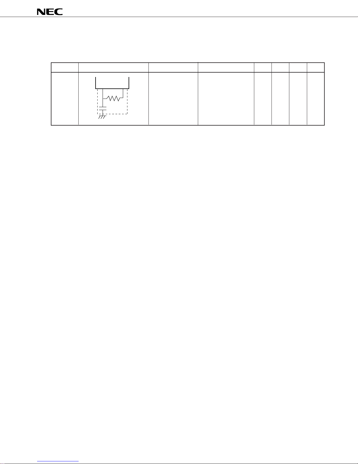
System Clock Oscillator Characteristics (T
Resonator
RC Oscillation 0.4 2.0 MHz
oscillator
Recommended Constant Parameter Testing Conditions MIN. TYP. MAX. Unit
CL1 CL2
A = –40 to +85 °C, VDD = 1.8 to 6.0 V)
frequency (fcc)
Note
•
Note Only the oscillator characteristics are shown. For the instruction execution time and oscillation frequency
characteristics, refer to AC Characteristics.
Caution When using the oscillation circuit of the system clock, wire the portion enclosed in dotted lines
in the figures as follows to avoid adverse influences on the wiring capacitance:
• Keep the wire length as short as possible.
• Do not cross other signal lines.
• Do not route the wiring in the vicinity of lines though which a high fluctuating current flows.
• Always keep the ground point of the capacitor of the oscillation circuit as the same potential
as V
SS.
• Do not connect the power source pattern through which a high current flows.
• Do not extract signals from the oscillation circuit.
Data Sheet U10040EJ2V1DS
49
µ
*
PD754144, 754244
• µPD754144
DC Characteristics (TA = –40 to +85°C, VDD = 1.8 to 6.0 V)
Parameter Symbol Conditions MIN. TYP. MAX. Unit
High-level output I
current P60 to P63, P80
Low-level output IOL Per pin 15 mA
current Total of all pins 45 mA
High-level input VIH1 Port 3 2.7 V ≤ VDD ≤ 6.0 V 0.7VDD VDD V
voltage 1.8 V ≤ VDD < 2.7 V 0.9VDD VDD V
Low-level input VIL1 Port 3 2.7 V ≤ VDD ≤ 6.0 V 0 0.3VDD V
voltage 1.8 V ≤ VDD < 2.7 V 0 0.1VDD V
High-level VOH VDD = 4.5 to 6.0 V, IOH = –1.0 mA VDD – 1.0 V
output voltage VDD = 1.8 to 6.0 V, IOH = –100 µAVDD – 0.5 V
Low-level VOL VDD = 4.5 to 6.0 V Port 3, IOL = 15 mA 0.6 2.0 V
output voltage Ports 6, 8, 0.4 V
High-level input ILIH VIN = VDD 3.0
leakage current
Low-level input I
leakage current
High-level output I
leakage current
Low-level output ILOL VOUT = 0 V –3.0
leakage current
On-chip pull-up RL1 VIN = 0 V Ports 3, 6, 8 50 100 200 kΩ
resistance RL2 Port 7, RESET 50 100 200 kΩ
OH Per pin P30, P31, P33, –5 mA
DD = 3.0 V, –7 –15 mA
P32, V
VOH = VDD – 2.0 V
Total of all pins –20 mA
VIH2 Ports 6 to 8, 2.7 V ≤ VDD ≤ 6.0 V 0.8VDD VDD V
KRREN, RESET 1.8 V ≤ VDD < 2.7 V 0.9VDD VDD V
VIL2 Ports 6 to 8, 2.7 V ≤ VDD ≤ 6.0 V 0 0.2VDD V
KRREN, RESET 1.8 V ≤ VDD < 2.7 V 0 0.1VDD V
IOL = 1.6 mA
VDD = 1.8 to 6.0 V, IOH = 400 µA 0.5 V
LIL VIN = 0 V –3.0
LOH VOUT = VDD 3.0
(mask option)
µ
A
µ
A
µ
A
µ
A
50 Data Sheet U10040EJ2V1DS
• µPD754144
*
µ
PD754144, 754244
DC Characteristics (T
Parameter Symbol Conditions MIN. TYP. MAX. Unit
Power supply IDD1 1.0-MHz VDD = 5.0 V ± 10%
Note 1
current
A = –40 to +85°C, VDD = 1.8 to 6.0 V)
Note 2
RC oscillation VDD = 3.0 V ± 10%
IDD2 R = 22 kΩ HALT VDD = 5.0 V ± 10% 0.5 1.8 mA
C = 22 pF mode VDD = 3.0 V ± 10% 0.25 0.9 mA
IDD1 1.0-MHz VDD = 5.0 V ± 10%
RC oscillation VDD = 3.0 V ± 10%
IDD2 R = 5.1 kΩ HALT VDD = 5.0 V ± 10% 0.95 2.8 mA
C = 120 pF mode VDD = 3.0 V ± 10% 0.5 1.5 mA
IDD3 STOP VDD = 1.8 to 6.0 V 5
mode TA = 25°C1
VDD = 3.0 V ±10% 0.1 3
Note 3
Note 2
Note 3
TA = –40 to +40°C 0.1 1
0.7 2.1 mA
0.3 1.0 mA
1.15 3.5 mA
0.55 1.6 mA
µ
µ
µ
µ
A
A
A
A
Notes 1. The current flowing through the on-chip pull-up resistor, the current during EEPROM writing time, and
the current when the program threshold port (PTH) is operating are not included.
2. When the device is operated in the high-speed mode by setting the processor clock control register
(PCC) to 0011H.
3. When the device is operated in the low-speed mode by setting PCC to 0000H.
Data Sheet U10040EJ2V1DS
51

• µPD754144
*
µ
PD754144, 754244
AC Characteristics (T
A = –40 to +85°C, VDD = 1.8 to 6.0 V)
Parameter Symbol Test Conditions MIN. TYP. MAX. Unit
CPU clock cycle time
Note1
tCY
2.0 4.0 128
(Minimum instruction execution
time = 1 machine cycle)
RC oscillation frequency fCC R = 22 kΩ, VDD = 3.6 to 6.0 V 0.9 1.0
C = 22 pF VDD = 2.2 to 3.6 V 0.75 1.0
VDD = 1.8 to 3.6 V 0.5 1.0
VDD = 1.8 to 6.0 V 0.5 1.0
R = 5.1 kΩ, VDD = 3.6 to 6.0 V 0.91 1.0
C = 120 pF VDD = 2.2 to 3.6 V 0.76 1.0
VDD = 1.8 to 3.6 V 0.51 1.0
VDD = 1.8 to 6.0 V 0.51 1.0
Interrupt input high- and
tINTH, tINTL
INT0 IM02 = 0 Note 3
low-level width IM02 = 1 10
KR4 to KR7 10
RESET low-level width tRSL 10
Note 2
Note 2
Note 2
Note 2
Note 2
Note 2
Note 2
Note 2
µ
s
1.2 MHz
1.15 MHz
1.15 MHz
1.2 MHz
1.1 MHz
1.05 MHz
1.05 MHz
1.1 MHz
µ
s
µ
s
µ
s
µ
s
Notes 1. The CPU clock (Φ) cycle time (minimum
instruction execution time) is determined
by the time constants of the connected
resistor (R) and capacitor (d) and the pro-
cessor clock control register (PCC). The
figure on the right shows the cycle time t
CY
characteristics against the supply voltage
VDD when the system clock is used.
2. This is the typical value when VDD = 3.6 V.
3. 2tCY or 128/fCC depending on the setting of
the interrupt mode register (IM0).
128
6
5
4
µ
( s)
3
CY
2
Cycle time t
1
t
CY
vs. V
DD
(During system clock operation)
Operation guranteed range
52 Data Sheet U10040EJ2V1DS
0.5
1234561.8
0
DD
Supply voltage V
(V)

• µPD754144
*
µ
PD754144, 754244
EEPROM Characteristics (T
A = –40 to +85°C, VDD = 1.8 to 6.0 V)
Parameter Symbol Conditions MIN. TYP. MAX. Unit
EEPROM IEEW 1.0 MHz, VDD = 5.0 V ± 10% 4.0 12 mA
write current RC oscillation VDD = 3.0 V ± 10% 2.0 6 mA
EEPROM t
write time
EEPROM EEWT TA = –40 to +70°C100000 times/byte
write times T
EEW 1.0 MHz, RC oscillation
A = –40 to +85°C 80000 times/byte
Note
3.8 4.6 10.0 ms
Note Set EWTC 4 to 6 so as to be 18 x 28/fCC (4.6 ms: @ fCC = 1.0-MHz operation), considering the variation
of the RC oscillation.
Comparator Characteristics (TA = –40 to +85°C, VDD = 1.8 to 6.0 V)
Parameter Symbol Conditions MIN. TYP. MAX. Unit
Comparison accuracy VACOMP ±100 mV
Threshold voltage VTH Note Note V
PTH input voltage VIPTH 0VDD V
AVREF input voltage VIAVREF 1.8 VDD V
Comparator circuit I
current consumption
DD5 When bit 7 of PTHM is set to 1 1 mA
Note The threshold voltage becomes as follows by settings bits 0 to 3 of PTHM.
VTH = VIAVREF x (n + 0.5)/16 (n = 0 to 15)
Data Sheet U10040EJ2V1DS
53
• µPD754144
*
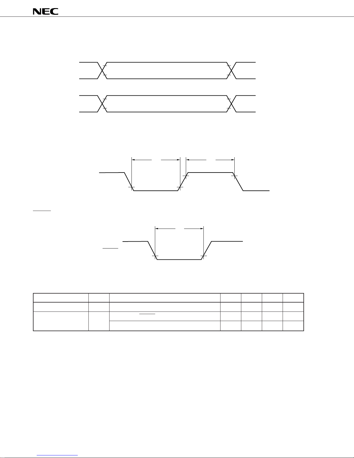
AC Timing Test Points
µ
PD754144, 754244
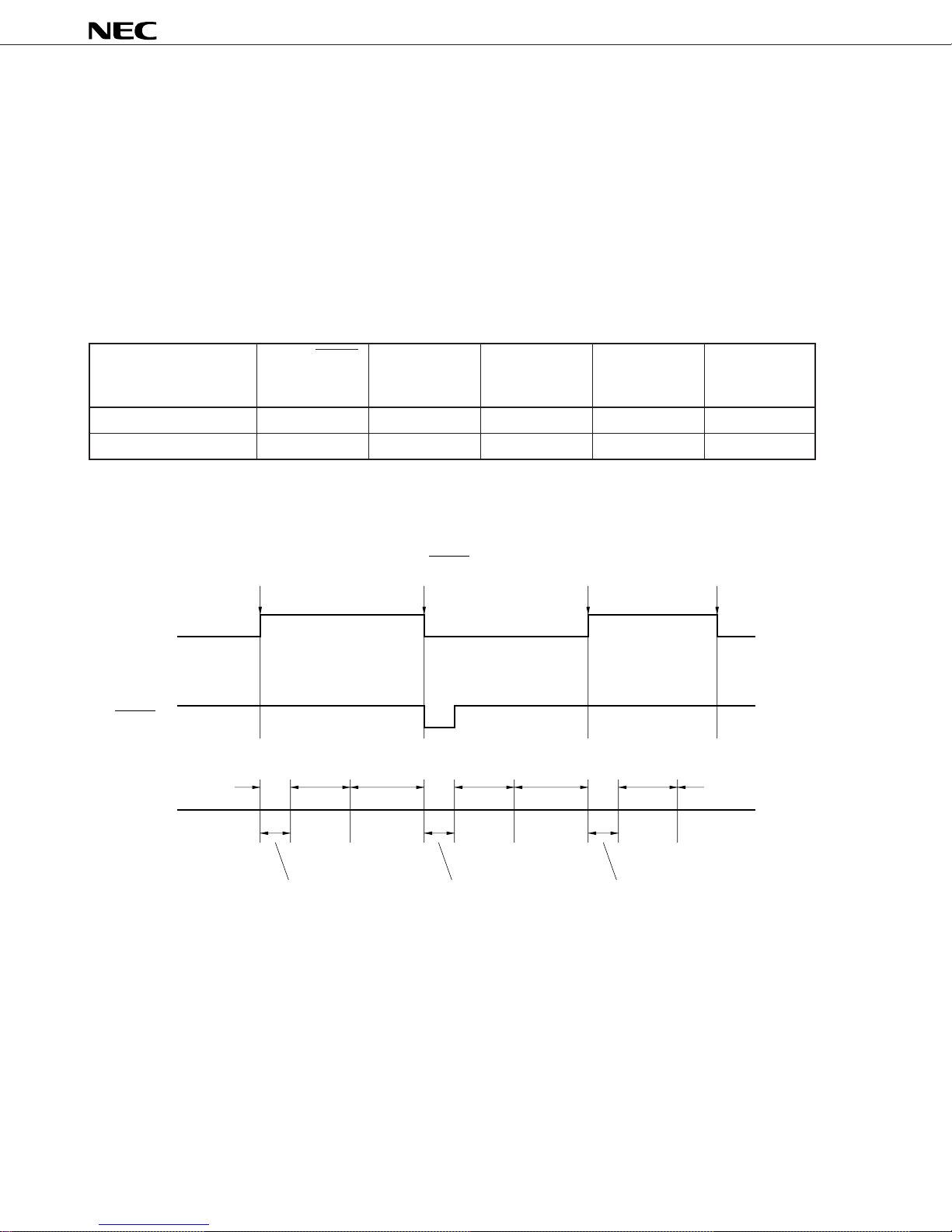
Interrupt Input Timing
INT0, KR4 to KR7
RESET Input Timing
VIH (MIN.)
IL
(MAX.)
V
VOH (MIN.)
OL
(MAX.)
V
t
INTL
V
IH
(MIN.)
IL
(MAX.)
V
V
OH
(MIN.)
OL
(MAX.)
V
t
INTH
t
RSL
RESET
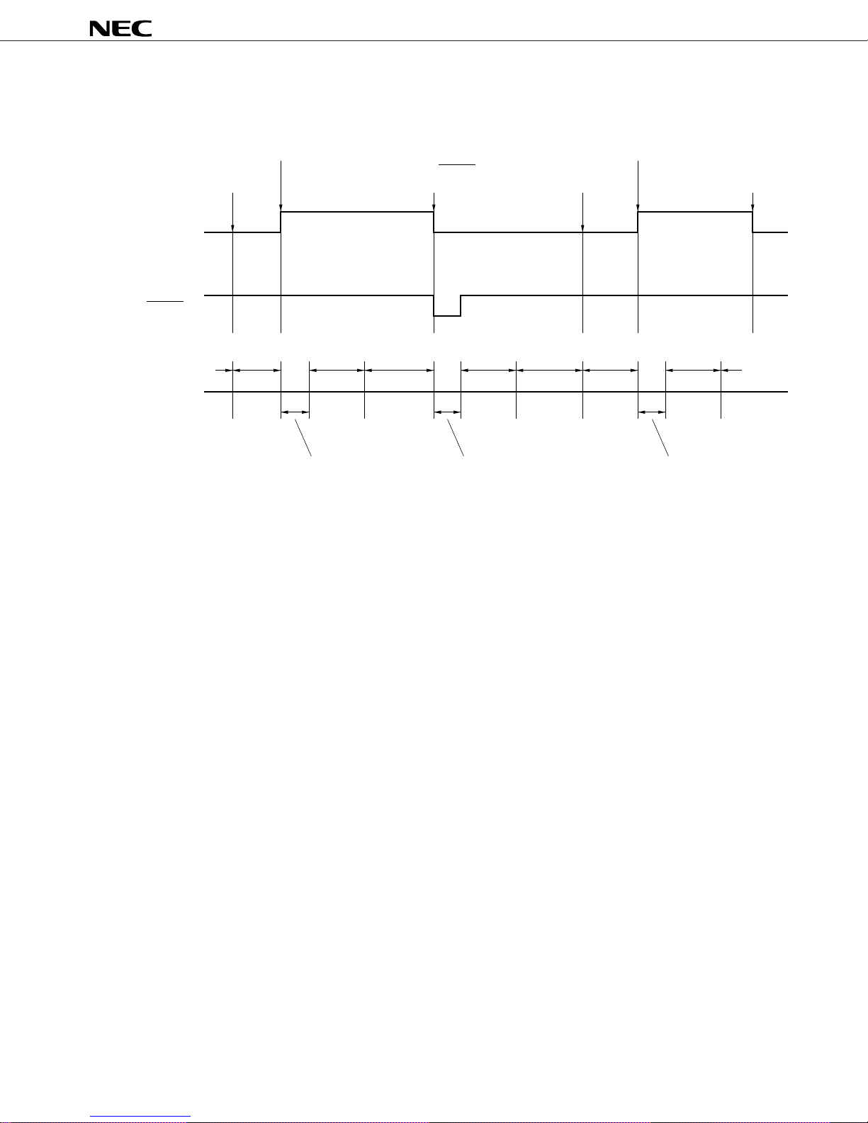
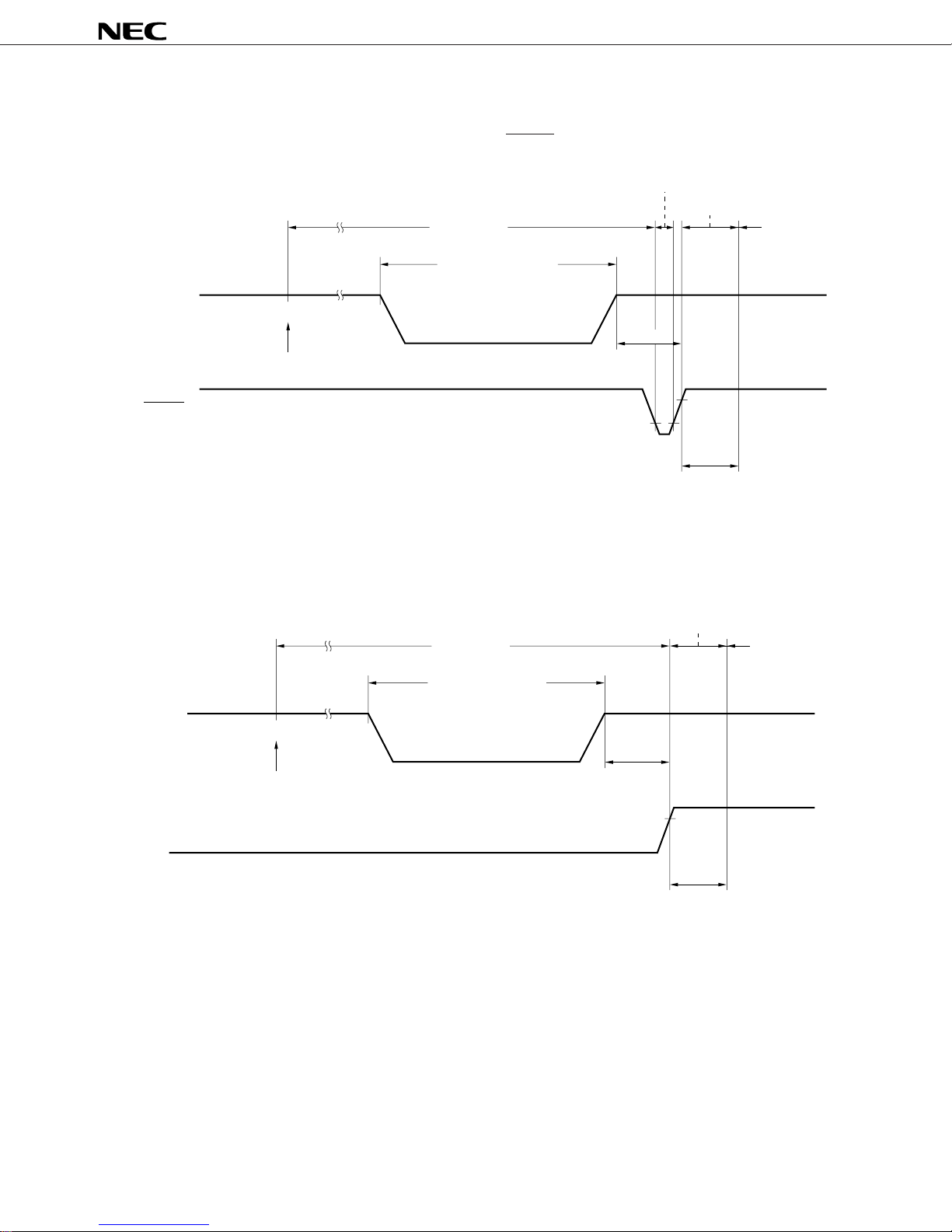
Data Memory STOP Mode Low-Supply Voltage Data Retention Characteristics (T
A = –40 to +85°C)
Parameter Symbol Test Conditions MIN. TYP. MAX. Unit
Release signal set time tSREL 0
Oscillation stabilization tWAIT Release by RESET 56/fCC
wait time Release by interrupt request 512/f
CC
µ
s
µ
s
µ
s
54 Data Sheet U10040EJ2V1DS
• µPD754144
*
Data Retention Timing (on releasing STOP mode by RESET)
STOP mode
Data retention mode
V
DD
Execution of STOP instruction
RESET
µ
PD754144, 754244
Internal reset operation
HALT mode
t
SREL
WAIT
t
Operation mode
Data Retention Timing (Standby release signal: on releasing STOP mode by interrupt signal)
HALT mode
V
DD
Execution of STOP instruction
Standby release signal
(interrupt request)
STOP mode
Data retention mode
t
SREL
t
WAIT
Operation mode
Data Sheet U10040EJ2V1DS
55

13.2 µPD754244
*
µ
PD754144, 754244
Absolute Maximum Ratings (T
Parameter Symbol Test Conditions Ratings Unit
Power supply voltage VDD –0.3 to +7.0 V
Input voltage VI –0.3 to VDD + 0.3 V
Output voltage VO –0.3 to VDD + 0.3 V
Output current, high IOH Per pin P30, P31, P33, P60 to P63, P80 –10 mA
Output current, low IOL
Operating ambient T
temperature
Storage temperature T
Note
A –40 to +85 °C
stg –65 to +150 °C
A = 25°C)
P32 –20 mA
For all pins –30 mA
Per pin 20 mA
For all pins 90 mA
Caution If any of the parameters exceeds the absolute maximum ratings, even momentarily, the quality
of the product may be impaired. The absolute maximum ratings are values that may physically
damage the products. Be sure to use the products within the ratings.
Capacitance (T
A = 25°C, VDD = 0 V)
Parameter Symbol Test Conditions MIN. TYP. MAX. Unit
Input capacitance CIN f = 1 MHz 15 pF
Output capacitance COUT Unmeasured pins returned to 0 V 15 pF
I/O capacitance C
IO 15 pF
56 Data Sheet U10040EJ2V1DS
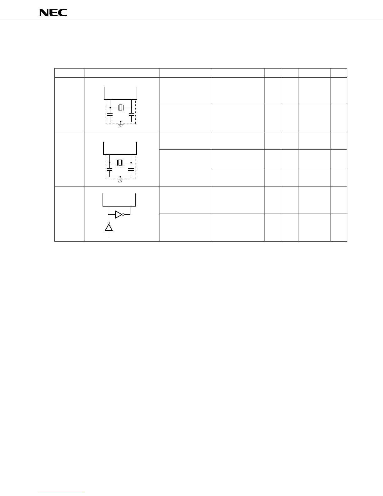
• µPD754244
*
µ
PD754144, 754244
System Clock Oscillator Characteristics (T
Resonator
Ceramic Oscillation 1.0
resonator
Crystal Oscillation 1.0 6.0
resonator
External X1 input 1.0 6.0
clock frequency (f
Recommended Constant Parameter Testing Conditions MIN. TYP. MAX. Unit
X1 X2
C1 C2
X1 X2
C1 C2
X1 X2
A = –40 to +85°C, VDD = 1.8 to 6.0 V)
X)
Note1
After VDD reaches MIN.
voltage range
Note1
Note3
Note1
frequency (fX)
Oscillation
stabilization value of oscillation
Note 5
time
frequency(fX)
Oscillation VDD = 4.5 to 6.0 V 10 ms
stabilization time
X1 input high- and 83.3 500 ns
low-level widths
(t
XH, tXL)
Notes2, 3, 4
6.0
4ms
Notes2, 3, 4
30 ms
Notes2, 3, 4
MHz
MHz
MHz
Notes 1. Only the oscillator characteristics are shown. For the instruction execution time, refer to AC Charac-
teristics.
2. If the oscillation frequency is 2.1 MHz < f
X ≤ 4.19 MHz at 1.8 V ≤ VDD < 2.0 V, set the processor control
register (PCC) to a value other than 0011. If the PCC is set to 0011, the rated machine cycle time
of 1.9
µ
s is not satisfied.
3. If the oscillation frequency is 4.19 MHz < f
X ≤ 6.0 MHz at 1.8 V≤ VDD < 2.0 V, set the processor control
register (PCC) to a value other than 0011 or 0010. If the PCC is set to 0011 or 0010, the rated machine
cycle time of 1.9 µs is not satisfied.
4. If the oscillation frequency is 4.19 MHz < f
X ≤ 6.0 MHz at 2.0 V≤ VDD < 2.7 V, set the processor control
register (PCC) to a value other than 0011. If the PCC is set to 0011, the rated machine cycle time of
0.95
µ
s is not satisfied.
5. Oscillation stabilization time is a time required for oscillation to stabilize after application of V
DD,
or after the STOP mode has been released.
Caution When using the oscillation circuit of the system clock, wire the portion enclosed in dotted lines
in the figures as follows to avoid adverse influences on the wiring capacitance:
• Keep the wire length as short as possible.
• Do not cross other signal lines.
• Do not route the wiring in the vicinity of lines though which a high fluctuating current flows.
• Always keep the ground point of the capacitor of the oscillation circuit as the same potential
as V
SS.
• Do not connect the power source pattern through which a high current flows.
• Do not extract signals from the oscillation circuit.
Data Sheet U10040EJ2V1DS
57

• µPD754244
*
Recommended Oscillator Constants
µ
PD754144, 754244
Ceramic resonator (T
Manufacturer Part Number Frequency Recommended Circuit Oscillation Voltage Remark
Kyocera KBR-1000F/Y 1.0 100 100 1.8 6.0 —
KBR-2.0MS 2.0 47 47
KBR-4.19MSB 4.19 33 33
KBR-4.19MKC — — Model with capacitor
PBRC4.19A 33 33 —
PBRC4.19B — — Model with capacitor
KBR-6.0MSB 6.0 33 33 —
KBR-6.0MKC — — Model with capacitor
PBRC6.00A 33 33 —
PBRC6.00B — — Model with capacitor
A = –20 to +80°C)
Constant (pF) Range (VDD)
(MHz) C1 C2 MN. (V) MAX. (V)
Ceramic resonator (TA = –40 to +80°C)
Manufacturer Part Number Frequency Recommended Circuit Oscillation Voltage Remark
Constant (pF) Range (VDD)
(MHz) C1 C2 MIN. (V) MAX. (V)
Murata Mfg. CSB1000J
Co., Ltd. CSA2.00MG040 2.0 —
CST2.00MG040 — — Model with capacitor
CSA4.19MG 4.19 30 30 1.9 —
CST4.19MGW — — Model with capacitor
CSA4.19MGU 30 30 1.8 —
CST4.19MGWU — — Model with capacitor
CSA6.00MG 6.0 30 30 2.5 —
CST6.00MGW — — Model with capacitor
CSA6.00MGU 30 30 1.8 —
CST6.00MGWU — — Model with capacitor
TDK CCR1000K2 1.0 100 100 2.0 —
CCR4.19MC3 4.19 — — Model with capacitor
FCR4.19MC5
CCR6.0MC3 6.0
FCR6.0MC5
Note
1.0 100 100 2.0 6.0 Rd = 2.2 kΩ
58 Data Sheet U10040EJ2V1DS
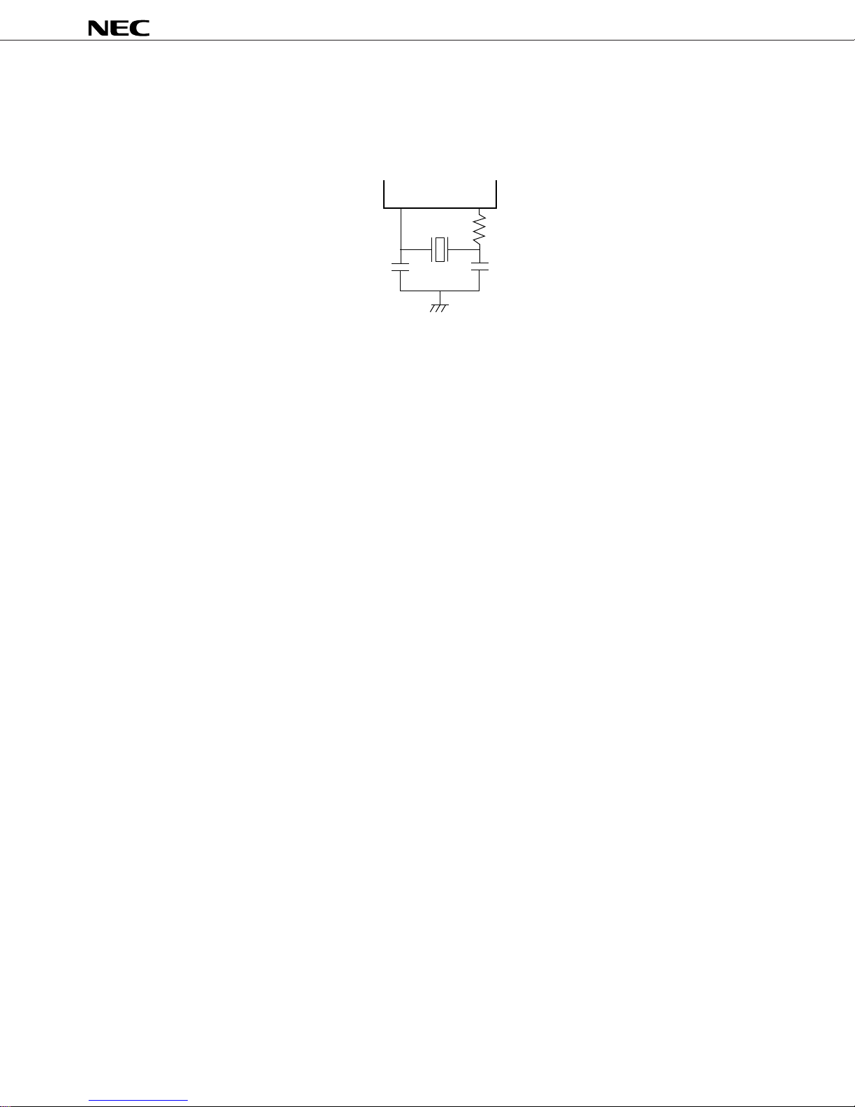
µ
*
PD754144, 754244
Note When using the CSB1000J (1.0 MHz) made by Murata Mfg. Co., Ltd. as a ceramic resonator, a limiting
resistor (Rd = 2.2 kΩ) is necessary (refer to the figure below). This resistor is not necessary when using
the other recommended resonators.
X1 X2
CSB1000J
•
C1
Rd
•
C2
•
Caution The oscillator constants and oscillation voltage range indicate conditions for stable oscilla-
tion, but do not guarantee oscillation frequency accuracy. If oscillation frequency accuracy is
required for actual circuits, it is necessary to adjust the oscillation frequency of the oscillator
in the actual circuit. Please contact directly the manufacturer of the resonator to be used.
Data Sheet U10040EJ2V1DS
59

µ
*
PD754144, 754244
• µPD754244
DC Characteristics (TA = –40 to +85°C, VDD = 1.8 to 6.0 V)
Parameter Symbol Conditions MIN. TYP. MAX. Unit
High-level output I
current P60 to P63, P80
Low-level output IOL Per pin 15 mA
current Total of all pins 45 mA
High-level input VIH1 Port 3 2.7 V ≤ VDD ≤ 6.0 V 0.7VDD VDD V
voltage 1.8 V ≤ VDD < 2.7 V 0.9VDD VDD V
Low-level input VIL1 Port 3 2.7 V ≤ VDD ≤ 6.0 V 0 0.3VDD V
voltage 1.8 V ≤ VDD < 2.7 V 0 0.1VDD V
High-level VOH VDD = 4.5 to 6.0 V, IOH = –1.0 mA VDD – 1.0 V
output voltage VDD = 1.8 to 6.0 V, IOH = –100 µAVDD – 0.5 V
Low-level VOL VDD = 4.5 to 6.0 V Port 3, IOL = 15 mA 0.6 2.0 V
output voltage Ports 6, 8, 0.4 V
High-level input ILIH1 VIN = VDD Pins other than X1 3.0 µA
leakage current ILIH2 X1 20 µA
Low-level input ILIL1 VIN = 0 V Pins other than X1 –3.0 µA
leakage current ILIH2 X1 –20 µA
High-level output I
leakage current
Low-level output I
leakage current
On-chip pull-up RL1 VIN = 0 V Port 3, 6, 8 50 100 200 kΩ
resistance R
OH Per pin P30, P31, P33, –5 mA
DD = 3.0 V, –7 –15 mA
P32, V
VOH = VDD – 2.0 V
Total of all pins –20 mA
VIH2 Ports 6 to 8, 2.7 V ≤ VDD ≤ 6.0 V 0.8VDD VDD V
KRREN, RESET 1.8 V ≤ VDD < 2.7 V 0.9VDD VDD V
VIH3 X1 VDD – 0.1 VDD V
VIL2 Ports 6 to 8, 2.7 V ≤ VDD ≤ 6.0 V 0 0.2VDD V
KRREN, RESET 1.8 V ≤ VDD < 2.7 V 0 0.1VDD V
VIH3 X1 0 0.1 V
IOL = 1.6 mA
VDD = 1.8 to 6.0 V, IOH = 400 µA 0.5 V
LOH VOUT = VDD 3.0 µA
LOL VOUT = 0 V –3.0 µA
L2 Port 7, RESET 50 100 200 kΩ
(mask option)
60 Data Sheet U10040EJ2V1DS

• µPD754244
*
µ
PD754144, 754244
DC Characteristics (T
Parameter Symbol Conditions MIN. TYP. MAX. Unit
Power supply IDD1 4.19-MHz VDD = 5.0 V ± 10%
Note 1
current
A = –40 to +85°C, VDD = 1.8 to 6.0 V)
Note 2
crystal VDD = 3.0 V ± 10%
IDD2 oscillation HALT VDD = 5.0 V ± 10% 0.64 3.0 mA
C1 = C2 = 22 pF mode VDD = 3.0 V ± 10% 0.20 0.9 mA
IDD3 X1 = 0 V VDD = 1.8 to 6.0 V 5
STOP mode TA = 25°C1
VDD = 3.0 V ± 10% 0.1 3
Note 3
A = –40 to +40°C 0.1 1
T
1.5 5.0 mA
0.23 1.0 mA
µ
µ
µ
µ
A
A
A
A
Notes 1. The current flowing through the on-chip pull-up resistor, the current during EEPROM writing time, and
the current during the program threshold port (PTH) operation are not included.
2. When the device is operated in the high-speed mode by setting the processor clock control register
(PCC) to 0011H
3. When the device is operated in the low-speed mode by setting PCC to 0000H
Data Sheet U10040EJ2V1DS
61
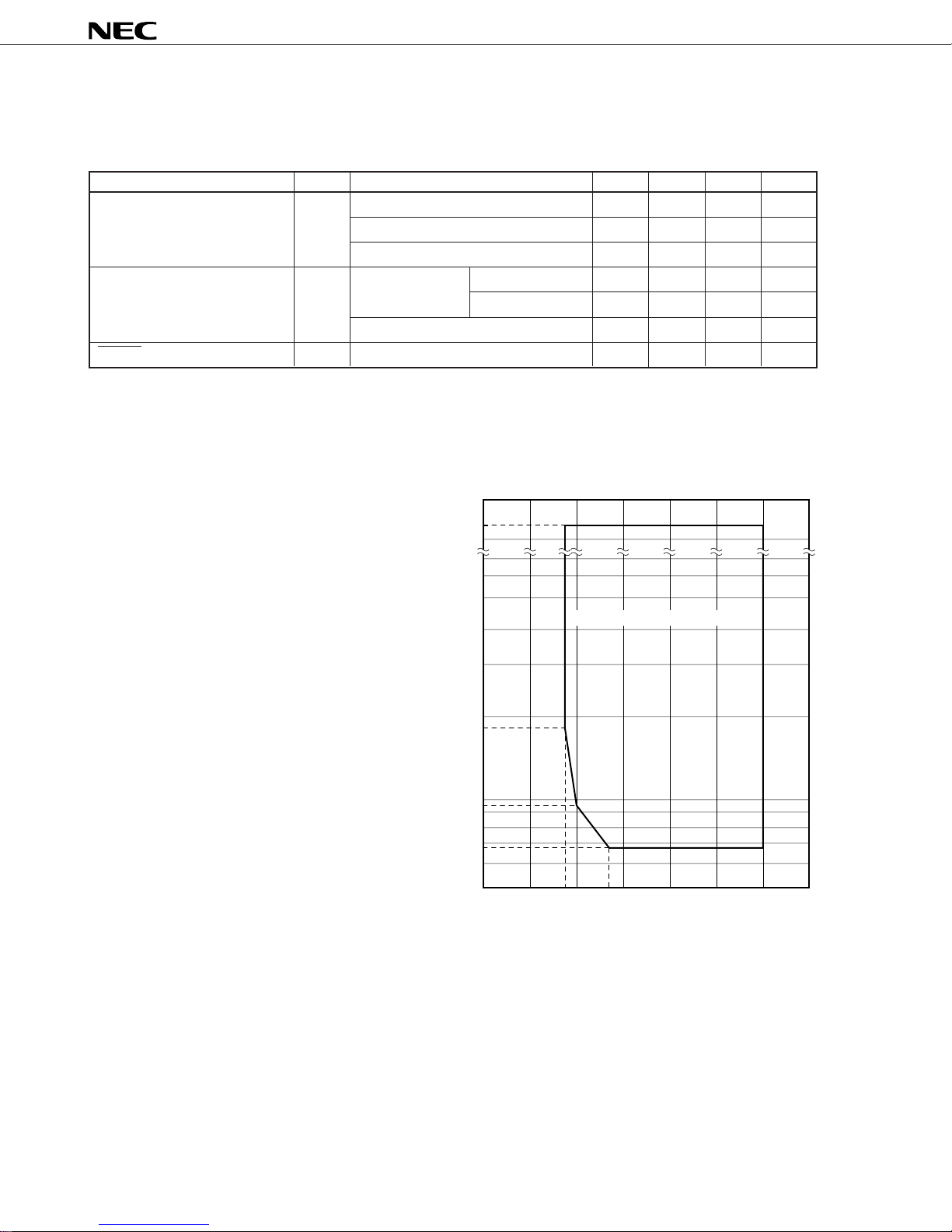
• µPD754244
pply
)
*
µ
PD754144, 754244
AC Characteristics (T
Parameter Symbol Test Conditions MIN. TYP. MAX. Unit
CPU clock cycle time
(Minimum instruction execution VDD = 2.0 to 2.7 V 0.95 64.0
time = 1 machine cycle) VDD = 2.7 to 6.0 V 0.67 64.0
Interrupt input high- and
low-level width IM02 = 1 10
RESET low-level width t
A = –40 to +85°C, VDD = 1.8 to 6.0 V)
Note 1
tCY VDD = 1.8 to 2.0 V 1.9 64.0
tINTH, tINTL
RSL 10
INT0 IM02 = 0 Note 2
KR4 to KR7 10
Notes 1. The CPU clock (Φ) cycle time (minimum
instruction execution time) is determined
by the oscillation frequency of the con-
nected resonator (or external clock) and
the processor clock control register (PCC).
The figure on the right shows the cycle
time t
CY characteristics against the supply
64
60
t
CY vs. VDD
(During system clock operation)
voltage VDD when the system clock is used.
2. 2t
CY or 128/fX depending on the setting of
the interrupt mode register (IM0).
6
5
4
µ
3
Operation guranteed range
µ
s
µ
s
µ
s
µ
s
µ
s
µ
s
µ
s
1.9
Cycle time tCY ( s)
0.95
0.67
0.5
2
1
0
123456
1.8
2.7
Su
voltage VDD (V
62 Data Sheet U10040EJ2V1DS
• µPD754244
*
µ
PD754144, 754244
EEPROM Characteristics (T
A = –40 to +85°C, VDD = 1.8 to 6.0 V)
Parameter Symbol Conditions MIN. TYP. MAX. Unit
EEPROM IEEW 4.19 MHz, VDD = 5.0 V ± 10% 4.5 15 mA
write current crystal oscillation VDD = 3.0 V ± 10% 2.0 6 mA
EEPROM t
write time
EEPROM EEWT TA = –40 to +70°C100000 times/byte
write times T
EEW 3.8 10.0 ms
A = –40 to +85°C 80000 times/byte
Comparator Characteristics (TA = –40 to +85°C, VDD = 1.8 to 6.0 V)
Parameter Symbol Conditions MIN. TYP. MAX. Unit
Comparison accuracy VACOMP ±100 mV
Threshold voltage VTH Note Note V
PTH input voltage VIPTH 0VDD V
AVREF input voltage VIAVREF 1.8 VDD V
Comparator circuit I
current consumption
DD5 When bit 7 of PTHM is set to 1 1 mA
Note The threshold voltage becomes as follows by settings bits 0 to 3 of PTHM.
VTH = VIAVREF x (n + 0.5)/16 (n = 0 to 15)
Data Sheet U10040EJ2V1DS
63
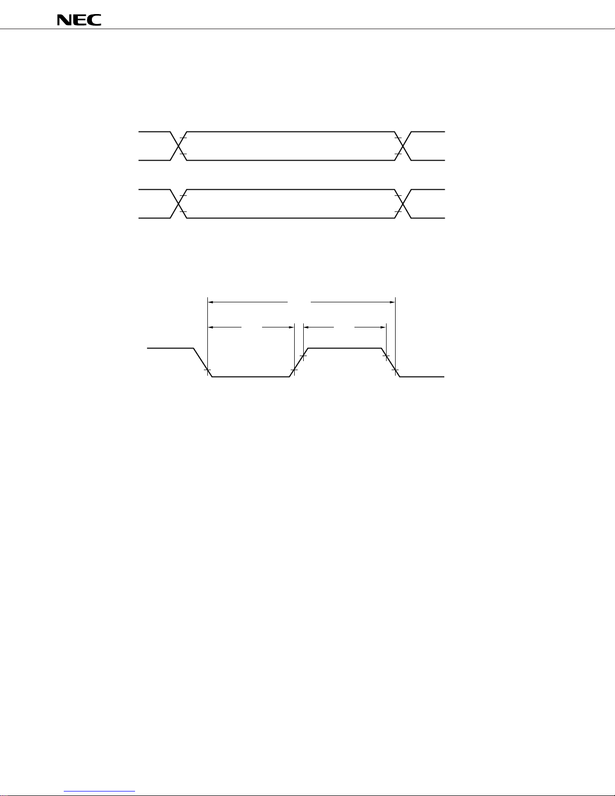
• µPD754244
*
AC Timing Test Points (Excluding X1 Input)
µ
PD754144, 754244
Clock Timing
X1 input
VIH (MIN.)
IL
(MAX.)
V
VOH (MIN.)
OL
(MAX.)
V
V
IH
(MIN.)
IL
(MAX.)
V
V
OH
(MIN.)
OL
(MAX.)
V
1/f
X
t
XL
t
XH
VDD– 0.1 V
0.1 V
64 Data Sheet U10040EJ2V1DS
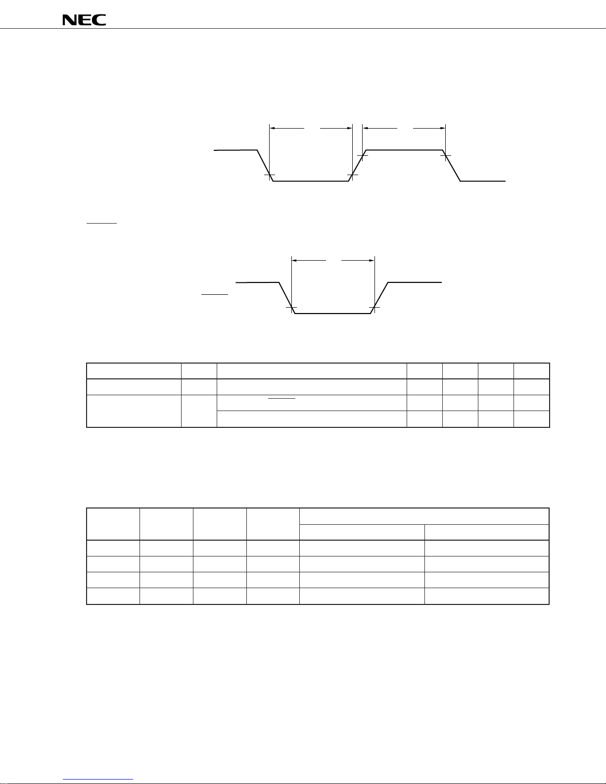
• µPD754244
*
Interrupt Input Timing
µ
PD754144, 754244
INTL
t
t
INTH
INT0, KR4 to KR7
RESET Input Timing
t
RSL
RESET
Data Memory STOP Mode Low-Supply Voltage Data Retention Characteristics (T
Parameter Symbol Test Conditions MIN. TYP. MAX. Unit
Release signal set time tSREL 0
Oscillation stabilization tWAIT Release by RESET Note 2 ms
wait time
Note 1
Release by interrupt request Note 3 ms
A = –40 to +85 °C)
µ
s
Notes 1. The oscillation stabilization wait time is the time during which the CPU operation is stopped to
avoid unstable operation at oscillation start.
17
2. 2
/fx and 215/fx can be selected with mask option.
3. Depends on setting of basic interval timer mode register (BTM) (see table below).
BTM3 BTM2 BTM1 BTM0 Wait Time
When fX = 4.19 MHz When fX = 6.0 MHz
–0002
–0112
–1012
–1112
20
/fX (Approx. 250 ms) 220/fX (Approx. 175 ms)
17
/fX (Approx. 31.3 ms) 217/fX (Approx. 21.8 ms)
15
/fX (Approx. 7.81 ms) 215/fX (Approx. 5.46 ms)
13
/fX (Approx. 1.95 ms) 213/fX (Approx. 1.37 ms)
Data Sheet U10040EJ2V1DS
65
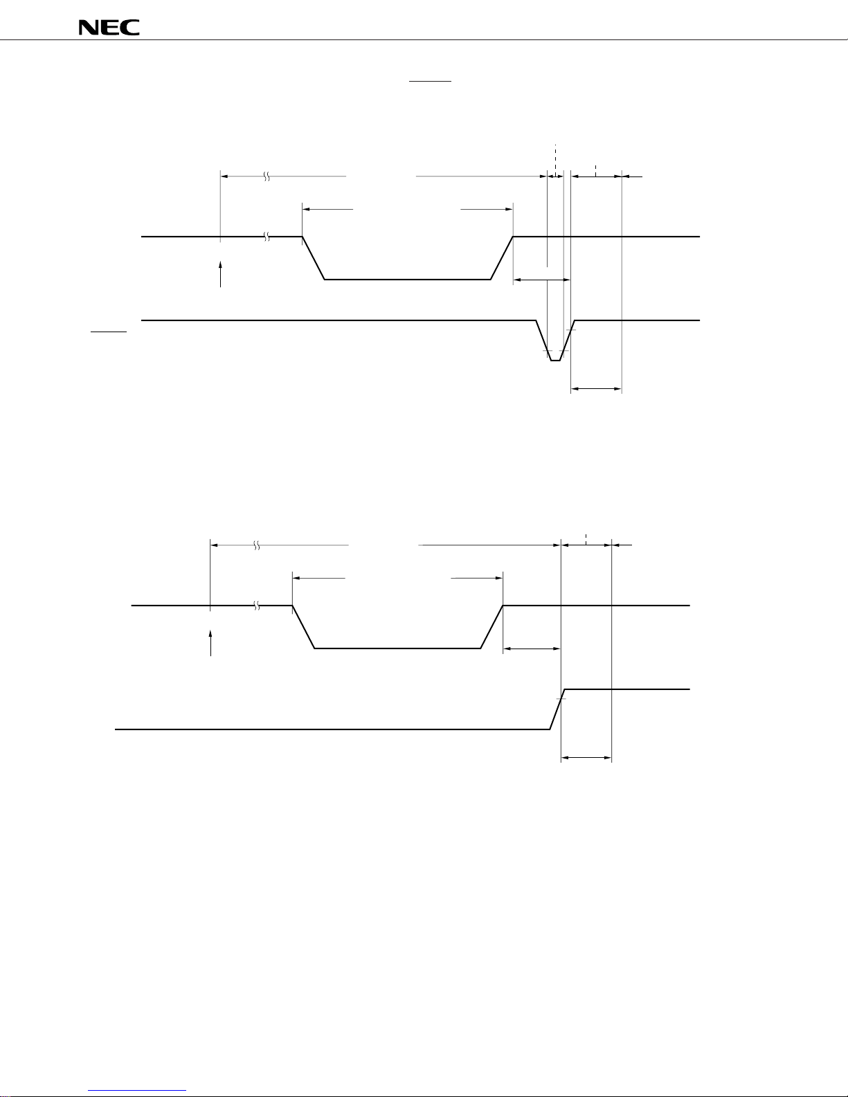
Data Retention Timing (on releasing STOP mode by RESET)
*
STOP mode
Data retention mode
V
DD
Execution of STOP instruction
RESET
µ
PD754144, 754244
Internal reset operation
HALT mode
t
SREL
WAIT
t
Operation mode
Data Retention Timing (Standby release signal: on releasing STOP mode by interrupt signal)
HALT mode
V
DD
Execution of STOP instruction
Standby release signal
(interrupt request)
STOP mode
Data retention mode
t
SREL
t
WAIT
Operation mode
66 Data Sheet U10040EJ2V1DS
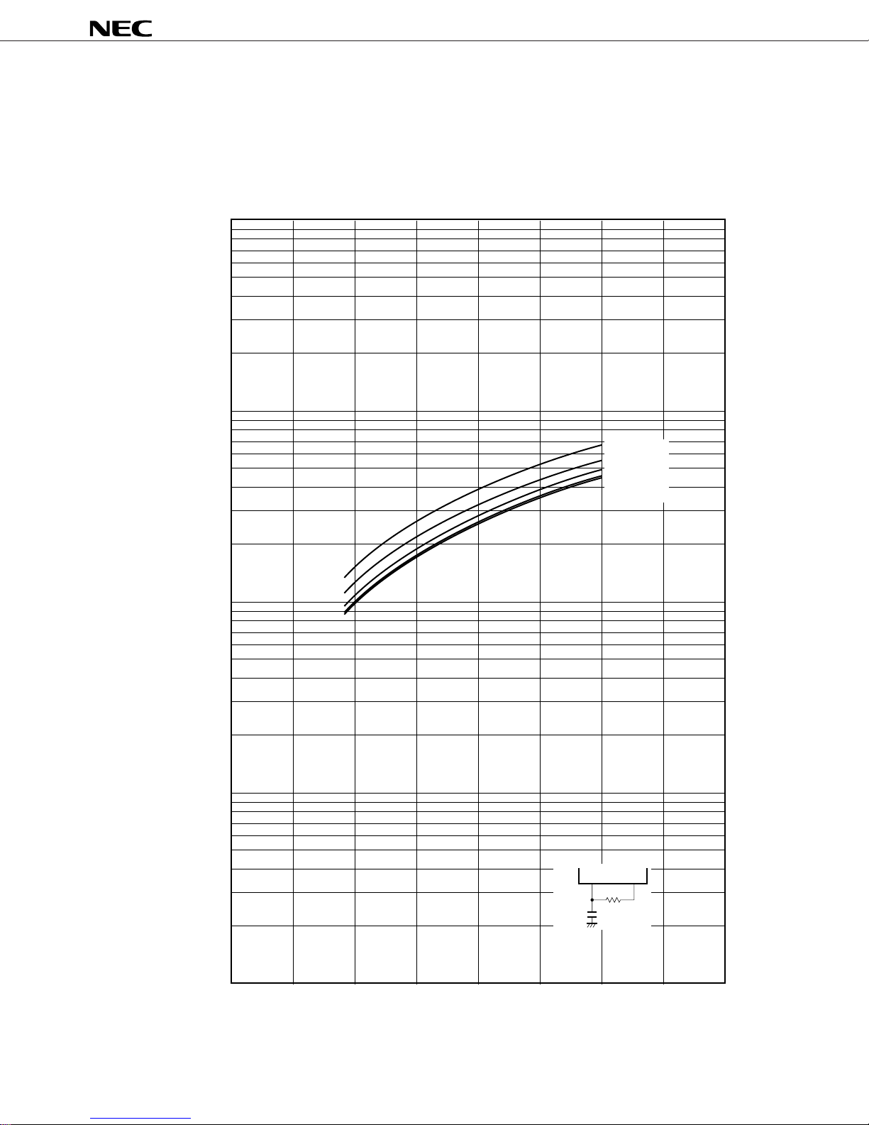
14. CHARACTERISTICS CURVES (REFERENCE VALUES)
*
14.1 µPD754144
IDD vs. VDD (RC Oscillation, R = 22 kΩ, C = 22 pF)
µ
PD754144, 754244
(mA)
DD
10
5.0
1.0
0.5
0.1
(TA = 25°C)
PCC = 0011
PCC = 0010
PCC = 0001
PCC = 0000
System clock HALT mode
0.05
Power Supply Current I
0.01
0.005
CL1 CL2
22 kΩ
22 pF
0.001
012345678
Power Supply Voltage VDD (V)
Data Sheet U10040EJ2V1DS
67

• µPD754144
)
*
10
5.0
1.0
0.5
IDD vs. VDD (RC Oscillation, R = 5.1 kΩ, C = 120 pF)
µ
PD754144, 754244
(T
A
= 25°C)
PCC = 0011
PCC = 0010
PCC = 0001
PCC = 0000 and
System clock HALT mode
(mA)
DD
0.1
0.05
Power Supply Current I
0.01
0.005
CL1 CL2
5.1 kΩ
120 pF
0.001
012345678
68 Data Sheet U10040EJ2V1DS
Power Supply Voltage VDD (V

14.2 µPD754244
*
10
5.0
µ
IDD vs. VDD (System Clock: 6.0-MHz Crystal Resonator)
PCC = 0011
PCC = 0010
PD754144, 754244
A = 25°C)
(T
Power Supply Current IDD (mA)
1.0
0.5
0.1
0.05
0.01
PCC = 0001
PCC = 0000
System clock HALT mode
0.005
0.001
012345678
Power Supply Voltage VDD (V)
Data Sheet U10040EJ2V1DS
22 pF
X1 X2
Crystal resonator
6.0 MHz
22 pF
69
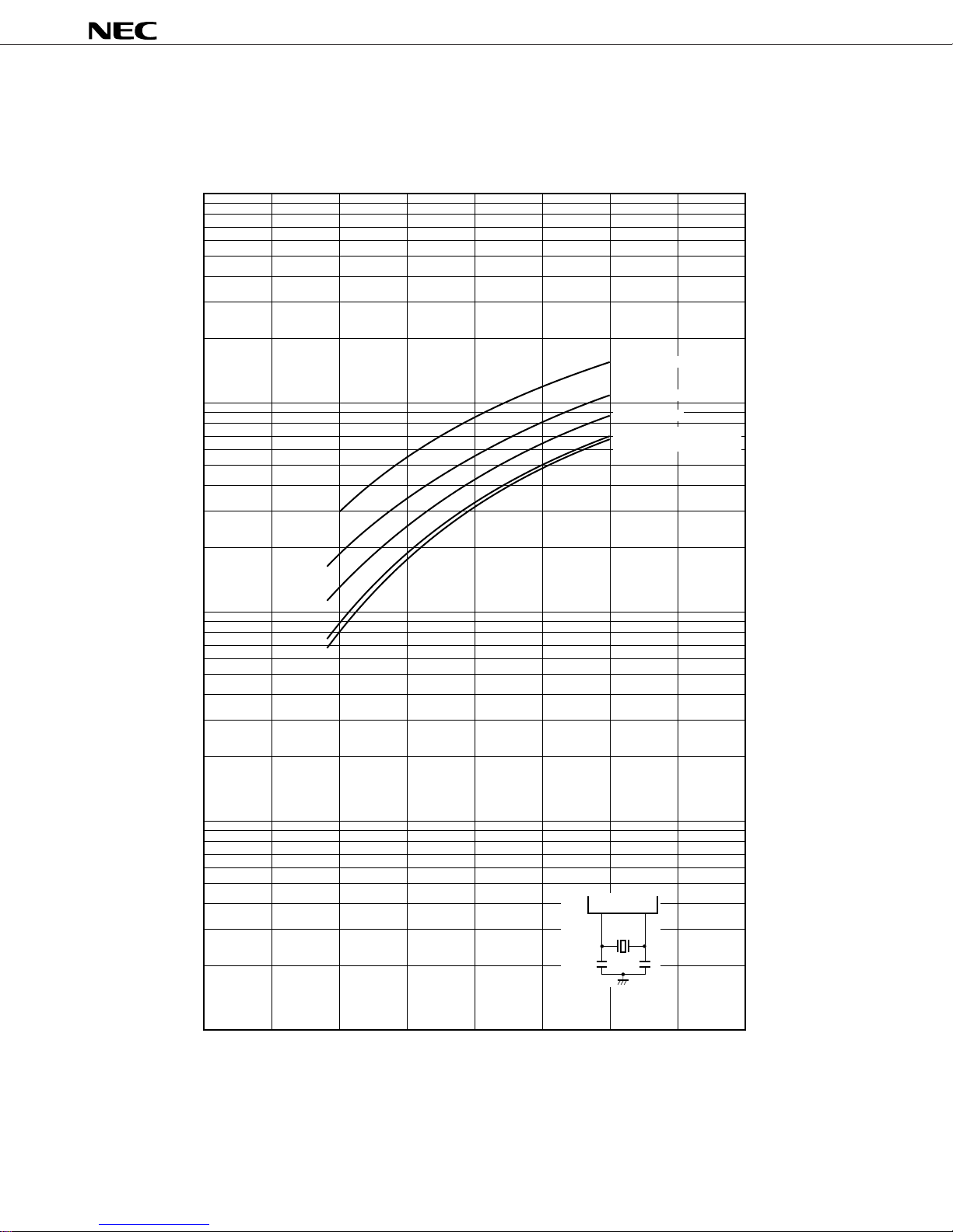
• µPD754244
)
*
10
5.0
IDD vs. VDD (System Clock: 4.19-MHz Crystal Resonator)
PCC = 0011
µ
PD754144, 754244
A = 25°C)
(T
Power Supply Current IDD (mA)
1.0
0.5
0.1
0.05
0.01
PCC = 0010
PCC = 0001
PCC = 0000
System clock HALT mode
0.005
0.001
012345678
70 Data Sheet U10040EJ2V1DS
Power Supply Voltage VDD (V
22 pF
X1 X2
Crystal resonator
4.19 MHz
22 pF

• µPD754244
*
10
5.0
µ
PD754144, 754244
IDD vs. VDD (System Clock: 2.0-MHz Crystal Resonator)
A
(T
= 25°C)
1.0
0.5
(mA)
DD
0.1
Power Supply Current I
0.05
0.01
PCC = 0011
PCC = 0010
PCC = 0001
PCC = 0000
System clock HALT mode
0.005
0.001
012345678
Power Supply Voltage VDD (V)
Data Sheet U10040EJ2V1DS
47 pF
X1 X2
Crystal resonator
2.0 MHz
47 pF
71

µ
*
PD754144, 754244
15. RC OSCILLATION FREQUENCY CHARACTERISTICS EXAMPLES (REFERENCE VALUES)
f
CC vs. VDD (RC Oscillation, R = 22 kΩ, C = 22 pF)
A = –40°C)
2.0
CL1 CL2
22 kΩ
22 pF
1.0
Sample C
Sample B
System Clock Frequency fCC (MHz)
(T
0.5
012345678
2.0
22 pF
1.0
System Clock Frequency fCC (MHz)System Clock Frequency fCC (MHz)
0.5
012345678
2.0
Sample A
CL1 CL2
22 kΩ
Sample C
Sample B
Sample A
Power Supply Voltage VDD (V)
Power Supply Voltage V
DD (V)
(T
A = 25°C)
A = 85°C)
(T
CL1 CL2
22 kΩ
22 pF
1.0
Sample C
Sample B
Sample A
0.5
012345678
72 Data Sheet U10040EJ2V1DS
Power Supply Voltage V
DD (V)
f
*
CC vs. TA (RC Oscillation, R = 22 kΩ, C = 22 pF)
µ
PD754144, 754244
2.0
CL1 CL2
22 kΩ
22 pF
1.0
System Clock Frequency fCC (MHz)
0.5
–60 –40 –20 0 +20 +40 +60 +80 +100
Operating Ambient Temperature T
A (°C)
2.0
CL1 CL2
22 kΩ
22 pF
(Sample A)
VDD = 5.0 V
V
DD = 6.0 V
VDD = 3.0 V
VDD = 2.2 V
VDD = 1.8 V
(Sample B)
1.0
System Clock Frequency fCC (MHz)
0.5
–60 –40 –20 0 +20 +40 +60 +80 +100
Operating Ambient Temperature T
A ( °C)
2.0
CL1 CL2
22 kΩ
CC (MHz)
22 pF
1.0
VDD = 5.0 V
V
DD = 6.0 V
DD = 3.0 V
V
VDD = 2.2 V
V
DD = 1.8 V
(Sample C)
VDD = 5.0 V
V
DD = 6.0 V
DD = 3.0 V
V
VDD = 2.2 V
V
DD = 1.8 V
System Clock Frequency f
0.5
–60 –40 –20 0 +20 +40 +60 +80 +100
Operating Ambient Temperature TA (°C)
Data Sheet U10040EJ2V1DS
73

2.0
*
CL1 CL2
5.1 kΩ
(MHz)
CC
120 pF
1.0
Sample C
Sample B
System Clock Frequency f
CC
vs. VDD (RC Oscillation, R = 5.1 kΩ, C = 120 pF)
f
µ
PD754144, 754244
A
= –40°C)
(T
0.5
012345678
Sample A
Power Supply Voltage V
DD
(V)
A
= 25°C)
(T
2.0
CL1 CL2
5.1 kΩ
(MHz)
CC
1.0
120 pF
Sample C
Sample B
System Clock Frequency f
Sample A
0.5
012345678
DD
Power Supply Voltage V
(V)
A
= 85°C)
(T
2.0
CL1 CL2
5.1 kΩ
(MHz)
CC
1.0
120 pF
Sample C
Sample B
System Clock Frequency f
0.5
012345678
Sample A
74 Data Sheet U10040EJ2V1DS
Power Supply Voltage V
DD
(V)

CC
*
vs. TA (RC Oscillation, R = 5.1 kΩ, C = 120 pF)
f
µ
PD754144, 754244
2.0
CL1 CL2
5.1 kΩ
(MHz)
CC
120 pF
1.0
System Clock Frequency f
0.5
–60 –40 –20 0 +20 +40 +60 +80 +100
A
Operating Ambient Temperature T
(°C)
2.0
CL1 CL2
5.1 kΩ
(MHz)
CC
120 pF
1.0
(Sample A)
VDD = 5.0 V
V
DD
= 6.0 V
V
DD
= 3.0 V
VDD = 2.2 V
DD
= 1.8 V
V
(Sample B)
VDD = 5.0 V
and
VDD = 6.0 V
VDD = 3.0 V
VDD = 2.2 V
DD
= 1.8 V
V
System Clock Frequency f
0.5
–60 –40 –20 0 +20 +40 +60 +80 +100
A
Operating Ambient Temperature T
(°C)
2.0
CL1 CL2
5.1 kΩ
(MHz)
CC
120 pF
1.0
System Clock Frequency f
0.5
–60 –40 –20 0 +20 +40 +60 +80 +100
Operating Ambient Temperature T
Data Sheet U10040EJ2V1DS
A
(°C)
(Sample C)
VDD = 5.0 V
V
DD
= 6.0 V
DD
= 3.0 V
V
V
DD
= 2.2 V
V
DD
= 1.8 V
75

16. PACKAGE DRAWINGS
*
20-pin Plastic SOP (300 mils)
110
µ
PD754144, 754244
1120
detail of lead end
P
A
G
C
D
M
M
N
E
F
NOTE
Each lead centerline is located within 0.12 mm (0.005 inch) of
its true position (T.P.) at maximum material condition.
H
I
J
L
B
K
ITEM MILLIMETERS INCHES
A
12.7±0.3
B
0.78 MAX.
C
1.27 (T.P.)
D 0.42 0.017
E
F
G
H
I 5.6±0.2 0.220
J
K 0.22
L 0.6±0.2 0.024
M
N
P3° 3°
+0.08
–0.07
0.1±0.1
1.8 MAX.
1.55±0.05
7.7±0.3
1.1
+0.08
–0.07
0.12
0.10
+7°
–3°
0.500±0.012
0.031 MAX.
0.050 (T.P.)
0.004±0.004
0.071 MAX.
0.061±0.002
0.303±0.012
0.043
0.009
0.005
0.004
+7°
–3°
P20GM-50-300B, C-5
+0.003
–0.004
+0.009
–0.008
+0.003
–0.004
+0.008
–0.009
76 Data Sheet U10040EJ2V1DS
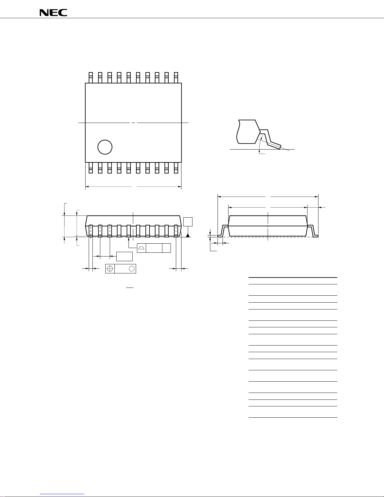
20-pin Plastic shrink SOP (300 mils)
*
20 11
110
A
F
G
µ
PD754144, 754244
detail of lead end
P
H
I
J
S
E
NS
C
M
M
D
NOTE
1. Controlling dimension millimeter.
2. Each lead centerline is located within 0.12 mm (0.005 inch) of
its true position (T.P.) at maximum material condition.
B
L
K
ITEM MILLIMETERS INCHES
6.7±0.3 0.264
A
B
0.575 MAX.
C
0.65 (T.P.)
D
0.32
E
0.125±0.075
2.0 MAX.
F
1.7±0.1
G
8.1±0.3
H
I
6.1±0.2
J
1.0±0.2
K
0.15
L
0.5±0.2
0.12
M
0.10
N
+7°
3° 3°
P
–3°
+0.08
–0.07
+0.10
–0.05
+0.012
–0.013
0.023 MAX.
0.026 (T.P.)
+0.003
0.013
–0.004
0.005±0.003
0.079 MAX.
+0.004
0.067
–0.005
0.319±0.012
0.240±0.008
+0.009
0.039
–0.008
+0.004
0.006
–0.002
+0.008
0.020
–0.009
0.005
0.004
+7°
–3°
P20GM-65-300B-3
Data Sheet U10040EJ2V1DS
77
µ
*
PD754144, 754244
17. RECOMMENDED SOLDERING CONDITIONS
The µPD754144 and µPD754244 should be soldered and mounted under the following recommended
conditions.
For technical information, see the following website.
Semiconductor Device Mount Manual (http://www.necel.com/pkg/en/mount/index.html)
Table 17-1. Surface Mounting Type Soldering Conditions (1/3)
(1)
µ
PD754244GS-xxx-GJG: 20-pin plastic shrink SOP (300 mil, 0.65 mm pitch)
Soldering Method Soldering Conditions Recommended
Condition Symbol
Infrared reflow Package peak temperature: 235°C, Time: 30 seconds max. (at 210°C or higher), IR35-00-2
Count: Twice or less
VPS Package peak temperature: 215°C, Time: 40 seconds max. (at 200°C or higher), VP15-00-2
Count: Twice or less
Wave soldering Solder bath temperature: 260°C max., Time: 10 seconds max., Count: Once WS60-00-1
Preheating temperature: 120°C max. (package surface temperature)
Partial heating Pin temperature: 350°C max., Time: 3 seconds max. (per pin row) –
Caution Do not use different soldering methods together (except for partial heating).
Remark For soldering methods and conditions other than those recommended above, contact an NEC
Electronics sales representative.
(2)
µ
PD754144GS-xxx-GJG: 20-pin plastic shrink SOP (300 mil, 0.65 mm pitch)
Soldering Method Soldering Conditions Recommended
Condition Symbol
Infrared reflow Package peak temperature: 235°C, Time: 30 seconds max. (at 210°C or higher), IR35-00-3
Count: Three times or less
VPS Package peak temperature: 215°C, Time: 40 seconds max. (at 200°C or higher), VP15-00-3
Count: Three times or less
Wave soldering Solder bath temperature: 260°C max., Time: 10 seconds max., Count: Once WS60-00-1
Preheating temperature: 120°C max. (package surface temperature)
Partial heating Pin temperature: 350°C max., Time: 3 seconds max. (per pin row) –
Caution Do not use different soldering methods together (except for partial heating).
Remark For soldering methods and conditions other than those recommended above, contact an NEC
Electronics sales representative.
78 Data Sheet U10040EJ2V1DS
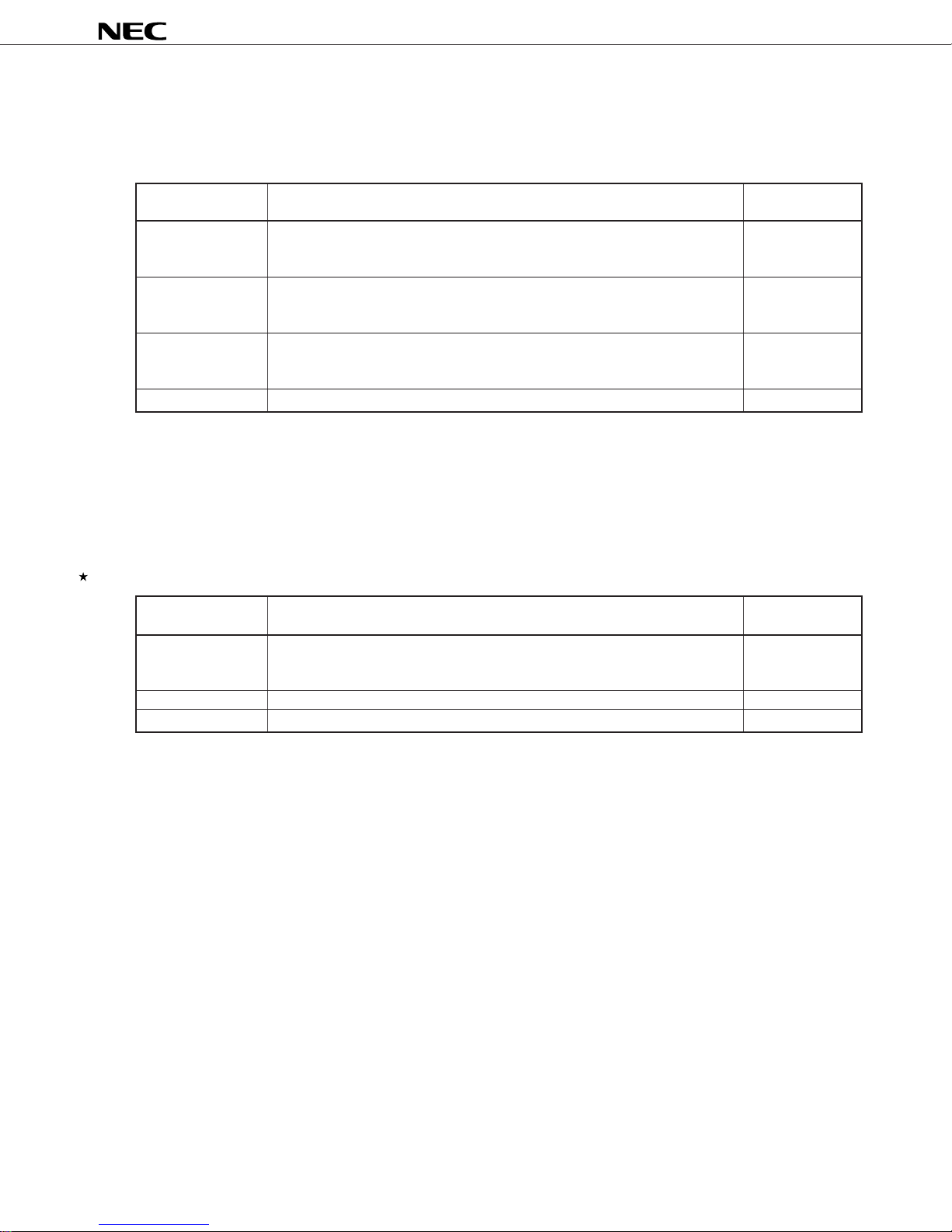
µ
*
PD754144, 754244
Table 17-1. Surface Mounting Type Soldering Conditions (2/3)
(3)
µ
PD754144GS-xxx-BA5: 20-pin plastic SOP (300 mil, 1.27 mm pitch)
µ
PD754244GS-xxx-BA5: 20-pin plastic SOP (300 mil, 1.27 mm pitch)
Soldering Method Soldering Conditions Recommended
Condition Symbol
Infrared reflow Package peak temperature: 235°C, Time: 30 seconds max. (at 210°C or higher), IR35-107-2
Count: Twice or less,
Exposure limit: 7 days
VPS Package peak temperature: 215°C, Time: 40 seconds max. (at 200°C or higher), VP15-107-2
Count: Twice or less,
Exposure limit: 7 days
Wave soldering Solder bath temperature: 260°C max., Time: 10 seconds max., Count: Once WS60-107-1
Preheating temperature: 120°C max. (package surface temperature)
Exposure limit: 7 days
Partial heating Pin temperature: 350°C max., Time: 3 seconds max. (per pin row) –
Note
(after that, prebake at 125°C for 10 to 72 hours)
Note
(after that, prebake at 125°C for 10 to 72 hours)
Note
(after that, prebake at 125°C for 10 to 72 hours)
Note After opening the dry pack, store it at 25°C or less and 65% RH or less for the allowable storage period.
Caution Do not use different soldering methods together (except for partial heating).
Remark For soldering methods and conditions other than those recommended above, contact an NEC
Electronics sales representative.
(4)
µ
PD754244GS-xxx-BA5-A: 20-pin plastic SOP (300 mil, 1.27 mm pitch)
Soldering Method Soldering Conditions Recommended
Condition Symbol
Infrared reflow Package peak temperature: 260°C, Time: 60 seconds max. (at 220°C or higher), IR60-103-3
Count: Three times or less,
Exposure limit: 3 days
Wave soldering For details, contact an NEC Electronics sales representative. –
Partial heating Pin temperature: 350°C max., Time: 3 seconds max. (per pin row) –
Note
(after that, prebake at 125°C for 10 to 72 hours)
Note After opening the dry pack, store it at 25°C or less and 65% RH or less for the allowable storage period.
Caution Do not use different soldering methods together (except for partial heating).
Remarks 1. Products with “-A” at the end of the part number are lead-free products.
2. For soldering methods and conditions other than those recommended above, contact an NEC
Electronics sales representative.
Data Sheet U10040EJ2V1DS
79

Table 17-1. Surface Mounting Type Soldering Conditions (3/3)
*
(5)
µ
PD754144GS-xxx-BA5-A: 20-pin plastic SOP (300 mil, 1.27 mm pitch)
µ
PD754144GS-xxx-GJG-A: 20-pin plastic shrink SOP (300 mil, 0.65 mm pitch)
µ
PD754144GS-xxx-GJG-A: 20-pin plastic shrink SOP (300 mil, 0.65 mm pitch)
Undefined
Remark Products with -A at the end of the part number are lead-free products.
µ
PD754144, 754244
80 Data Sheet U10040EJ2V1DS
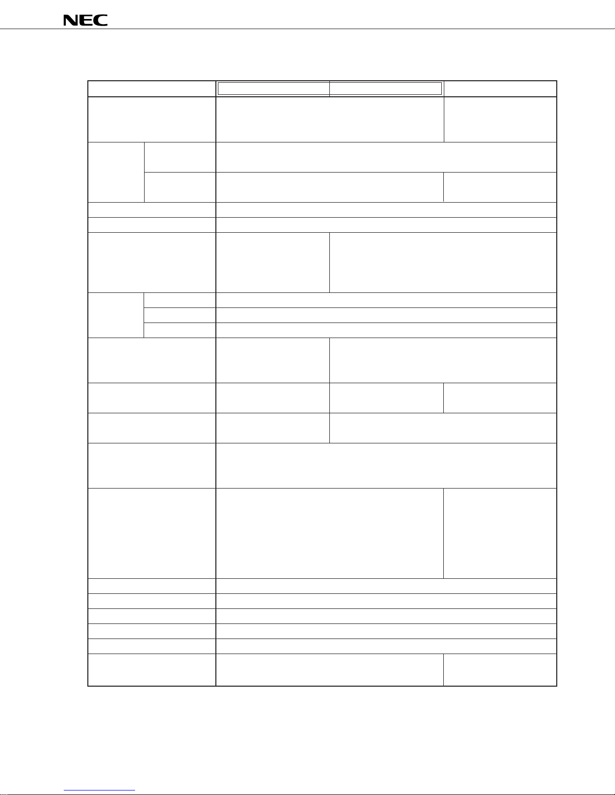
µ
*
PD754144, 754244
APPENDIX A. COMPARISON OF FUNCTIONS AMONG µPD754144, 754244, AND 75F4264
Item
Program memory Mask ROM Flash memory
Data Static RAM 000H to 07FH
memory (128 x 4 bits)
EEPROM 400H to 41FH 400H to 43FH
CPU 75XL CPU
General-purpose register (4 bits x 8 or 8 bits x 4) x 4 banks
Instruction execution time • 4, 8, 16, 64 µs• 0.67, 1.33, 2.67, 10.7 µs
I/O port CMOS input 4 (on-chip pull-up resistor can be connected by mask option)
CMOS I/O 9 (on-chip pull-up resistor connection can be specified by means of software)
Total 13
System clock oscillator RC oscillator Ceramic/crystal oscillator
Start-up time after reset 56/fCC 217/fX, 215/fX (can be 215/fX
Standby mode release time 29/fCC 220/fX, 217/fX, 215/fX, 213/fX
Timer 4 channels
A/D converter None • 8-bit resolution x 2
Programmable threshold port 2 channels
Vectored interrupt External: 1, internal: 5
Test input External: 1 (key return reset function available)
Power supply voltage VDD = 1.8 to 6.0 V
Operating ambient temperature TA = –40 to +85°C
Package • 20-pin plastic SOP (300 mil, 1.27-mm pitch) • 20-pin plastic SOP
µ
PD754144
0000H to 0FFFH 0000H to 0FFFH
(4096 x 8 bits) (4096 x 8 bits)
(16 x 8 bits) (32 x 8 bits)
(@ fCC = 1.0-MHz (@ fX = 6.0-MHz operation)
operation) • 0.95, 1.91, 3.81, 15.3 µs
(resistor and capacitor are
connected externally)
• 8-bit timer counter: 3 channels (can be used as 16-bit timer counter)
• Basic interval timer/watchdog timer: 1 channel
• 20-pin plastic shrink SOP (300 mil, 0.65-mm pitch) (300 mil, 1.27-mm pitch)
µ
PD754244
(@ fX = 4.19-MHz operation)
selected by mask option)
(can be selected by the setting of BTM)
µ
PD75F4264
channels (successive
approximation, hardware
control)
• Can be operated
from VDD = 1.8 V
Note
Note Under development
Data Sheet U10040EJ2V1DS
81
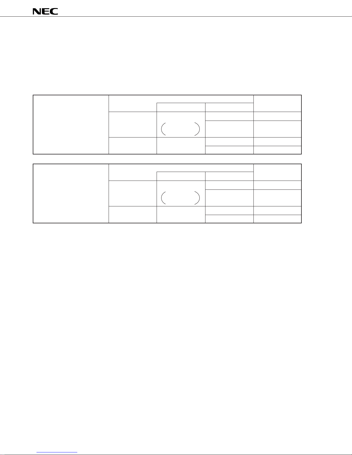
µ
*
PD754144, 754244
APPENDIX B DEVELOPMENT TOOLS
The following development tools are provided for system development using the µPD754244.
In the 75XL series, the relocatable assembler which is common to the series is used in combination with the
device file of each product.
Language processor
RA75X relocatable assembler
Device file
Host machine
PC-9800 series MS-DOS
IBM PC/ATTM and Refer to
compatible machines
Host machine
PC-9800 series MS-DOS 3.5-inch 2HD
IBM PC/AT and Refer to
compatible machines
OS Distribution media
TM
Ver. 3.30 to 5-inch 2HD
Note
Ver. 6.2
“OS for IBM PC”
OS Distribution media
Ver. 3.30 to 5-inch 2HD
Note
Ver. 6,2
“OS for IBM PC”
3.5-inch 2HD
3.5-inch 2HC
5-inch 2HC
3.5-inch 2HC
5-inch 2HC
Part number
(product name)
µ
S5A13RA75X
µ
S5A10RA75X
µ
S7B13RA75X
µ
S7B10RA75X
Part number
(product name)
µ
S5A13DF754244
µ
S5A10DF754244
µ
S7B13DF754244
µ
S7B10DF754244
Note Ver.5.00 or later have the task swap function, but it cannot be used for this software.
Remark Operation of the assembler and device file are guaranteed only on the above host machine and OSs.
82 Data Sheet U10040EJ2V1DS

µ
*
PD754144, 754244
Debugging tool
The in-circuit emulators (IE-75000-R and IE-75001-R) are available as the program debugging tool for the
µ
PD754244.
The system configurations are described as follows.
Hardware IE-75000-R
IE-75001-R In-circuit emulator for debugging the hardware and software when developing applica-
IE-75300-R-EM Emulation board for evaluating the application systems that use the µPD754244.
EP-754144GS-R Emulation probe for the
EV-9500GS-20 SOPs) and EV-9501GS-20 (supporting 20-pin plastic SOPs) which facillitate connection
EV-950IGS-20 to a target system.
Software IE control program Connects the IE-75000-R or IE-75001-R to a host machine via RS-232-C and Centronix
Note 1
In-circuit emulator for debugging the hardware and software when developing application systems that use the 75X series and 75XL series. When developing the
µ
PD754244, the emulation board IE-75300-R-EM and emulation probe EP-754144GS-R
that are sold separately must be used with the IE-75000-R.
By connecting with the host machine, efficient debugging can be made.
It contains the emulation board IE-75000-R-EM which is connected.
tion systems that use the 75X series and 75XL series. When developing the
µ
PD754244, the emulation board IE-75300-R-EM and emulation probe EP-754144GS-R
which are sold separately must be used with the IE-75001-R.
By connecting the host machine, efficient debugging can be made.
It must be used with the IE-75000-R or IE-75001-R.
µ
PD754244GS.
It must be connected to IE-75000-R (or IE-75001-R) and IE-75300-R-EM.
It is supplied with the flexible boards EV-9500GS-20 (supporting 20-pin plastic shrink
I/F and controls the above hardware on a host machine.
Host machine
PC-9800 series MS-DOS 3.5-inch 2HD
IBM PC/AT and its Refer to
compatible machine
“OS for IBM PC”
OS Distribution media
Ver. 3.30 to 5-inch 2HD
Note 2
Ver. 6.2
3.5-inch 2HC
5-inch 2HC
Part No.
(product name)
µ
S5A13IE75X
µ
S5A10IE75X
µ
S7B13IE75X
µ
S7B10IE75X
Notes 1. Maintenance parts
2. Ver.5.00 or later have the task swap function, but it cannot be used for this software.
Remark Operation of the IE control program is guaranteed only on the above host machines and OSs.
Data Sheet U10040EJ2V1DS
83

µ
*
PD754144, 754244
OS for IBM PC
The following IBM PC OS’s are supported.
OS Version
PC DOS
MS-DOS Ver. 5.0 to Ver. 6.22
IBM DOS
TM
Ver. 5.02 to Ver. 6.3
J6.1/V
5.0/V
TM
J5.02/V
Note
to J6.3/V
Note
to J6.2/V
Note
Note
Note
Note Supported only English mode.
Caution Ver. 5.0 and later have the task swap function, but it cannot be used for operating systems
above.
84 Data Sheet U10040EJ2V1DS
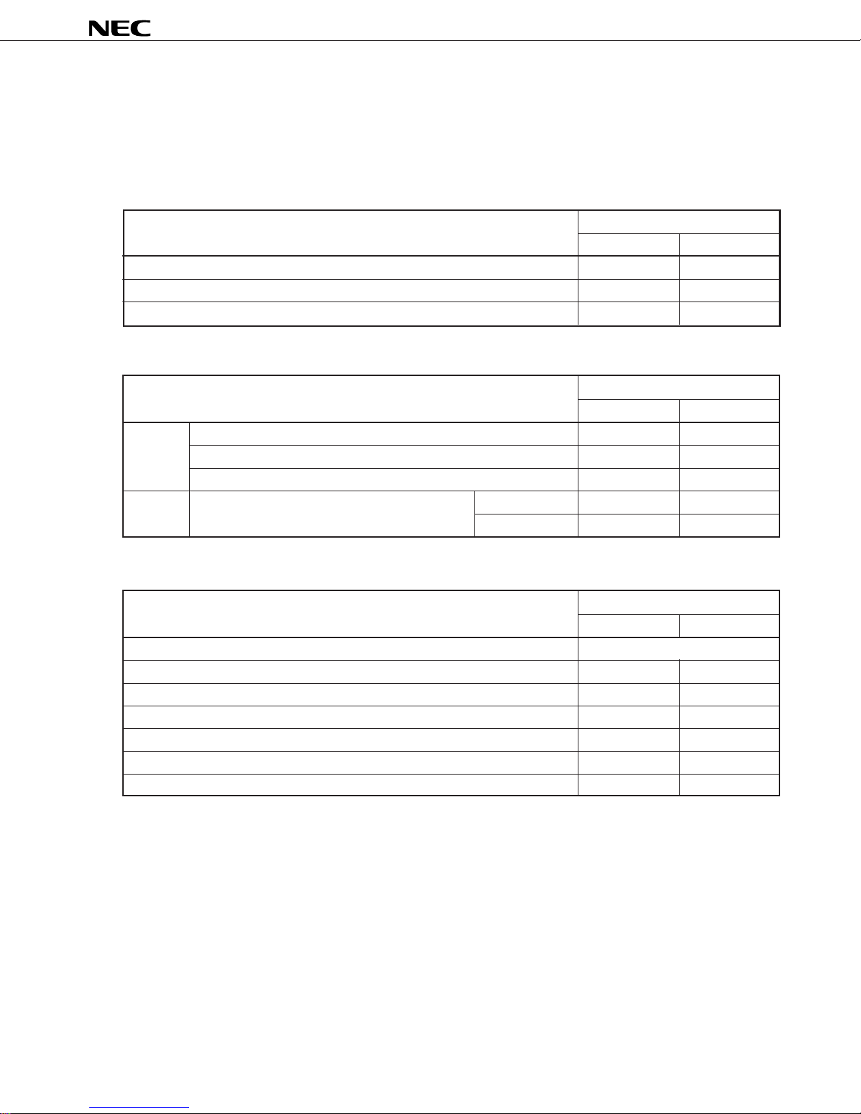
µ
*
PD754144, 754244
APPENDIX C. RELATED DOCUMENTS
The related documents indicated in this publication may include preliminary versions. However, preliminary
versions are not marked as such.
Device related documents
Document Name
µ
PD754144, 754244 Data Sheet U10040J This document
µ
PD754144, 754244 User’s Manual U10676J U10676E
75XL Series Selection Guide U10453J U10453E
Document Number
Japanese English
Development tool related documents
Document Name
Hardware IE-75000-R/IE-75001-R User's Manual EEU-846 EEU-1416
IE-75300-R-EM User's Manual U11354J U11354E
EP-754144GS-R User's Manual U10695J U10695E
Software RA75X Assembler Package User's Manual Operation EEU-731 EEU-1346
Language EEU-730 EEU-1363
Document Number
Japanese English
Other related documents
Document Name
IC Package Manual C10943X
Semiconductor Device Mounting Technology Manual C10535J C10535E
Quality Grades on NEC Semiconductor Devices C11531J C11531E
NEC Semiconductor Device Reliability/Quality Control System C10983J C10983E
Static Electricity Discharge (ESD) Test MEM-539 –
Guide to Quality Assurance for Semiconductor Devices C11893J MEI-1202
Microcomputer Related Product Guide - Other Manufacturers U11416J –
Document Number
Japanese English
Caution These documents are subject to change without notice. Be sure to read the latest documents.
Data Sheet U10040EJ2V1DS
85

µ
*
PD754144, 754244
NOTES FOR CMOS DEVICES
1
VOLTAGE APPLICATION WAVEFORM AT INPUT PIN
Waveform distortion due to input noise or a reflected wave may cause malfunction. If the input of the
IL
CMOS device stays in the area between V
malfunction. Take care to prevent chattering noise from entering the device when the input level is
fixed, and also in the transition period when the input level passes through the area between V
IH
(MIN).
and V
HANDLING OF UNUSED INPUT PINS
2
Unconnected CMOS device inputs can be cause of malfunction. If an input pin is unconnected, it is
possible that an internal input level may be generated due to noise, etc., causing malfunction. CMOS
devices behave differently than Bipolar or NMOS devices. Input levels of CMOS devices must be fixed
high or low by using pull-up or pull-down circuitry. Each unused pin should be connected to V
GND via a resistor if there is a possibility that it will be an output pin. All handling related to unused pins
must be judged separately for each device and according to related specifications governing the device.
3
PRECAUTION AGAINST ESD
A strong electric field, when exposed to a MOS device, can cause destruction of the gate oxide and
ultimately degrade the device operation. Steps must be taken to stop generation of static electricity as
much as possible, and quickly dissipate it when it has occurred. Environmental control must be
adequate. When it is dry, a humidifier should be used. It is recommended to avoid using insulators that
easily build up static electricity. Semiconductor devices must be stored and transported in an anti-static
container, static shielding bag or conductive material. All test and measurement tools including work
benches and floors should be grounded. The operator should be grounded using a wrist strap.
Semiconductor devices must not be touched with bare hands. Similar precautions need to be taken for
PW boards with mounted semiconductor devices.
(MAX) and VIH (MIN) due to noise, etc., the device may
IL
(MAX)
DD
or
4
STATUS BEFORE INITIALIZATION
Power-on does not necessarily define the initial status of a MOS device. Immediately after the power
source is turned ON, devices with reset functions have not yet been initialized. Hence, power-on does
not guarantee output pin levels, I/O settings or contents of registers. A device is not initialized until the
reset signal is received. A reset operation must be executed immediately after power-on for devices
with reset functions.
5
POWER ON/OFF SEQUENCE
In the case of a device that uses different power supplies for the internal operation and external
interface, as a rule, switch on the external power supply after switching on the internal power supply.
When switching the power supply off, as a rule, switch off the external power supply and then the
internal power supply. Use of the reverse power on/off sequences may result in the application of an
overvoltage to the internal elements of the device, causing malfunction and degradation of internal
elements due to the passage of an abnormal current.
The correct power on/off sequence must be judged separately for each device and according to related
specifications governing the device.
6
INPUT OF SIGNAL DURING POWER OFF STATE
Do not input signals or an I/O pull-up power supply while the device is not powered. The current
injection that results from input of such a signal or I/O pull-up power supply may cause malfunction and
the abnormal current that passes in the device at this time may cause degradation of internal elements.
Input of signals during the power off state must be judged separately for each device and according to
related specifications governing the device.
86 Data Sheet U10040EJ2V1DS

µ
*
PD754144, 754244
Regional Information
Some information contained in this document may vary from country to country. Before using any NEC
Electronics product in your application, pIease contact the NEC Electronics office in your country to
obtain a list of authorized representatives and distributors. They will verify:
•
Device availability
•
Ordering information
•
Product release schedule
•
Availability of related technical literature
•
Development environment specifications (for example, specifications for third-party tools and
components, host computers, power plugs, AC supply voltages, and so forth)
•
Network requirements
In addition, trademarks, registered trademarks, export restrictions, and other legal issues may also vary
from country to country.
[GLOBAL SUPPORT]
http://www.necel.com/en/support/support.html
NEC Electronics America, Inc. (U.S.)
Santa Clara, California
Tel: 408-588-6000
800-366-9782
N
EC Electronics (Europe) GmbH
Duesseldorf, Germany
Tel: 0211-65030
•
Sucursal en España
Madrid, Spain
Tel: 091-504 27 87
•
Succursale Française
Vélizy-Villacoublay, France
Tel: 01-30-67 58 00
•
Filiale Italiana
Milano, Italy
Tel: 02-66 75 41
•
Branch The Netherlands
Eindhoven, The Netherlands
Tel: 040-265 40 10
•
Tyskland Filial
Taeby, Sweden
Tel: 08-63 87 200
NEC Electronics Hong Kong Ltd.
Hong Kong
Tel: 2886-9318
NEC Electronics Hong Kong Ltd.
Seoul Branch
Seoul, Korea
Tel: 02-558-3737
NEC Electronics Shanghai Ltd.
Shanghai, P.R. China
Tel: 021-5888-5400
NEC Electronics Taiwan Ltd.
Taipei, Taiwan
Tel: 02-2719-2377
NEC Electronics Singapore Pte. Ltd.
Novena Square, Singapore
Tel: 6253-8311
•
United Kingdom Branch
Milton Keynes, UK
Tel: 01908-691-133
Data Sheet U10040EJ2V1DS
J05.6
87

µ
*
PD754144, 754244
EEPROM is a trademark of NEC Electronics Corporation.
MS-DOS is either a registered trademark or a trademark of Microsoft Corporation in the
United States and/or other countries.
IBM DOS, PC/AT, and PC DOS are trademarks of International Business Machines
Corporation.
These commodities, technology or software, must be exported in accordance
with the export administration regulations of the exporting country.
Diversion contrary to the law of that country is prohibited.
•
The information in this document is current as of August, 2005. The information is subject to
change without notice. For actual design-in, refer to the latest publications of NEC Electronics data
sheets or data books, etc., for the most up-to-date specifications of NEC Electronics products. Not
all products and/or types are available in every country. Please check with an NEC Electronics sales
representative for availability and additional information.
•
No part of this document may be copied or reproduced in any form or by any means without the prior
written consent of NEC Electronics. NEC Electronics assumes no responsibility for any errors that may
appear in this document.
•
NEC Electronics does not assume any liability for infringement of patents, copyrights or other intellectual
property rights of third parties by or arising from the use of NEC Electronics products listed in this document
or any other liability arising from the use of such products. No license, express, implied or otherwise, is
granted under any patents, copyrights or other intellectual property rights of NEC Electronics or others.
Descriptions of circuits, software and other related information in this document are provided for illustrative
•
purposes in semiconductor product operation and application examples. The incorporation of these
circuits, software and information in the design of a customer's equipment shall be done under the full
responsibility of the customer. NEC Electronics assumes no responsibility for any losses incurred by
customers or third parties arising from the use of these circuits, software and information.
•
While NEC Electronics endeavors to enhance the quality, reliability and safety of NEC Electronics products,
customers agree and acknowledge that the possibility of defects thereof cannot be eliminated entirely. To
minimize risks of damage to property or injury (including death) to persons arising from defects in NEC
Electronics products, customers must incorporate sufficient safety measures in their design, such as
redundancy, fire-containment and anti-failure features.
•
NEC Electronics products are classified into the following three quality grades: "Standard", "Special" and
"Specific".
The "Specific" quality grade applies only to NEC Electronics products developed based on a customerdesignated "quality assurance program" for a specific application. The recommended applications of an NEC
Electronics product depend on its quality grade, as indicated below. Customers must check the quality grade of
each NEC Electronics product before using it in a particular application.
"Standard":
"Special":
"Specific":
Computers, office equipment, communications equipment, test and measurement equipment, audio
and visual equipment, home electronic appliances, machine tools, personal electronic equipment
and industrial robots.
Transportation equipment (automobiles, trains, ships, etc.), traffic control systems, anti-disaster
systems, anti-crime systems, safety equipment and medical equipment (not specifically designed
for life support).
Aircraft, aerospace equipment, submersible repeaters, nuclear reactor control systems, life
support systems and medical equipment for life support, etc.
The quality grade of NEC Electronics products is "Standard" unless otherwise expressly specified in NEC
Electronics data sheets or data books, etc. If customers wish to use NEC Electronics products in applications
not intended by NEC Electronics, they must contact an NEC Electronics sales representative in advance to
determine NEC Electronics' willingness to support a given application.
(Note)
(1)
"NEC Electronics" as used in this statement means NEC Electronics Corporation and also includes its
majority-owned subsidiaries.
(2)
"NEC Electronics products" means any product developed or manufactured by or for NEC Electronics (as
defined above).
M8E 02. 11-1
 Loading...