


September, 2002
NEC Corporation
Service manual
59/68 Cm STEREO Color Television
MODEL : DTE-25G5THS
DTE-29G5TH
FS-59T90
FS-68T90
DTE-25G4ZH
DTE-29G4ZH
FS-59V81
FS-68V81
CHASSIS : CP-785A
S/M No. : TCP785AEFR1

Contents
1 - Main features
2
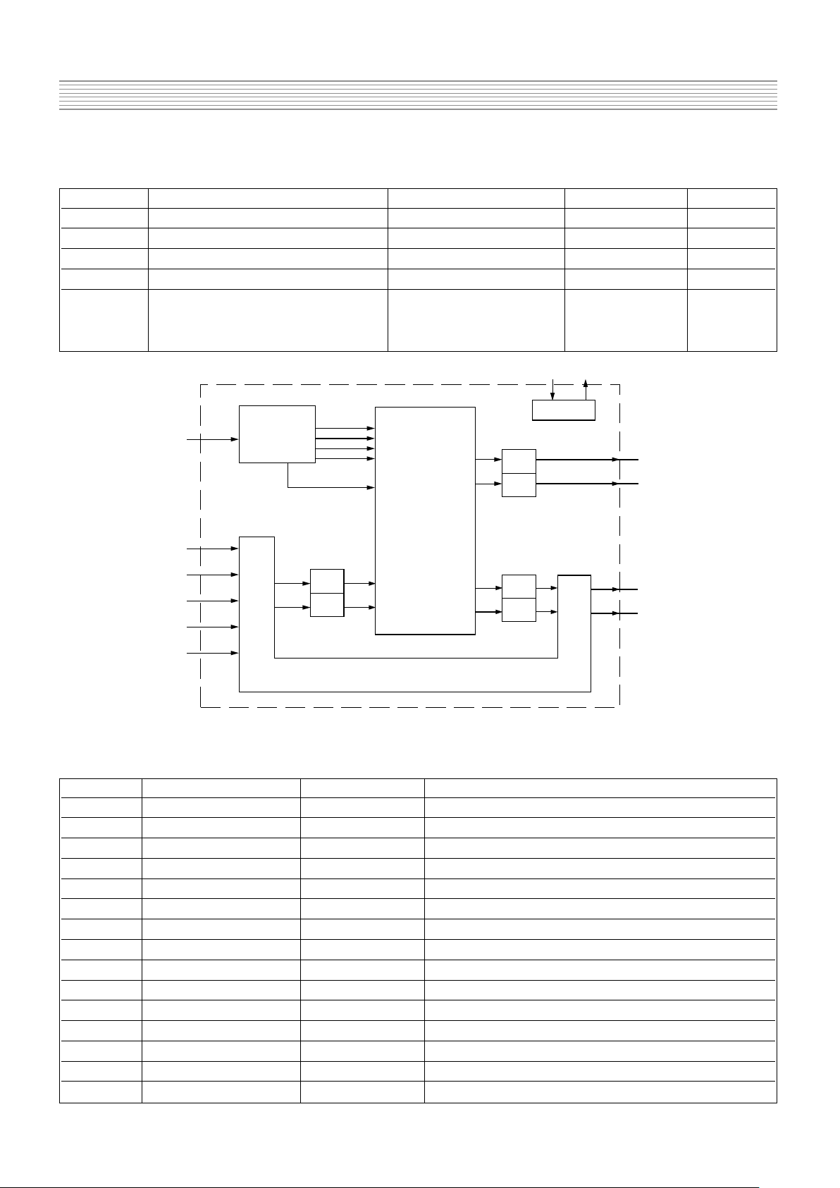
1-1 Specifications
2
1-2 External Terminals
2
1-3 Channel table
4
2 - Safety instruction
7
3 - Alignment instructions
8
3-1 Microcontroller configuration : Service mode
8
3-2 Microcnotroller configuration : Option
8
3-3 TV set Alignment
10
4 - IC description
12
4-1 TDA936x TV signal processor - TXT with embedded
-Controller 12
4-2 MSP34 Multistandard Sound Processor
19
4-3 TDA894x J Stereo Audio Amplifier
23
4-4 TDA835x J Vertical Amplifier
24
4-5 TDA6107Q
26
4-6 24C08 8 K bit EEPROM
27
4-7 STR-F665X
28
5 - Circuit description
30
5-1 Block diagram
30
5-2 IF
34
5-3 Source switching
35
5-4
-Controller I/O pin configuration and function 35
5-5 Sound processing
36
5-6 Sound amplification
37
5-7 Vertical deflection
38
5-8 Power supply (STR-F6654)
39
5-9 TV start-up, TV normal run and stand by mode operations
43
6 - Service parts list
50
6-1 PCB Difference Part (PCB change of FS-xxT90)
51
6-2 CRT Difference Part
59
6-3 Function & Cabinet Difference Part
60
6-4 All Electrical Parts List
61
7 - Compaitible Components List for FS-xxT90, xxV81
8 - Exploded view 83
9 - PCB Layout
84
9-1 Old Main PCB (4859804393)
85
9-2 New Main PCB (4859806493)
86
9-3 Control PCB (4859833214)
87
10 - Circuit Diagram
88
10-1 Old Main PCB 88
10-2 New Main PCB & Control PCB
89
-1--1-

-2-
Service Manual CP-785A
1-1 Specifications
1-2 External Teminals
1-2-1 Input 2 : Rear RCA
TV standard PAL, - B/G, H
Sound system NICAM B/G
FM 2Carrier B/G
Power consumption 25” : 113W approx.
29” : 118W approx.
Sound Output Power 25” : 5W x 5W (at 60% mod, 10% THD)
29” : 5W x 5W (at 60% mod, 10% THD)
Speaker 25” : 7W 8 ohm x 2
29” : 7W 8 ohm x 2
Teletext system 10 pages memory FASTEXT (FLOF or TOP) : Option
Aerial input 75 ohm unbalanced
Channel coverage Off-air channels, S-cable channels and hyperband
Tuning system frequency synthesiser tuning system
Visual screen size 25” : 59 Cm
29” : 68 Cm
Channel indicatio On Screen Display
Program Selection 100 programmes
Aux. terminal INPUT1(SCART or RCA)
- SCART : Audio / Video In, S-VHS In(with cable)
- RCA : Audio / Video In. (SVHS : disable)
INPUT2(RCA) : Audio / Video In
OUTPUT(RCA) : TV OUT
Headphone jack (3.5 mm) on front of cabinet
Remote Control Unit R-44N08(RD-D90) for with Teletext
R-44N09(RD-085) for with Teletext
Pin Signal Matching value
1(Yellow) Video Input 1.0 Vpp+/- 3dB, Impedance 75 ohm
2(White) Audio Input Left 0.5 Vrms, Impedance > 10k ohm
3(Red) Audio Input Right 0.5 Vrms, Impedance > 10k ohm
1-2-2 Output : Rear RCA
Pin Signal Matching value
1(Yellow) TV Video 1.0 Vpp+/- 3dB, Impedance 75 ohm
2(White) TV Audio Left 0.5 Vrms at RF Sound FM 54%Mod.(27kHz dev.)
3(Red) TV Audio Right 0.5 Vrms at RF Sound FM 54%Mod.(27kHz dev.)
1-2-3 Input1 : Rear RCA or Scart
-RCA Jack : Input1 (S-VHS not available)
Pin Signal Matching value
1(Yellow) Video Input 1.0 Vpp+/- 3dB, Impedance 75 ohm
2(White) Audio Input Left 0.5 Vrms, Impedance > 10k ohm
3(Red) Audio Input Right 0.5 Vrms, Impedance > 10k ohm
-2-
-3-
Service Manual CP-785A
- SCART (21pin Euro Scart) : Input1 & S-VHS input
Pin Signal Matching value
1 N.C.
2 Audio Input Right 0.5 Vrms, Impedance > 10 kΩ
3 N.C.
4 Audio Earth
5 Earth
6 Audio Input Left 0.5 Vrms, Impedance > 10 kΩ
7 N.C.
8 N.C.
9 N.C.
10 N.C.
11 N.C.
12 N.C.
13 N.C.
14 Earth
15 Chroma Input +/- 3dB for a luminance signal of 1 Vpp
16 N.C.
17 Earth
18 Video In Earth
19 N.C.
20 Video Input / Y Input 1 Vpp +/- 3dB, Impedance 75 ohm
21 Common Earth
-4-
Service Manual CP-785A
1-3 Channel table
FREQUENCY TABLE CP-785A
CH AUSTRALIA N/Z˅land
C00 46.25
C01 57.25
C02 64.25
C03 86.25
C04 95.25
C05 102.25
C5A 138.25
C06 175.25
C07 182.25
C08 189.25
C09 196.25
C10 209.25
C11 216.75
N01 - 45.25
N02 - 55.25
N03 - 62.25
N08 - 203.25
N09 - 210.25
N10 - 217.25
- - C21 471.25
C22 479.25
C23 487.25
C24 495.25
C25 503.25
C26 511.25
C27 519.25
C28 527.25
C29 534.25
C30 541.25
C31 548.25
C32 555.25
C33 562.25
C34 569.25
C35 576.25
C36 583.25
C37 590.25
C38 597.25
C39 603.25
C40 610.25
C41 617.25
C42 624.25

-5-
Service Manual CP-785A
CH AUSTRALIA N/Z˅land
C43 631.25
C44 638.25
C45 645.25
C46 652.25
C47 659.25
C48 666.25
C49 673.25
C50 680.25
C51 687.25
C52 694.25
C53 701.25
C54 708.25
C55 715.25
C56 722.25
C57 729.25
C58 736.25
C59 743.25
C60 750.25
C61 757.25
C62 764.25
C63 771.25
C64 779.25
C65 786.25
C66 793.25
C67 800.25
C68 807.25
C69 814.25
C70 C71 C72 C73 C74 C75 C76 C77 S01 105.25
S02 112.25
S03 119.25
S04 126.25
S05 133.25
S06 140.25
S07 147.25
S08 154.25
S09 161.25
S10 168.25
S11 231.25
-6-
Service Manual CP-785A
CH AUSTRALIA N/Z˅land
S12 238.25
S13 245.25
S14 252.25
S15 259.25
S16 266.25
S17 273.25
S18 280.25
S19 287.25
S20 294.25
S21 303.25
S22 311.25
S23 319.25
S24 327.25
S25 335.25
S26 343.25
S27 351.25
S28 359.25
S29 367.25
S30 375.25
S31 383.25
S32 391.25
S33 399.25
S34 407.25
S35 415.25
S36 423.25
S37 431.25
S38 439.25
S39 447.25
S40 455.25
S41 463.25

-7-
Service Manual CP-785A
2 - Safety instruction
WARNING: Only competent service personnel may carry out work involving the testing or repair of this
equipment.
X-RAY RADIATION PRECAUTION
1. Excessive high voltage can produce potentially hazardous X-RAY RADIATION. To avoid such
hazards, the high voltage must not exceed the specified limit. The nominal value of the high voltage of
this receiver is 26~28 KV (25” - 29”) at max beam current. The high voltage must not under any
circumstances, exceed 29.5 KV (25") or 31 KV (29"). Each time a receiver requires servicing, the
high voltage should be checked. It is important to use an accurate and reliable high voltage meter.
2.The only source of X-ray Radiation in this TV receiver is the picture tube. For continued X-ray
RADIATION protection, the replacement tube must be exactly the same type tube as specified in the
parts list.
SAFETY PRECAUTION
1. Potentials of high voltage are present when this receiver is operating. Operation of the receiver outside
the cabinet or with the back board removed involves a shock hazard from the receiver.
1) Servicing should not be attempted by anyone who is not thoroughly familiar with the precautions
necessary when working on high voltage equipment.
2) Discharge the high potential of the picture tube before handling the tube. The picture tube is highly
evacuated and if broken, glass fragments will be violently expelled.
2. If any Fuse in this TV receiver is blown, replace it with the FUSE specified in the Replacement Parts
List.
3. When replacing a high wattage resistor (oxide metal film resistor) in circuit board, keep the resistor 10
mm away from circuit board.
4. Keep wires away from high voltage or high temperature components.
5. This receiver must operate under AC 240 volts, 5O Hz. NEVER connect to DC supply or any other
power or frequency.
PRODUCT SAFETY NOTICE
Many electrical and mechanical parts in this equipment have special safety-related characteristics. These
characteristics are often passed unnoticed by a visual inspection and the X-ray Radiation protection
afforded by them cannot necessarily be obtained by using replacement components rated for higher
voltage, wattage, etc. Replacement parts which have these special safety characteristics are identified in
this manual and its supplements, electrical components having such features are identified by designated
symbol on the parts list. Before replacing any of these components, read the parts list in this manual
carefully. The use of substitutes replacement parts which do not have the same safety characteristics as
specified in the parts list may create X-ray Radiation.
-8-
Service Manual CP-785A
3 - Alignment instructions
3-1 Microcontroller configuration : Service mode
To switch the TV set into service mode please see instruction below.
1 - Select pr. number 91
2 - Adjust sharpness to minimum value and exit all menu.
3 - Quickly press the key sequence : RED - GREEN - menu
To exit SERVICE menu press menu key or Operate(Std By) key.
In Service Mode press “OK” to stop the microcontroller i.e. the I2C bus is free and the set can be controlled by
external equipment. Press “OK” again to allow the microcontroller to control the set again.
3-2 Microcontroller configuration : Option
Section Items BareDATA
29
ˉ
25
ˉ
21
ˉ
REMARK
G5TH G4ZH G5THS G4ZH
AGC 32 38 38 38 38 38
BIAS R/G 31/31 31/31 31/31 31/31 31/31 31/31 old micom : 8/8
DRIVE R/G/B 32/32/32 32/32/28 32/32/28 32/32/32 32/32/32 32/32/32
H-PARALLEL 31 36 36 32 32 32
H-BOW 42 34 34 35 35 35
For H-SHIFT 25 30 30 30 30 27
Adjustment V-SLOPE 32 35 35 35 35 35
(Variable) V-Amplitude 39 19 19 30 30 27
V. S-Correction 13 27 27 25 25 23
V SHIFT 32 34 34 34 34 45
H-WIDTH 32 37 37 57 57 33
EW Parabola 32 20 20 17 17 0
Up-Conner 32 32 32 42 42 32
Dn-Conner 32 32 32 42 42 32
EW Trapezium 32 29 29 31 31 29
Option 04 04 04 04 04 04
0,1,2,3 : For D/W Remote controller
4,5,6,7 : For NEC Remote controller
ˉ
CH Lock
or OFF OFF OFF OFF OFF OFF “Hotel Lock” will be changed to “CH Lock”
HOTEL Lock
HOTEL Max Vol
For or 15 43 43 43 43 43 “
Hotel Max Vol” will be changed to “Max Vol”
Function Max VOL
Change
Colck Pr. 01 07 07 07 07 07
change the reference channel
(OPTION) for Automatic clock setting
SVHS ON ON OFF ON OFF OFF OFF : disable S-VHS Input
AV START OFF OFF OFF OFF OFF OFF “AV START” is add
KEY LOCK OFF OFF OFF OFF OFF OFF “KEY LOCK” is add
SCREEN 24 31 31 33 33 35 each CRT has different Adjusting point
-9-
Service Manual CP-785A
Lock Function Name Description
Applied CPU
Remark
Models Version
- Channel Setting : Enable / Disable
Current - Volume Limit (Hotel Max Vol) : Enable / Disable FS-59T90 These current Lock fuction
Lock - When this function is active, It is impossible to change FS-68T90 DW9365-CH1 will be change to New Lock Fuction.
Function Hotel Lock ON / OFF the channel data (can not enter the INSTALL menu) & PF51T31
the sound can be limited by
ˈ
Hotel Max Vol
ˉ
.
- This Function is available When
ˈ
Hotel Lock
ˉ
is on
Hotel (This function is depend on Hotel Lock Function)
Max. Volume 00 ~ 43(max.) - When Hotel Lock is off , the sound dose not limited.
- Channel Setting : Impossible / Possible - Each Lock Function is independence
CH Lock ON / OFF - The former
ˈ
Hotel mode
ˉ
has been removed and added
ˈ
CH lock
ˉ
- It is possible to change the features by
- When this function is active, It is impossible to change combination of each function
New the channel data (can not enter the INSTALL menu) FS-59V81 - We will apply these new lock fuction to
Lock - Max Volume is limited. FS-68V81 current TEXT micom.
Function - Even if
ˈ
CH lock
ˉ
is not active the sound can be DW9365-CH2
Max Vol 00 ~ 43(max.) limited by the service function
ˈ
Max Vol
ˉ
. (FS-59T90) DW9385-CH1 - Examlpe)
- In case of virgin EEPROM, the default setting is 43 (Max). (FS-68T90) CH lock=ON, Max Vol=20
- In normal, the
ˈ
Max. Vol.
ˉ
must be 43 (PF51T31) ==> CH setting = Disable
- When
ˈ
VA start
ˉ
is active, the set always start in AV1 mode Volume Limit : under 20
AV Start ON / OFF (main AC switch on/off & remote controller on/off). Max. Vol=20, AV start=ON, Key Lock=ON
- In case of virgin EEPROM, the default setting is OFF. ==> Volume Limit : under 20
Key Lock ON / OFF - When active the local keyboard cannot be used. Tv is always turn on at AV1 mode
- In case of virgin EEPROM, the default setting is OFF. Front local keys are not operate
Change of Lock Function
(1) Model
- New AV Stereo Model (FS-xxV81, DTE-xxG4ZH) will be applied the new lock function from 1st MP.
- Current Model (FS-xxT90, DTE-xxG5THx) will be changed to new lock function when the CPU software is changed (TDA9365 : DW9365-CH1 ==> DW9365-CH2)
(2) Details
* Note : These Function is changed only Service Mode not Factory mode. So you must use the user
˅
s remote controller
- Change the PR. No. to 91 ==> change the sharpness to 00(min) in Picture control Menu ==> Exit the User control Menu ==> Press the [RED],[GREEN],[MENU] quickly
- Then the Service Menu is appeared.
-10-
Service Manual CP-785A
3-3 TV set Alignment
3-3-1 - G2 alignment
- TV in AV mode without video signal Black screen.
- TV preset with WP Red, WP Green and WP Blue equal to 32.
- TV preset with Black R, Black G equal to 32.
- Set TV in NORMAL I mode
- Adjust screen volume ( on FBT ) such that the highest cathod cut-off voltage measured on CRT
board, is V cut off
5V.
Screen size Vcut-off
25” 140V
29” 140V
3-3-2 - White balance
- Select a dark picture and adjust Black G and Black R to the desired colour temperature.
- Select a bright picture and adjust WP Red, WP Green, WP Blue to the desired colour temperature.
3-3-3 - Focus
- Adjust the Focus volume ( on FBT ) to have the best resolution on screen.
3-3-4 - Vertical geometry
- Adjust the Vertical Amplitude, Shift, S-
Correction and Slope to compensate for vertical
distortion.
3-3-5 - Horizontal picture centering
- Adjust H Shift to have the picture in the center of the screen.
3-3-6 - East / West correction
- Adjust the H Parall, H Bow, H Width, EW Parabo, Up Corner, Dw Corner, EW trapez to compensate
for geometrical distortion.
H. Parall EW.Parabola
-11-
Service Manual CP-785A
3-3-7 - AGC
- Adjust the antenna signal level at 68 dBV 2 (UHF - CH25)
- Set RF AGC to 0.
- Increase RF AGC level and stop when the level on pin 6 of TDA936x goes below 2.5 Vdc
H. Bow
H.Width
Up Corner
Dw Corner
-12-
Service Manual CP-785A
4 - IC description
4-1 TDA936x TV signal processor - Teletext decoder with embedded -Controller.
- TDA936x : TEXT Available
- TDA938x : TEXT Not Available
CHASSIS(MODELS) IC MARKING TEXT TV STANDARD Version History
CP-785A, AF TDA9365 10 PAGE TEXT TDA-9365/N1(otp)
(DTE-xxxxTHx) (DW9365/N2-CH1) (Pan-Eur opeun) PLA/SECAM TDA9365/N2-H:DW9365-CH(Masking)
(FS-XXT90,PF-51T31) TDA9365/N2-I : DW9365-CH2(Masking)
CP-785A TDA9385
(DTE-xxxxZH) -OTP : TDA9385/N2/I Not USED PAL TDA9385/N2-I : DW9385-CH1
(FS-xxV81) -Marsking : TDA9385/N2/I
DW9385/N2/-I-CH1
TV-signal Processor
Multi-standard vision IF circuit with alignment-free PLL demodulator
Internal (switchable) time-constant for the IF-AGC circuit
Source selection between 'Internal' CVBS and external CVBS or Y/C signals
Integrated chrominance trap circuit
Integrated luminance delay line with adjustable delay time
Asymmetrical ‘ delay line type’ peaking in the luminance channel
Black stretching for non-standard luminance signals
lntegrated chroma band-pass filter with switchable centre frequency
Only one reference (12 MHz) crystal required for the -Controller, Teletext and the colour decoder
PAL / NTSC or multistandard colour decoder with automatic search system
Internal base-band delay line
RGB control circuit with 'Continuous Cathode Calibration', white point and black level off set
adjustment so that the colour temperature of the dark and the bright parts of the screen can be chosen
independently.
The Text/OSD signals are internally supplied from the -Controller/Teletext decoder
Contrast reduction possibility during mixed-mode of OSD and Text signals
Horizontal synchronisation with two control loops and alignment-free horizontal oscillator
Vertical count-down circuit
Vertical driver optimised for DC-coupled vertical output stages
Horizontal and vertical geometry processing
Horizontal and vertical zoom function for 16 : 9 applications
Horizontal parallelogram and bow correction for large screen picture tubes

-13-
Service Manual CP-785A
-Controller
80C51 -controller core standard instruction set and timing
1 s machine cycle
32 - 128Kx8-bit late programmed ROM
3 - 12Kx8-bit Auxiliary RAM (shared with Display and Acquisition)
Interrupt controller for individual enable/disable with two level priority
Two 16-bit Timer/Counter registers
WatchDog timer
Auxiliary RAM page pointer
16-bit Data pointer
IDLE and Power Down (PD) mode
14 bits PWM for Voltage Synthesis Tuning
8-bit A/D converter
4 pins which can be programmed as general I/0 pin, ADC input or PWM (6-bit) output
Data Capture
Text memory 10 pages
Inventory of transmitted Teletext pages stored in the Transmitted Page Table (TPT) and Subtitle Page
Table (SPT)
Data Capture for US Closed Caption
Data Capture for 525/625 line WST, VPS (PDC system A) and Wide Screen Signalling (WSS) bit
decoding Automatic selection between 525 WST/625 WST
Automatic selection between 625 WST/VPS on line 16 of VBI
Real-time capture and decoding for WST Teletext in Hardware, to enable optimised -processor
throughput
Automatic detection of FASTEXT transmission
Real-time packet 26 engine in Hardware for processing accented, G2 and G3 characters
Signal quality detector for video and WST/VPS data types
Comprehensive teletext language coverage
Full Field and Vertical Blanking lnterval (VBI) data capture of WST data
Display
Teletext and Enhanced OSD modes
Features of lever 1.5 WST and US Close Caption
Serial and Parallel Display Attributes
Single/Double/Quadruple Width and Height for characters
Scrolling of display region
Variable flash rate controlled by software
Enhanced display features including overlining, underlining and italics
Soft colours using CLUT with 4096 colour palette
Globally selectable scan lines per row (9/10/13/16) and character matrix [12x10, 12xl3, 12x16 (VxH)]
Fringing (Shadow) selectable from N-S-E-W direction
Fringe colour selectable
Meshing of defined area

-14-
Service Manual CP-785A
Contrast reduction of defined area
Cursor
Special Graphics Characters with two planes, allowing four colours per character
32 software redefinable On-Screen display characters
4 WST Character sets (GO/G2) in single device (e.g. Latin, Cyrillic, Greek, Arabic)
G1 Mosaic graphics, Limited G3 Line drawing characters
WST Character sets and Closed Caption Character set in single device
Data Capture
The Data Capture section takes in the analogue Composite Vidéo and Blanking Signal (CVBS), and from
this extracts the required data, which is then decoded and stored in memory.
The extraction of the data is performed in the digital domain. The first stage is to convert the analogue
CVBS signal into a digital form. This is done using an ADC sampling at 12MHz. The data and clock
recovery is then performed by a Multi-Rate Video Input Processor (MuIVIP). From the recovered data
and clock the following data types are extracted WST Teletext (625/525), Closed Caption, VPS, WSS.
The extracted data is stored in either memory (DRAM) via the Memory Interface or in SFR locations.
Data Capture Features
- Video Signal Quality detector
- Data Capture for 625 line WST
- Data Capture for 525 line WST
- Data Capture for US Closed Caption
- Data Capture for VPS data (PDC system A)
- Data Capture for Wide Screen Signalling (WSS) bit decoding
- Automatic selection between 525 WST/625WST
- Automatic selection between 625WST/VPS on line 16 of VBI
- Real-time capture and decoding for WST Teletext in Hardware, to enable optimised microprocessor
throughput
- 10 pages stored On-Chip
- lnventory of transmitted Teletext pages stored in the Transmitted Page Table (TPT) and Subtitle Page
Table (SPT)
- Automatic detection of FASTEXT transmission
- Real-time packet 26 engine in Hardware for processing accented, G2 and G3 characters
- Signal quality detector for WST/VPS data types
- Comprehensive Teletext language coverage
- Full Field and Vertical Blanking Interval (VBI) data capture of WST data
-15-
Service Manual CP-785A
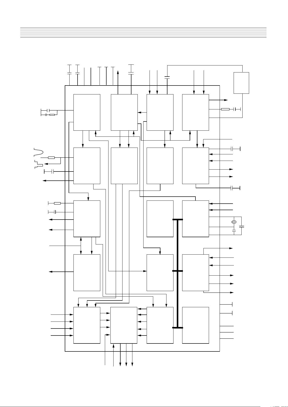
+8V
13
43
24
23
42
40
CVBS/Y
IFIN
TUNERAGC
SOUND
TRAP
27 37
VIDEO SWITCH
VIDEO IDENT.
VIDEO FILTERS
38
(35) (35)
(32)
28 29 44 31 60 55 59 58 57 2 3 4 9 12
10 PAGE
MEMORY
TELETEXT/OSD
DISPLAY
+3.3V
5654 61
(20)
AUDEXT
SIFIN
QSSOUT/AMOUT
AMOUT
RESET
VPE
LED OUT (2x)
VST OUT
ADC IN (4x)
I/O PORTS (4x)
1+62-64
SCL SDA
5-8
10/11
VISION IF
ALIGNMENT-FREE
PLL DEMOD.
AGC/AFC
VIDEO AMP.
CHROMA
PAL/SECAM/NTSC
DECODER
H/V SYNC SEP.
H-OSC. + PLL
(32)
30
41
18
39
14
19
17
H
34 16 33 25 26 22 21 36
(20) 46 47 48 45
50
49
53
52
51
BLKIN
BCLIN
BO
GO
RO
COR
CONTR/BRIGHTN
OSD/TEXT INSERT
CCC
WHITE-P. ADJ.
HOUT
V-DRIVE
EHTO
EWD
R/V
Y
R
R
V
H
G
G
B
B
BL
RGB/YUV INSERT
RGB/YUV MATRIX
SATURATION
YUV/RGB MATRIX
U
V
G/Y
B/U
BL
V
V-DRIVE +
GEOMETRY
ROM/RAM
CVBS
I
2
C-BUS
TRANSCEIVER
VST PWM-DAC
I/O PROTS
TELETEXT
ACQUISITION
SYNC
EW GEOMETRY
H-DRIVE
2
nd
LOOP
H-SHIFT
BASE-BAND
DELAY LINE
REF
REF
QSS SOUND IF
AGC
QSS MIXER
AM DEMODULTOR
ENIANCED
80C51 CPU
LUMA DELAY
PEAKING
BLACK STRETCH
-16-
Service Manual CP-785A
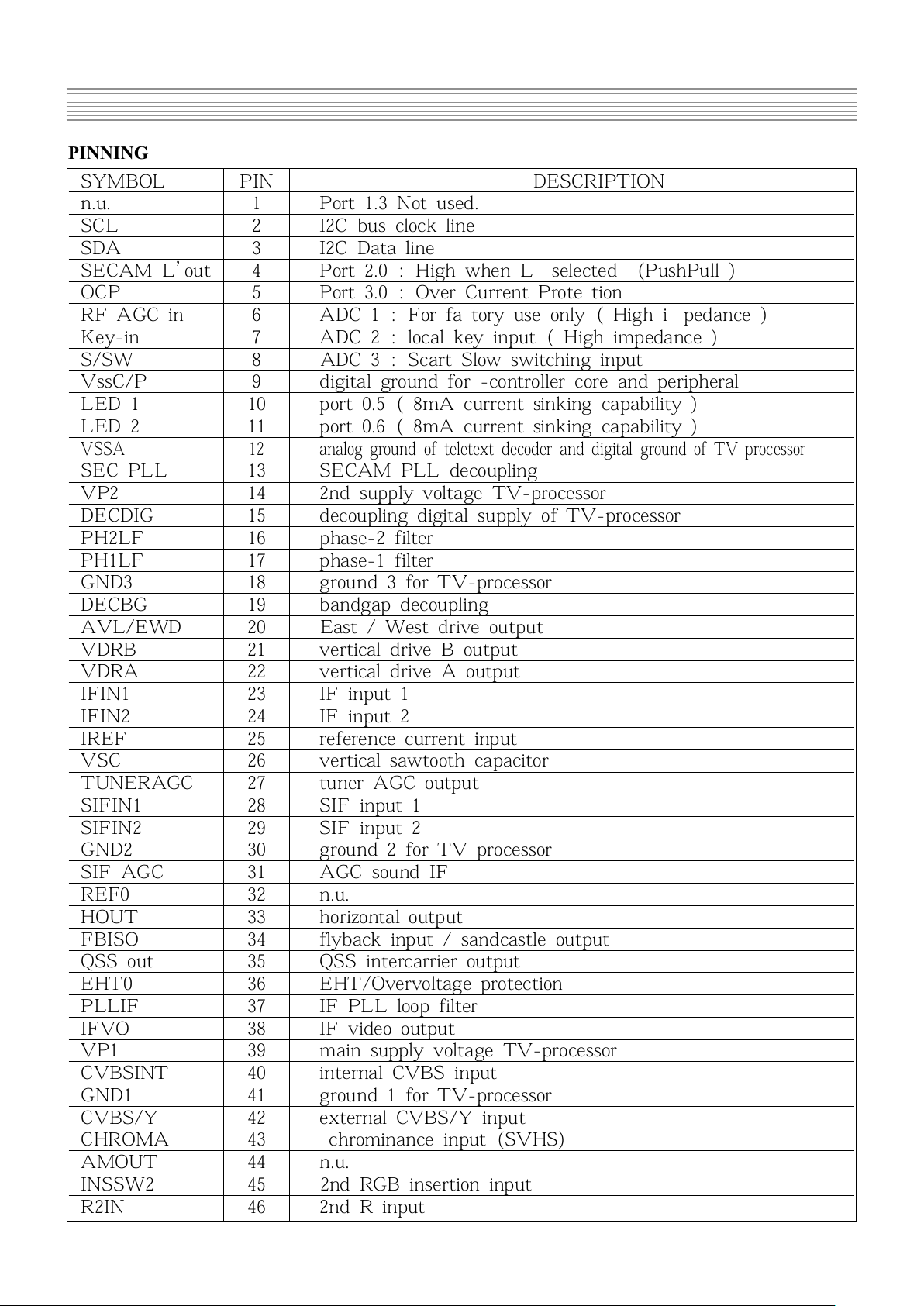
SYMBOL PIN DESCRIPTION
n.u. 1 Port 1.3 Not used.
SCL 2 I2C bus clock line
SDA 3 I2C Data line
SECAM L˅out 4 Port 2.0 : High when Lㅤselected (PushPull )
OCP 5 Port 3.0 : Over Current Protection
RF AGC in 6 ADC 1 : For factory use only ( High impedance )
Key-in 7 ADC 2 : local key input ( High impedance )
S/SW 8 ADC 3 : Scart Slow switching input
VssC/P 9 digital ground for -controller core and peripheral
LED 1 10 port 0.5 ( 8mA current sinking capability )
LED 2 11 port 0.6 ( 8mA current sinking capability )
VSSA 12 analog ground of teletext decoder and digital ground of TV processor
SEC PLL 13 SECAM PLL decoupling
VP2 14 2nd supply voltage TV-processor
DECDIG 15 decoupling digital supply of TV-processor
PH2LF 16 phase-2 filter
PH1LF 17 phase-1 filter
GND3 18 ground 3 for TV-processor
DECBG 19 bandgap decoupling
AVL/EWD 20 East / West drive output
VDRB 21 vertical drive B output
VDRA 22 vertical drive A output
IFIN1 23 IF input 1
IFIN2 24 IF input 2
IREF 25 reference current input
VSC 26 vertical sawtooth capacitor
TUNERAGC 27 tuner AGC output
SIFIN1 28 SIF input 1
SIFIN2 29 SIF input 2
GND2 30 ground 2 for TV processor
SIF AGC 31 AGC sound IF
REF0 32 n.u.
HOUT 33 horizontal output
FBISO 34 flyback input / sandcastle output
QSS out 35 QSS intercarrier output
EHT0 36 EHT/Overvoltage protection
PLLIF 37 IF PLL loop filter
IFVO 38 IF video output
VP1 39 main supply voltage TV-processor
CVBSINT 40 internal CVBS input
GND1 41 ground 1 for TV-processor
CVBS/Y 42 external CVBS/Y input
CHROMA 43 chrominance input (SVHS)
AMOUT 44 n.u.
INSSW2 45 2nd RGB insertion input
R2IN 46 2nd R input
PINNING
-17-
Service Manual CP-785A
SYMBOL PIN DESCRIPTION
G2IN 47 2nd G input
B2IN 48 2nd B input
BCLIN 49 beam current limiter input
BLKIN 50 black current input
R0 51 RED Output
G0 52 GREEN Output
B0 53 BLUE Output
VDDA 54
analog supply of Teletext decoder and digital supply of TV-Processor (3.3V)
VPE 55 OTP programming supply
VDDC 56 digital supply to core (3.3V)
OSCGND 57 oscillator ground supply
XTALIN 58 crystal oscillator input
XTALOUT 59 crystal oscillator output
RESET 60 reset
VDDP 61 digital supply to periphery (3.3V)
Audio Mute 62 Port 1.0 : Audio mute output (PushPull )
Power 63 Port 1.1 : Power output (PushPull )
IR in 64 Interrupt input 0 : R/C Infrared input
-18-
Service Manual CP-785A
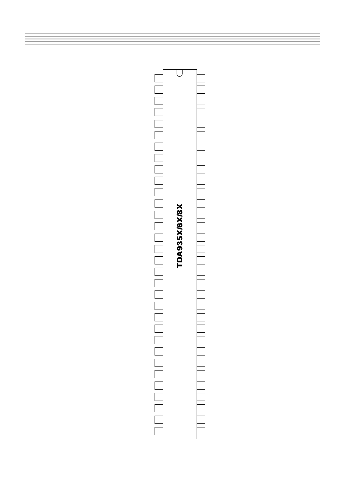
P1.3/T1
P1.6/SCL
P1.7/SDA
P2.0/TPMW
P3.0/ADC0
P3.1/ADC1
P3.2/ADC2
P3.3/ADC3
VSSC/P
P0.5
P0.6
VSSA
SECPLL
VP2
DECDIG
PH2LF
PH1LF
GND3
DECBG
AVL/EWD
VERB
VERA
IFIN1
IFIN2
IREF
VSC
TUNERAGC
AUDEEM/SIFIN1
DECSDEM/SIFIN2
GND2
SNDPLL/SIFAGC
AVL/REFO/AMOUT
P1.2/INT0
P1.1/T0
P1.0/INT1
VDDP
RESET
XTALOUT
XTALIN
OSCGND
VDDC
VPE
VDDA
BO
GO
RO
BLKIN
BCLIN
B2/UIN
G2/YIN
R2/VIN
INSSW2
AUDOUT/AMOUT
CHROMA
CVBS/Y
GND1
CVBSINT
VP1
IFVO/SVO
PLLIF
EHTO
AUDEXT/QSSO/AMOUT
FBISO
HOUT
1
2
3
4
5
6
7
8
9
10
11
12
13
14
15
16
17
18
19
20
21
22
23
24
25
26
27
28
29
30
31
32
64
63
62
61
60
59
58
57
56
55
54
53
52
51
50
49
48
47
46
45
44
43
42
41
40
39
38
37
36
35
.34
33
MXXxxx
TDA935X/6X/8X

-19-
Service Manual CP-785A
4-2 MSP34xxx Multistandard Sound Processor
The MSP34xxx is designed as a single-chip Multistandard Sound Processor for applications in
analogue and digital TV sets, video recorders, and PC cards.
MSP 3415D features
- sound IF input
- No external filters required
- Stereo baseband input via integrated AD converters
- Two pairs of DA converters
- Two carrier FM or NICAM processing
- AVC : Automatic Volume Correction
- Bass, treble, volume processing
- Full SCART in/out matrix without restrictions
- Improved FM-identification
- Demodulator short programming
- Autodetection for terrestrial TV - sound standards
- Precise bit-error rate indication
- Automatic switching from NICAM to FM/AM or vice versa
- Improved NICAM synchronisation algorithm
- Improved carrier mute algorithm
- Improved AM-demodulation
- Reduction of necessary controlling
- Less external components
Basic Features of the MSP 3415D
Demodulator and NICAM Decoder Section
The MSP 3415D is designed to simultaneously perform digital demodulation and decoding of NICAMcoded TV stereo sound, as well as demodulation of FM or AM mono TV sound. Alternatively, two
carrier FM systems according to the German terrestrial specs can be processed with the MSP 3415D.
The MSP 3415D facilitates profitable multistandard capability, offering the following advantages:
- Automatic Gain Control (AGC) for analogue input: input range: 0.10 - 3 Vpp
- integrated A/D converter for sound-IF input
- all demodulation and filtering is performed on chip and is individually programmable
- easy realisation of all digital NICAM standards (B/G, I, L and D/K)
- FM-demodulation of all terrestrial standards (include identification decoding)
- no external filter hardware is required
- only one crystal clock (18.432 MHz) is necessary
- high deviation FM-mono mode (max. deviation: approx. ±360 kHz)
CP-785A = DTE-25G5THS(FS-59T90)
MSP34xxx MSP3410D, 3415D, 3410G, 3415G Stereo(Nicam& 2-Carrier) DTE-29G5TH(FS-68T90)
CP-785AF=DTE-21U6TH(PF-51T31)
MSP3465G - Mono(Only AV Stereo) CP-785A=DTE-25G4ZH(FS-59V81)
DTE-29G4ZH(FS-68V81)

-20-
Service Manual CP-785A
DSP-Section (Audio Baseband Processing)
- flexible selection of audio sources to be processed
- performance of terrestrial de-emphasise systems (FM, NICAM)
- digitally performed FM-identification decoding and de-matrixing
- digital baseband processing: volume, bass, treble
- simple controlling of volume, bass, treble
Analogue Section
- two selectable analogue pairs of audio baseband input (= two SCART inputs) input level: <2 V RMS,
input impedance: >25 kΩ
- one selectable analogue mono input (i.e. AM sound): Not used in this chassis
- two high-quality A/D converters, S/N-Ratio: >85 dB
- 20 Hz to 20 kHz bandwidth for SCART-to-SCART copy facilities
- loudspeaker: one pair of four-fold oversampled D/A converters
output level per channel: max. 1.4 VRMS output resistance: max. 5 kΩ
S/N-ratio: >85 dB at maximum volume max. noise voltage in mute mode: < 10 V (BW: 20 Hz... 16 kHz)
- one pair of four-fold oversampled D/A converters supplying a pair of SCART-outputs.
output level per channel: max. 2 V RMS, output resistance: max. 0.5 kΩ
S/N-Ratio: >85 dB (20 Hz... 16 kHz)
Application Fields of the MSP 3415D
In the following sections, a brief overview about the two main TV sound standards, NICAM 728 and
German FM Stereo, demonstrates the complex requirements of a multistandard audio IC.
NICAM plus FM/AM-Mono
According to the British, Scandinavian, Spanish, and French TV-standards, high-quality stereo sound is
transmitted digitally. The systems allow two high-quality digital sound channels to be added to the
already existing FM/AM-channel. The sound coding follows the format of the so-called Near
Instantaneous Companding System (NICAM 728). Transmission is performed using Differential
Quadrature Phase Shift Keying (DQPSK. Table below offers an overview of the modulation parameters.
In the case of NICAM/FM (AM) mode, there are three different audio channels available: NICAM A,
NICAM B, and FM/AM-mono. NICAM A and B may belong either to a stereo or to a dual language
transmission. Information about operation mode and about the quality of the NICAM signal can be read
by the controlling software via the control bus. In the case of low quality (high bit error rate), the
controlling software may decide to switch to the analogue FM/AM-mono sound. Alternatively, an
automatic NICAM-FM/AM switching may be applied.
German 2-Carrier System (DUAL FM System)
Since September 1981, stereo and dual sound programs have been transmitted in Germany using the 2carrier system. Sound transmission consists of the already existing first sound carrier and a second sound
carrier additionally containing an identification signal. More details of this standard are given in Tables
below. For D/K very similar system is used.
-21-
Service Manual CP-785A
XTAL_IN
Audio PLL
D/A
D/A
FM1/AM
Demodulator
& NICAM
Decoder
Sound IF
FM2
NICAM A
NICAM B
IDENT
ANA_IN1+
Mono
MONO_IN
SC1_IN_L
SCART1
SC1_IN_R
SC2_IN_L
SCART2
SC2_IN_R
LOUD-
SPEAKER L
LOUDSPEAKER R
D/A
SCART1_L
SCART1_R
SCARTL
SCARTR
SCARTR Switching Facilities
D/A
A/D
A/D
DSP
SCART
SC1_OUT_R
SC1_OUT_L
Loudspeaker
DACM_L
DACM_R
XTAL_OUT
TV standards
TVsystem Position of sound carrier(MHz) Sound modulation Color system Remark
B/G 5.5 / 5.7421875 FM Stereo PAL Applied
B/G 5.5 / 5.85 FM-Mono / NICAM PAL Applied
L 6.5 / 5.85 AM - Mono / NICAM SECAM-L N.A
I 6.0 / 6.552 FM-Mono / NICAM PAL N.A
D/K 6.5 / 6.2578125 D/K1 FM Stereo SECAM-East
6.5 / 6.7421875 D/K2 N.A
6.5 / 5.85 D/K-NICAM FM-Mono / NICAM
Architecture of MSP3415D
Pin connections and short description
Pin No. Pin Name Type Short description
1 TP Out Test pin
2 NC Not Connected
3 NC Not Connected
4 TP Out Test pin
5 TP Out Test pin
6 ADR_SEL In I2C bus Address select
7 STANDBYQ In Standby ( Low-active)
8 NC Not Connected
9 I2C_CL In / Out I2C Clock
10 I2C_DA In / Out I2C data
11 TP In / Out Test pin
12 TP In / Out Test pin
13 TP Out Test pin
14 NC Not Connected
15 TP Out Test pin
-22-
Service Manual CP-785A
Pin No. Pin Name Type Short description
16 TP Out Test pin
17 TP Out Test pin
18 DVSUP Digital power supply +5V
19 DVSS Digital Ground
20 NC Not Connected
21 NC Not Connected
22 NC Not Connected
23 NC Not Connected
24 RESETQ In Power-On-reset
25 NC Not Connected
26 NC Not Connected
27 VREF2 Reference ground 2 high voltage part
28 DACM_R Out Loudspeaker out Right
29 DACM_L Out Loudspeaker out Left
30 NC Not Connected
31 TP Out Test pin
32 NC Not Connected
33 NC Not Connected
34 NC Not Connected
35 VREF1 Reference ground 1 high voltage part
36 SC1_OUT_R Out Scart output 1, right
37 SC1_OUT_L Out Scart output 1, left
38 NC Not Connected
39 AHVSUP Analog power supply 8.0V
40 CAPL_M Volume capacitor MAIN
41 AHVSS Analog ground
42 AGNDC Analog reference voltage high voltage part
43 NC Not Connected
44 NC Not Connected
45 NC Not Connected
46 NC Not Connected
47 NC Not Connected
48 ASG2 Analog Shield Ground 2
49 SC2_IN_L In Scart input 2 in, left
50 SC2_IN_R In Scart input 2 in, right
51 ASG1 Analog Shield Ground 1
52 SC1_IN_L In Scart input 1 in, left
53 SC1_IN_R In Scart input 1 in, right
54 VREFTOP Reference voltage IF A/D converter
55 MONO_IN In Mono input
56 AVSS Analog ground
57 AVSUP Analog power supply
58 ANA_IN1+ In IF input 1
59 ANA_IN1- In IF common
60 NC Not Connected
61 TESTEN In Test pin
62 XTAL_IN In Crystal oscillator
63 XTAL_OUT Out Crystal oscillator
64 NC Test pin
-23-
Service Manual CP-785A
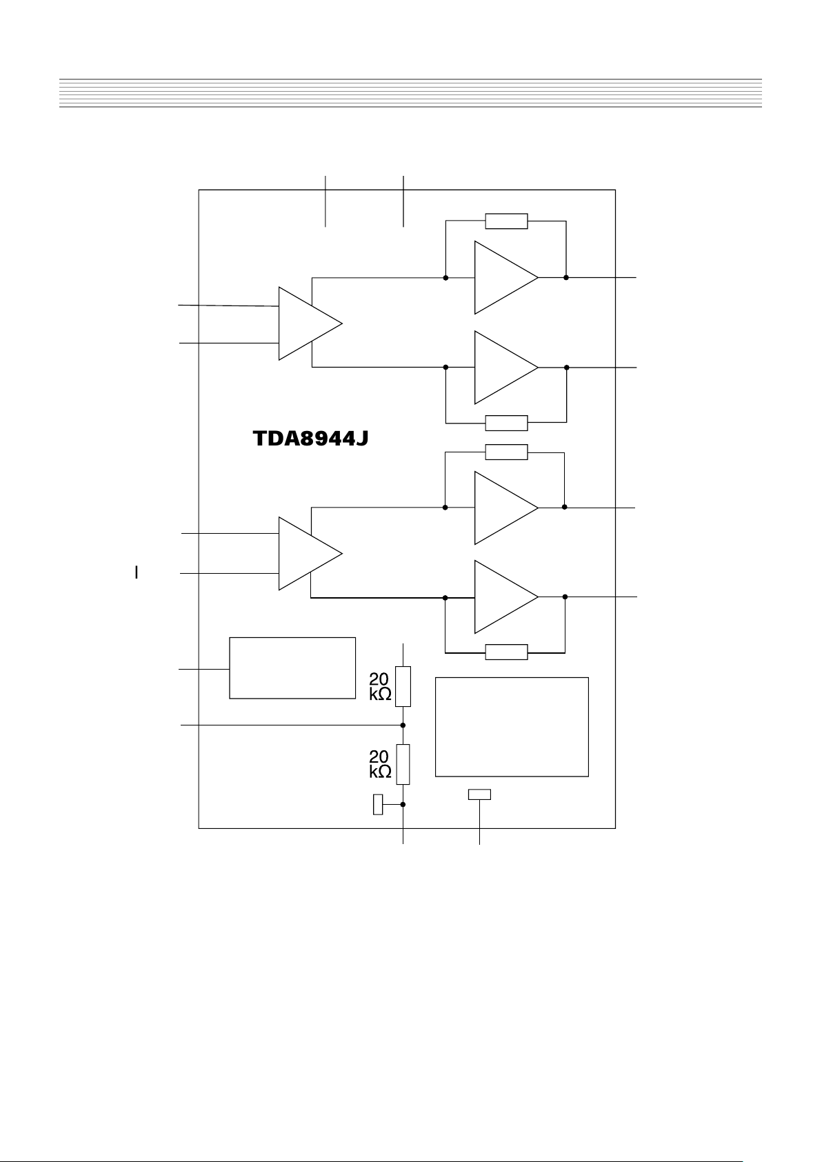
4-3 TDA894xJ family Stereo Audio Amplifier
The TDA8946J is a dua-channel audio power amplifier with an output power of 2 x 7W at an 8 ohm load
and a 12 V supply. The circuit contains two Bridges Tied Load (BTL) amplifiers with an all-NPN output
stage and standby/mute logic. The TDA8946J comes in a 17-pin DIL power package.
Features
Few external components
Fixed gain
Standby and mute mode
No on/off switching plops
low standby current
High supply voltage ripple rejection
Outputs short-circuit protected to ground, supply and across the load
Thermally protected
Pin description
Pin Symbol Description
1 OUT- negative loudspeaker terminal 1
2 GND1 ground channel 1
3 Vcc1 supply voltage channel 1
4 OUT1+ positive loudspeaker terminal 1
5 n.c. not connected
6 IN1+ positive input1
7 n.c. not connected
8 IN1- negative input1
9 IN2- negative input2
10 MODE mode selection input
11 SVR half supply voltage decoupling
(ripple rejection)
12 IN2+ positive input2
1
2
3
4
5
6
7
8
9
10
11
12
13
14
15
16
17
MBK936
OUT1-
GND1
Vcc1
OUT1+
n.c.
IN1+
n.c.
IN1-
IN2-
MODE
SVR
IN2+
n.c
OUT2+
GND2
Vcc2
OUT2-
TDA8944J
-24-
Service Manual CP-785A
V
CC1
V
CC
10
11
12
9
IN2-
TDA8944J
IN2+
MODE
SVR
STANDBY/
MUTE LOGIC
3 16
IN1-
IN1+
8
6
1
4
17
14
2 15
MBK933
OUT1-
OUT1+
OUT2-
OUT2+
GND2
GND1
SHORT CIRCUIT
AND
TEMPERATURE
PROTECTION
V
CC2
4-4 TDA835xJ Vertical Amplifier
The TDA835xJ are power circuit for use in 90° and 110° colour deflection systems for field frequencies
of 25 to 200Hz and 16/9 picture tubes. The circuit provides a DC driven vertical deflection output circuit,
operating as a highly efficient class G system. Due to the full bridge output circuit the deflection coils can
be DC coupled.
The IC is constructed in a Low Voltage DMOS process that combines Bipolar, CMOS and DMOS
devices. MOS transistors are used in the output stage because of the absence of second breakdown.
-25-
Service Manual CP-785A
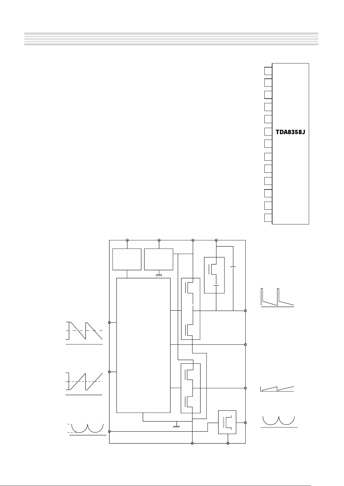
4-4-1 TDA8358J
An East-West output stage is provided that is able to sink current
from the diode modulator circuit.
Features :
Few external components
Highly efficient fully DC-coupled vertical output bridge circuit
Short rise and fall time of the vertical flyback switch
Guard circuit
Temperature (thermal) protection
High EMC because of common mode inputs
East-West output stage
V
i(pos)
V
i(neg)
V
p
V
oB
V
iew
GND
v
GND
EW
V
oEW
V
flb
V
oA
V
o(guard)
V
M
I
comp
1
2
3
4
5
6
7
8
9
10
11
12
13
TDA8358J
I
comp
V
0(guard)
V
p
93
M5
D3
D2
10
M2
M4
M4
M1
5
2
+V
i(diff)
V
i(sb)
-V
i(diff)
+V
i(diff)
V
i(sb)
-V
i(diff)
I
iEW(top)
I
iEW(bot)
V
i(neg)
1
M4
input/
feedback
V
i(neg)
V
i(pos)
M3
M6
8
4
7
6
12
D1
1113
comp
guard
V
flb
V
oA
V
M
V
oB
V
oEW
GND
EW
GND
V
-26-
Service Manual CP-785A
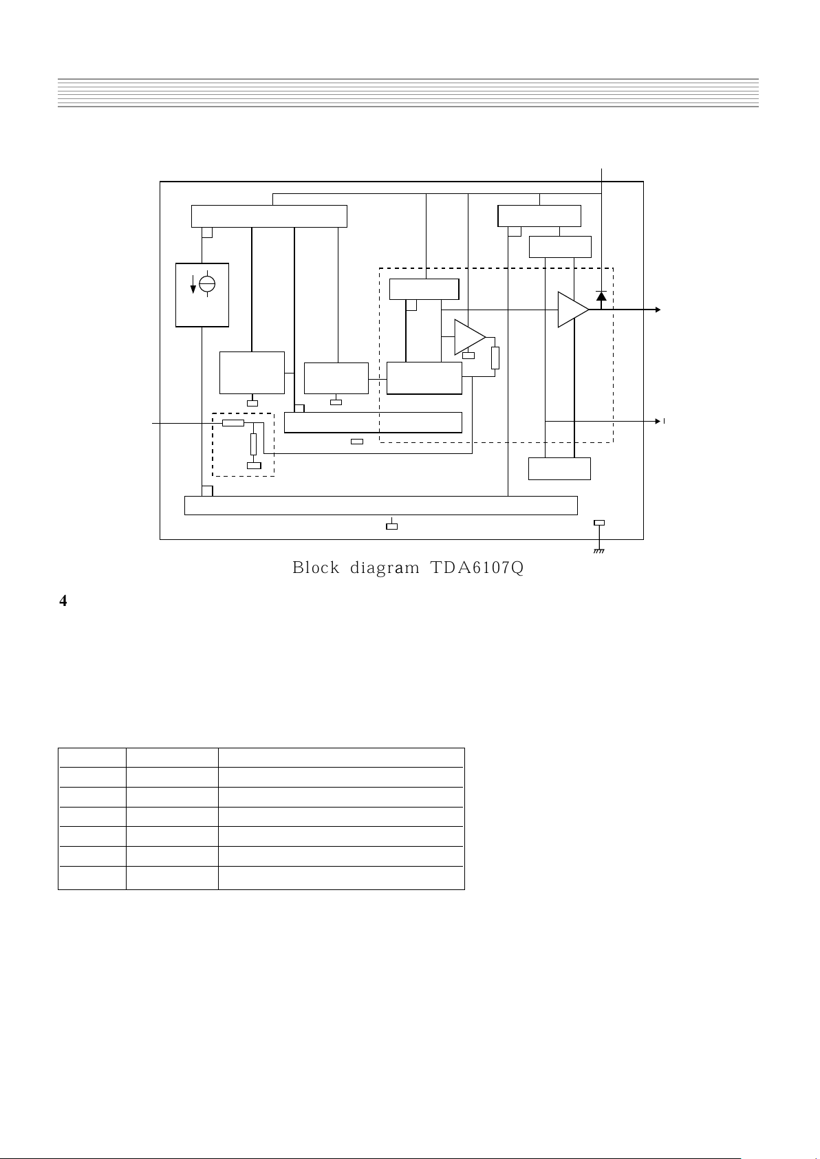
4-5 TDA6107Q
The TDA6107Q includes three video output amplifiers in one plastic DIL-Bent-SIL 9-pin medium power
package, using high voltage DMOS technology, and is intended to drive the three cathodes of a colour
CRT directly. To obtain maximum performance, the amplifier should be used with black-current control.
Features
Typical bandwidth of 5.5 MHz for an output signal of 60 Vpp
High slew rate of 900V/s
No external components required
Very simple application
Single supply voltage of 200V
Internal reference voltage of 2.5 V
Fixed gain of 50.
Black-current stabilisation (BCS) circuit
Thermal protection
Pin description
Pin Symbol Description
1 Vi(1) inverting input 1
2 Vi(2) inverting input 2
3 Vi(3) inverting input 3
4 GND ground (fin)
5 Iom black current measurement output
6 VDD supply voltage
7 VOC(3) cathode output 3
8 VOC(2) cathode output 2
9 VOC(1)
cathode output 1
Vi(1)
Vi(2)
Vi(3)
GND
Iom
VDD
Voc(3)
Voc(2)
Voc(1)
1
2
3
4
5
6
7
8
9
TDA6107Q
MGK277
-27-
Service Manual CP-785A
V
i(1),
V
i(2),
V
i(3)
1,2,3
R
i
R
a
3x
THERMAL
PROTECTION
CIRCUIT
VIP
REFERENCE
DIFFERENTIAL
STAGE
R
f
1x
3x3x
MIRROR 4
CASCODE 1
MIRROR 5
9,8,7
V
oc(3),
Voc(2),
V
oc(1)
MIRROR 3
MIRROR 2
MIRROR 1
CASCODE 2
4
MGK278
o(m)
V
DD
6
1x
TDA6107Q
CURRENT
SOURCE
BBlloocckk ddiiaaggrraamm TTDDAA66110077Q
Q
4-6 24C08 8 Kbit EEPROM
features :
8 Kbit serial I2C bus EEPROM
Single supply voltage : 4.5 V to 5.5 V
1 Million Erase/Write cycles (minimum)
40 year data retention (minimum)
Pin description
Pin No. Name Description
1,2,3 E0, E1, E2 Device address
5 SDA Serial Data/Address Input/Output
6 SCL Serial clock
7 WC Write contro
8 Vcc Supply voltage
4 Vss Ground
The memory device is compatible with the I2C memory standard. This is a two wire serial interface that
uses a bi-directionnal data bus and serial clock. The memory carries a built-in- 4-bit unique device type
identifier code (1010) in accordance with the I2C bus definition.
Serial Clock (SCL)
The SCL input is used to strobe all data in and out of the memory.
Serial Data (SDA)
The SDA pin is bi-directionnal, and is used to transfer data in or out of the memory

-28-
Service Manual CP-785A
4
Vin
3
Drain
1
OCP/FB
2
Source
5
GND
Rg2
Rg1
DR
V
DRV. REC=8.6V
Latch
O.V.P.
Start
Rcg.
T.S.D.
OSC
OCP/FB comp.
+
+
V(h2=1.3~1.6V
1.35mA
1NH comp.
T OFF=50 S typ.
STR-F6600 block diagram
4700pF
Iconst-trm.
Tth(min)=1 S
Vth1=0.73ᇹ0.05V
4-7 STR - F665X
4-7-1 General description
The STR-F6654 is an hybrid IC with a build-in MOSFET and control IC, designed for flyback converter
type switch mode power supply applications.
4-7-2 Features
Small SIP fully isolated molded 5 pins package
Many protection functions :
* Pulse-by-pulse overcurrent protection (OCP)
* Overvoltage protection with latch mode (OVP)
* Thermal protection with latch mode (TSD)
4-7-3 Block diagram

-29-
Service Manual CP-785A
4-7-4 Pins description
pin name symbol description
1 Overcurrent / feedback O.C.P./ F.B. Input of overcurrent detection signal and
feedback signal
2 Source S MOSFET source
3 Drain D MOSFET drain
4 Supply V
IN
Input of power supply for control circuit
5 Ground GND Ground
4-7-5 Control part electrical characteristics
IC pins symbol rating unit
description
number min. typ. max.
Operation start voltage 4-5 VIN(on) 14.4 16 17.6 V
Operation stop voltage 4-5 VIN(off) 9 10 11 V
Circuit current in operation 4-5 IIN(on) - - 30 mA
Circuit current in non-operation 4-5 IIN(off) - - 100 A
Maximum OFF time - T
OFF
(max) 45 - 55 sec
Minimum time for input of quaxi 1-5 T
TH
(2) - - 1.0 sec
resonant signals
Minimum off time - T
OFF
(min) - - 1.5 sec
O.C.P./F.B. terminal threshold 1-5 V
TH
(1) 0.68 0.73 0.78 V
voltage 1
O.C.P./F.B. terminal threshold 1-5 V
TH
(2) 1.3 1.45 1.6 V
voltage 2
O.C.P./F.B. terminal extraction 1-2 I
OCP/FB
1.2 1.35 1.5 mA
current
O.V.P. operation voltage 4-5 VIN(OVP) 20.5 22.5 24.5 V
Latch circuit sustaining voltage 4-5 IIN(H) - - 400 A
Latch circuit release voltage 4-5 VIN(La.off) 6.6 - 8.4 V
Thermal shutdown operating - T
J
(TSD) 140 - -
0
C
temperature
IC pins symbol rating unit
description
number min. typ. max.
Drain-to-source breakdown voltage 3-2 V
DSS
650 - - V
Drain leakage current 3-2 I
DSS
- - 300
A
On-resistance 3-2 RDS(on) - - 1.15
Switching time 3-2 tf - - 250 nsec
Thermal resistance -
CH -F
- - 0.95 oC/W
4-7-6 MOSFET electrical characteristics

-30-
Service Manual CP-785A
5 - Circuit description
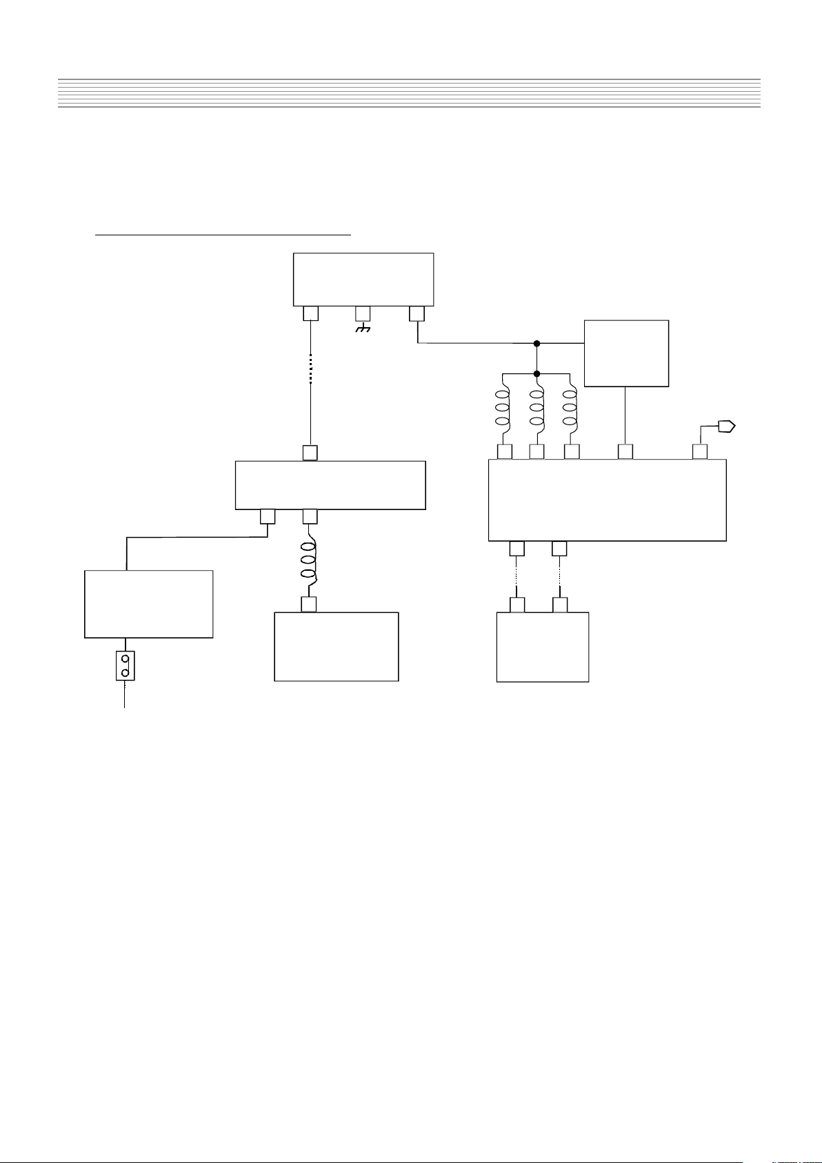
5-1 Block diagram
To speaker/
nead phones
II C BUS
I902
EEPROM(8K)
Audio
Amplifier
Base band signal
Sound processor I601
#28
#29
#49
#50
#52
#53
#36
#37
#58
SIF (5.5MHz for system B/G)
Audio out
scart 1
Audio in
scart 1
Audio in
scart 2
Trap 5.5MHz
video in
#51 #46 #40 #38 #35 #42
#52 #47
#53
#2 #3
#4-I501
#24
#23
#29
#28
Micro controller
Video IF
IF
IF = 38.9 MHz (All standard except L')
= 33.9 MHz (L')
Audio IF
SF1 SF2
Video
processor
I501
#48
video
out
QSS
out
ext, video in
Video in
SCART 1
Switching
circuit
SCART 2
Switch control
from #8-i501
and #8 SCART 1
RGB out
To CRT board
ext RGB in
chroma in
I602

-31-
Service Manual CP-785A
FUNCTIONAL DESCRIPTION OF VIDEO PROCESSOR Vision IF amplifier
The vision IF amplifier can demodulate signals with positive and negative modulation. The PLL
demodulator is completely alignment-free.
The VCO of the PLL circuit is internal and the frequency is fixed to the required value by using the clock
frequency of the -Controller/Teletext decoder as a reference. The setting of the various frequencies is
made by the controlling software in subaddress 27H (38.9 Mhz for all system). Because of the internal
VCO the IF circuit has a high immunity to EMC interferences.
QSS Sound circuit
The sound IF amplifier is similar to the vision IF amplifier
and has an external AGC decoupling capacitor.
The single reference QSS mixer is realised by a multiplier. In this multiplier the SIF signal is converted
to the intercarrier frequency by mixing it with the regenerated picture carrier from the VCO. The mixer
output signal is supplied to the output via a high-pass filter for attenuation of the residual video signals.
With this system a high performance hi-fi stereo sound processing can be achieved.
Video switches
The video switch has one input for an external CVBS or Y/C signal. The selected CVBS signal can be
supplied to pin 38, the IF video output. The selection between both signals is realised by the controlling
software in subaddress 22H.
The video ident circuit is connected to the selected signal. This ident circuit is independent of the
synchronisation.
Synchronisation circuit
The IC contains separator circuits for the horizontal and vertical sync pulses and a data-slicing circuit
which extracts the digital teletext data from the analogue signal.
The horizontal drive signal is obtained from an internal VCO which is running at a frequency of 25 MHz.
This oscillator is stabilised to this frequency by using a 12 MHz signal coming from the reference
oscillator of the -Controller/Teletext decoder.
The horizontal drive is switched on and off via the soft start/stop procedure. This function is realised by
means of variation of the TON of the horizontal drive pulses.
The vertical synchronisation is realised by means of a divider circuit. The vertical ramp generator needs
an external resistor and capacitor. For the vertical drive a differential output current is available. The
outputs are DC coupled to the vertical output stage.

-32-
Service Manual CP-785A
In the TDA936x series, the following geometry parameters can be adjusted for all picture tubes :
Horizontal shift
Vertical amplitude
Vertical slope
S-correction
Vertical shift
The types which are intended to be used in combination with 110° picture tubes have an East-West
control circuit. The additional controls for these types are:
EW width
EW parabola width
EW upper and lower corner parabola correction
EW trapezium correction
Vertical zoom, horizontal parallelogram and bow correction.
Chroma and luminance processing
The chroma band-pass and trap circuits (including the SECAM cloche filter) are realised by means of
gyrators and are tuned to the right frequency by comparing the tuning frequency with the reference
frequency of the colour decoder. The luminance delay line and the delay cells for the peaking circuit are
also realised with gyrators. The circuit contains a black stretcher function which corrects the black level
for incoming signals which have a difference between the black level and the blanking level.
Colour decoder
The ICs can decode PAL, NTSC and SECAM signals. The PAL/NTSC decoder does not need external
reference crystals but has an internal clock generator which is stabilised to the required frequency by
using the 12 MHz clock signal from the reference oscillator of the -Controller/Teletext decoder.
The Automatic Colour Limiting (ACL) circuit (switchable via the ACL bit in subaddress 2OH) prevents
that oversaturation occurs when signals with a high chroma-to-burst ratio are received. The ACL circuit
is designed such that it only reduces the chroma signal and not the burst signal. This has the advantage
that the colour sensitivity is not affected by this function.
SOFTWARE CONTROL
The CPU communicates with the peripheral fonctions using Special function Registers (SFRS) which are
addressed as RAM locations. The registers for the Teletext decoder appear as normal SFRs in the Controller memory map and are written to these functions by using a serial bus. This bus is controlled by
dedicated hardware which uses a simple handshake system for software synchronisation.
For compatibility reasons and possible re-use of software blocks, the TV processor is controlled by I2C
bus. The TV processor control registers cannot be read. Only the status registers can be read ( Read
address 8A ).
The SECAM decoder contains an auto-calibrating PLL demodulator which has two references, via the
divided 12 MHz reference frequency (obtained from the
-Controller) which is used to tune the PLL to

-33-
Service Manual CP-785A
the desired free-running frequency and the bandgap reference to obtain the correct absolute value of the
output signal. The VCO of the PLL is calibrated during each vertical blanking period, when the IC is in
search or SECAM mode.
The base-band delay line (TDA 4665 function) is integrated. This delay line is also active during NTSC
to obtain a good suppression of cross colour effects. The demodulated colour difference signals are
internally supplied to the delay line.
RGB output circuit and black-current stabilisation
In the RGB control circuit the signal is controlled on contrast, brightness and saturation. The ICs have a
linear input for external RGB signals. The signals for OSD and text are internally supplied to the control
circuit. The output signal has an amplitude of about 2 Volts black-to-white at nominal input signals and
nominal settings of the various controls.
To obtain an accurate biasing of the picture tube the 'Continuous Cathode Calibration’ system has been
included in these ICs. A black level off set can be made with respect to the level which is generated by
the black current stabilisation system. In this way different colour temperatures can be obtained for the
bright and the dark part of the picture.
The black current stabilisation system checks the output level of the 3 channels and indicates whether the
black level of the highest output is in a certain window or below or above this window. This indication is
read from the status byte 01 and is used for automatic adjustment of the Vg2 voltage during the
production of the TV receiver.
During switch-off of the TV receiver a fixed beam current is generated by the black current control
circuit. This current ensures that the picture tube capacitance is discharged. During the switch-off
period the vertical deflection is placed in an overscan position so that the discharge is not visible on the
screen.

-34-
Service Manual CP-785A
5-2 IF
The TDA936x has an alignment free IF PLL demodulator. The fully integrated oscillator is automatically
calibrated, using the 12 Mhz crystal as a frequency reference. The IF frequency is simply set in TVProcessor by I2C bus.
The AFC information is available via I2C bus from the TV-Processor status bytes. The controlling
software uses this information for tuner frequency tracking ( automatic following ). The AFC windows is
typically 125Khz wide. The minimum frequency step of the tuner is 62.5 Khz.
This AFC function is disabled when a program is tuned using the direct frequency entry or after fine
tuning adjustment. Therefore it is recommended to tune channel with the TV search function ( manual or
Auto setup) or using the direct channel entry to enable the Automatic Frequency Control.
SAW filters
Ref. Standard Features
K3953M B/G - IF filter for video application
- TV IF filter with Nyquist slopes at 38.9 MHz
- Constant group delay
K9650M B/G - IF filter for audio application
- TV IF audio filter with two channels
- Channel ( B/G) with one pass band for sound
carriers 33.40 MHz
The SAW filter ( SF1 ) has a double Nyquist slope at 38.9 MHz needed for this multistandard
application. The disadvantage of this choice is that a 5.5 MHz trap filter ( Z501 ) is needed to suppress
the residual sound carrier in the video for B/G signals.

-35-
Service Manual CP-785A
5-3 Source switching
The TDA936x has only one external video input, the external video switching circuit made with Q504,
Q505 and Q508 allows 2 external video signal inputs. The switching command can be the -Controller pin
8 when the software takes control of the video source.
The -Controller pin 8 is automatically configured by the controlling software (See table below).
TV mode -Controller pin 8 Status Level
RF auto Input - High Impedance < 1V
RF Forced Input - High Impedance not defined
AV 1 Input - High Impedance > 2.0 V
AV 1 Output - Push Pull Max. 3.3V
AV 2 Output - Push Pull < 0.2 V
SVHS Output - Push Pull < 0.2 V
The controlling software via I2C bus selects the signal source :
- Video signal from tuner ( Pin 40 ).
- External video ( SCART 1 or 2 ) depending on Q508 base level.
- External SVHS from SCART 2.
The sound source switching is done in the MSP3415D ( I601 ), by the -Controller via I2C bus.
Fast R, G, B insertion : The external R, G, B insertion needs a fast switching and cannot be controlled by
the software ( instruction cycle of 1 sec ). The fast switching pin 16 of SCART 1 is directly connected to
the TV processor pin 45 ( Fast blanking input ). The display is synchronised with the selected video
source, i.e. to get stable R, G, B inserted signal they must be synchronised with the selected video source.
The controlling software only enable or disable ( AV2, SVHS, or Forced RF source selected ) fast
blanking.
5-4
-Controller I/O pin configuration and function
The I/O pins of the -Controller can be configured in many way. All port functions can be individually
programmed by use of the SFR registers.
Each I/O port pin can be individually programmed in these configurations :
Open drain
In this mode, the port can function as in and output. It requires an external pull-up resistor. The maximum
allowable supply voltage for this pull up resistor is +5V.
So in this mode it is possible to interface a 5 Volt environment like I2C while the -Controller has a 3.3
Volt supply.
Push-Pull
The push pull mode can be used for output only. Both sinking and sourcing is active, which leads to sleep
slopes. The levels are 0 and Vddp, the supply voltage 3.3Volts.

-36-
Service Manual CP-785A
High impedance
This mode can be used for input only operation of the port.
Special port for LED
Pin 10 and 11 have the same functionality as the general I/O pins but in addition, their current source and
sink capacity is 8 mA instead of 4 mA. These pins are used for driving LED’ s via a series current
limiting resistor.
-Controller I/O pin configuration and function table
pin name configuration description
Stand by TV ON
1 n.u. High impedance High impedance not used
2 SCL Open Drain Open Drain Serial clock line
3 SDA Open Drain Open Drain Serial data line
4
5 OCP High impedance High impedance Over Current Protection
( Switch the set OFF if
the voltage on this pin is
<2.33V )
6 - High impedance High impedance For factory use only
7 Key in High impedance High impedance Local keyboard input
8 S/SW High impedance See table above external video switch
10 Red LED High impedance Open Drain
11 Green LED Open Drain High impedance
62 Audio mute Push Pull Push Pull High in stand by mode
5-5 Sound processing
Analogue sound IF - input section
The input pins ANA_IN1+ and ANA_IN- offer the possibility to connect sound IF sources to the MSP
3415D. The analogue-to-digital conversion of the preselected sound IF signal is done by an A/D
converter, whose output is used to control an analogue automatic gain circuit (AGC), providing an
optimal level for a wide range of input levels.
Quadrature Mixers
The digital input coming from the integrated A/D converter may contain audio information at a frequency
range of theoretically 0 to 9 MHz corresponding to the selected standards. By means of two
programmable quadrature mixers, two different audio sources ; for example, NICAM and FM-mono,
may be shifted into baseband position.
Phase and AM discrimination
The filtered sound IF signals are demodulated by means of the phase and amplitude discriminator block.
On the output, the phase and amplitude is available for further processing. AM signals are derived from
the amplitude information, whereas the phase information serves for FM and NICAM demodulation.

-37-
Service Manual CP-785A
In case of NICAM - mode, the phase samples are decoded according the DQPSK - coding scheme. The
output of this block contains the original NICAM bitstream.
DSP section
All audio baseband functions are performed by digital signal processing (DSP). The DSP section controls
the source and output selection, and the signals processing.
Sound Mode switching
In case of NICAM transmission, the controlling software read the bit error rate and the operation mode
from the NICAM Decoder. When the set is in “Auto detection” mode ( default mode after ATSS ) the
controlling software set automatically the sound mode ( NICAM mono, NICAM Dual 1 or NICAM Dual
2 ) depending on the transmitted mode.
In case of 2 Carrier FM transmission, the controlling software read the transmission mode and the signal
quality level from the Stereo Detection Register. When the set is in “Auto detection” mode the
controlling software set automatically the sound mode ( mono, Stereo, Dual 1, Dual 2 ) depending on the
transmitted mode.
In “Auto detection” mode the controlling software evaluate the signal quality and automatically switch
to the analogy sound carrier 1, if the transmission quality is too poor. To avoid unwanted automatic
switching the threshold levels mono to stereo and stereo to mono is different. In “forced mono “ mode (
Red OSD in recall section ), the controlling software configure the MSP3415D to demodulate only the
analogue (FM or AM) sound carrier 1, no matter the signal quality.
The sound mode “ forced “ or “ Autodetect” is stored for each programme.
5-6 Sound amplification
The TDA8946J is a stereo BTL audio amplifier capable of delivering 2 x 7 W output power to an 8
load at THD = 10%, using a 12 V power supply and an external heatsink. The voltage gain is fixed at
32dB.
With the three-level MODE input the device can be switched from ‘ standby’ to ‘ mute’ and to ‘
operating’ mode.
The TDA 8946J outputs are protected by an internal thermal shutdown protection mechanism and shortcircuit protection.
Power amplifier
The power amplifier is a Bridge Tied Load (BTL) amplifier with an all-NPN output stage, capable of
delivering a peak output current of 1.5 A.
The BTL principle offers the following advantages :
- Lower peak value of the supply current.
- The ripple frequency on the supply voltage is twice the signal frequency.
- No DC-blocking capacitor
- Good low frequency performance
Mode selection
The TDA894xJ has several functional modes, which can be selected by applying the proper DC voltage
to pin MODE.

-38-
Service Manual CP-785A
Mute : In this mode the amplifier is DC biased but not operational (no audio output). This allows the
input coupling capacitors to be charged to avoid pop-noise. The devices is in mute mode when 2.5 V <
VMODE < (Vcc-1.5 V).
Operating : In this mode the amplifier is operating normally. The operating mode is activated at VMODE
< 0.5 V.
5-7 Vertical deflection
The vertical driver circuit is a bridge configuration. The deflection coil is connected between the output
amplifiers, which are driven in phase opposition. The differential input circuit is voltage driven. The
input circuit is especially intended for direct connection to driver circuits which deliver symmetrical
current signals, but is also suitable for asymmetrical currents. The output current of these devices is
converted to voltages at the input pins via resistors R350 and R351. The differential input voltage is
compared with the output current through the deflection coils measured as voltage across R302, which
provides internal feedback information. The voltage across R302 is proportional to the output current.
Flyback voltage
The flyback voltage is determined by an additional supply voltage Vflb. The principle of operation with
two supply voltages (class G) makes it possible to fix the supply voltage Vp optimum for the scan
voltage and the second supply voltage Vflb optimum for the flyback voltage. Using this method, very high
efficiency is achieved. The supply voltage Vflb is almost totally available as flyback voltage across the
coil, this being possible due to the absence of a coupling capacitor.
Protection
The output circuit has protection circuits for :
- Too high die temperature
- overvoltage of output stage A
Guard circuit
The guard signal is not used by the TDA936x to blank the screen in case of fault condition.
Damping resistor
For HF loop stability a damping resistor (R305) is connected across the deflection coil.
EAST-WEST Amplifier (TDA8358J only)
The East-West amplifier is current driven. It can only sink currents of the diode modulator circuit. A
feedback resistor R397 is connected between the input and output of this inverting amplifier in order to
convert the East-West correction input into an output voltage.

-39-
Service Manual CP-785A
5-8 Power supply (STR-F6654)
5-8 -1 STR-F6654 general description
The STR-F6654 is an hybrid IC with a build-in MOSFET and control IC, designed for flyback converter
type switch mode power supply applications.
5-8 -2 Power supply primary part operations
An oscillator generates pulses signals which turn on and off a MOSFET transistor.
* Start -up circuit: VIN
The start-up circuit is used to start and stop the operation of the control IC, by detecting a voltage
appearing at VIN pin (pin 4).
R8 19
D8 0 2
D8 0 1
D8 0 3
D8 0 4
C8 0 4
C8 0 3
R8 02
C8 0 6
C8 0 5
Ma in A C vo ltag e
2
D8 0 5
R8 05
L8 0 1
4
Gr o und
Dr a in Vi n
T80 1 S MPS T R A NS
3
I8 01 S TR-F 665 3
5
Power supply start-up circuit
7
6
4

-40-
Service Manual CP-785A
When the power switch is pushed on, VIN increases slowly. During this time, C806 is charged through
R802.
As soon as VIN reaches 16V, the STR-F6654 control circuit starts operating. Then, VIN is obtained by
smoothing the winding voltage which appears between pin6 and pin7 of the SMPS transformer.
As this winding voltage does not increase to the set voltage immediately after the control circuit starts
operating, VIN starts dropping. However, as this winding voltage reaches the set value before VIN voltage
drops to the shutdown voltage (at 11V), the control circuit continues operating (see below VIN voltage at
start-up). R805 resistor prevents that VIN pin voltage varies according to the secondary side output
current.
VIN must be set higher than the shutdown voltage (VIN (off) = 11Vmax) and lower than the O.V.P.
(overvoltage protection) operating voltage
(VOVP = 20.5Vmin)
Shutdown voltage 11V
16V ( T Y P.)
O.V.P. voltage 20.5V
Vi n
t
Waveform of Vin pin voltage at start-up
-41-
Service Manual CP-785A
* STR-F665X oscillating operation
TO P I N4 SM PS
2
3
1
5
G N D
R804
C850
OC P /FB
Fr o m P I N 6
SM PS
(FEEDBACK)
SO U RCE
R808
D R A IN
D R I V E
OS C
Rg2
Rg1
Co mp. 2
Co mp. 1
C1
R1
STR - F 6 6 5 0
1. 35m A
V th(1 )
V th(2 )
Oscillating operation
O N
O N O N
O F F
O F FO F F
M O S F E T s w i t c h i n g O N / O F F
V
D S
( M O S F E T d r a i n - s o u r c e v o l t a g e )
I
D
( M O S F E T d r a i n c u r r e n t )
P i n 1
( O C P / F B )
0 V
0 . 7 3 V
( S T R - F 6 6 5 3
i n t e rn a l c a pa c i t o r )
C 1
3 . 7 V
6 . 5 V
1
3
2
4
Waveforms during oscillating operation

-42-
Service Manual CP-785A
When the MOSFET is ON, the STR-F6650 internal capacitor C1 is charged at the constant voltage
6.5V.
At the same time, the voltage at pin 1 (OCP / FB) increases with the same waveform as the MOSFET
drain current.
When the pin 1 voltage reaches the threshold voltage VTH1 = 0.73V, the STR-F6650 internal
comparator 1 starts operating. The STR-F6650 internal oscillator is inverted and the MOSFET turns OFF.
When the MOSFET turns OFF, charging of STR-F6650 internal capacitor C1 is released and C1
starts discharging by the STR-F6654 internal resistance R1. So, C1 voltage starts falling in accordance
with the gradient regulated by the constant discharging time of C1 and R1. So, this means that the fixed
time determined by C1 and R1 is the OFF-time of the MOSFET.
When C1 voltage falls to around 3.7V, the STR-F6650 internal oscillator is reversed again and the
MOSFET turns ON. C1 is quickly charged to around 6.5V
The MOSFET continues to oscillate by repeating the above procedure.
* STR-F6650 protection circuits
overcurrent protection function (OCP)
Overcurrent protection is performed pulse by pulse detecting at STR-F6654 pin 1 (OCP) the peak of the
MOSFET drain current in every pulse.
latch circuit
This circuit sustains an output low from the STR-F6654 internal oscillator and stops operation of the
power supply when overvoltage protection (OVP) and thermal shutdown (TSD) circuit are under
operation
thermal shutdown circuit (TSD)
This circuit triggers the latch circuit when the frame temperature of STR-F6654 IC exceeds 140°C
overvoltage protection circuit (OVP)
This circuit triggers the latch circuit when the V
in voltage exceeds 22V (typ.)
-43-
Service Manual CP-785A
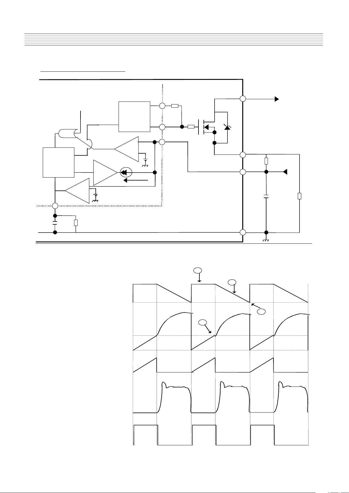
5-9 TV start-up, TV normal run and stand-by mode operations
5-9-1 TV start-up operations
* Schematic diagram for start-up operations
I8 2 3 RE G 3.3 V
IN
GND
OUT
1
2 3
RES E T
PULS E
CIR C U I T
IN
OUT
63
60
54
5661
L5 1 1
L5 1 0
L5 1 2
Vd dc
Vd d A
Re set N
Po w er
I5 01
MICROCONTROLLER P AR T
SCL
SD A
3
2
56
3
4
2
D
I80 1 M O SFET AND
CONTR OL IC
I7 02
EEPRO M
SW 8 01
POWER S W I T C H
MAIN AC V OL T A G E
D80 1 . . . D80 4
(GR A E T Z BR I D G E)
L8 0 1
T80 1 SM PS TR ANSF ORMER
12
8V
Vd dp
Start-up operations
* TV start-up and microcontroller initialization
- When SW801 power switch is pushed, main AC voltage is applied to T801 transformer (after
rectification by D801...D804 diodes). Then, T801 SMPS transformer starts operating and supplies DC
voltage to I823 (3.3V regulator).
- This regulator provides 3.3V DC voltage to I501 microcontroller power supply pins (pins 54, 56, 61)
and to the reset pulse circuit which provides reset pulse to I501 microcontroller reset pin (pin 60).
- Then, the microcontroller starts its initialization. Its power pin (pin 63) is set to high which allows
delivery of power supply voltages (123V, 8V, 5V...). At this step, all IC’ s start working but no picture
appears on screen: I501 IC doesn’ t provide horizontal drive voltage.
- Then, the microcontroller consults I702 EEPROM via I2C bus to know the last TV set mode (normal
run mode or stand-by mode ) before switching off.

-44-
Service Manual CP-785A
. If the TV set was on normal run mode before switching off, the microcontroller delivers horizontal drive
voltage at pin 33 and picture appears on screen.
. If the TV set was on stand-by mode before switching off, the microcontroller switches TV set to standby mode, decreasing power pin voltage (pin 63). This matter will be explained on paragraph 5-9-2-b.
* Reset pulse circuit
3.3V
3.0V
3.0V
1.2V
1.2V
0V
DC supply voltage
I823 pin 3
reset pulse
I501 pin 60
from I823
pin 3
R591
220
Ω
D591
DZ2.4
R593
10K
Ω
R592
10k
Ω
Q510
R594
10K Ω
Q511
C501
50V
10
µ
F
to I501
pin 60
+
0
V
Reset pulse circuit and corresponding waveforms

-45-
Service Manual CP-785A
* Reset pulse circuit operations description
- When DC supply voltage from I823 regulator starts rising (from 0V to 1.2V), no current flows through
D591 zener diode. So, Q510 is in off mode.
Also Vbe Q511 =Vcc/2 -Vcc = -Vcc/2 > -0.6V. So, Q511 is in off mode.
Then, no voltage reaches I501 pin 60.
- When this voltage reaches 1.2 V, Q510 stays in off mode
but Vbe Q511 = -0.6V. So, Q511 is switched on and starts driving DC supply voltage to I501 pin 60.
- When the DC supply voltage reaches (2.4V +0.6V ) =3.0V, Q510 starts conducting but as the Q511
base-emitter voltage is the same as the collector-emitter voltage of the saturated Q510, Q511 switches off
and no voltage reaches I501 pin 60.
- If the DC supply voltage decreases below 3 V, Q510 switches off immediately. Q511 starts conducting,
pulling I501 pin 60 high.
At the same time, it discharges the reset capacitor C501. Discharging this capacitor is necessary to
garantee a defined reset pulse duration.
5-9-2 TV normal run and stand-by mode operations
Depending on remote control commands, I501 microcontroller part pin 63 (power) is set to:
- high for normal run mode
- low for stand-by mode
a) TV on normal run mode
* I501 microcontroller part pin 63 (power) effect
I501 microcontroller part pin 63 (power) is connected to the following circuit:
I 8 1 0
C O N T R O L L E D
R E C T I F I E R
R 8 2 0
R 8 3 0
C 8 3 0
R 8 2 9
Q 8 0 8
6 V D C
1 1 V D C
R 8 7 0
D 8 1 1
Q 8 1 1
Q 8 0 9
Q 8 0 7
Q
8 1 0
L O W
L O W
L O W
L O W
H I G H
H I G H
C O N D U C T I N G
P O W E R
H I G H
N O T
C O N D U C T I N G
I501 microcontroller part pin 63 (POWER) effect

-46-
Service Manual CP-785A
On normal run mode, I501 microcontroller pin 63 (power) is set to high
So, I810 controlled rectifier is not conducting
- Q809 is conducting. So, Q808 is not conducting and Q807 is conducting
- So, Q807 collector is connected to the ground and I810 controlled rectifier gate pin is
set to low (no conducting)
So, current from 11V DC voltage (from T801 SMPS transformer pin 13) does not flow through
Q811 and Q810 transistors but flows through I806 IC error amplifier
- Q809 is conducting. So, Q810 is not conducting and no current flows from Q810
collector to the ground
Therefore, the power supply circuit diagram is the one shown on the next paragraph
* power supply circuit diagram during TV set normal run
I 8 2 0
5 V
R E G U L A T O R
I 8 2 3
3 . 3 V
R E G U L A T O R
1 4 . 5 V ( C P 7 8 5 )
1 2 . 5 V ( C P 3 8 5 )
5 V
3 . 3 V
3
3
1
1
1 1 V
8 V
6 V
1
3
1 4 3 V ( C P 7 8 5 )
1 2 3 V - 1 1 3 V ( C P 3 8 5 )
D 8 2 0
D 8 6 0
D 8 3 0
D 8 3 1
C 8 3 2
C 8 2 3
C 8 6 1
9
1 2
1 3
1 6
2
4
C 8 1 3
R 8 2 3
R 8 1 0
1 1 V
2
3
I 8 0 6
I C E R R O R A M P L I F I E R
1 4 . 5 V
1 2 . 5 V
8 . 5 V
8 V
1 1 . 5 V
1 1 V
1 4 3 V
1 2 3 V / 1 1 3 V
T 8 0 1 S M P S T R A N S F O R M E R
D 8 0 1 . . . D 8 0 4
( G R A E T Z B R I D G E )
D
I 8 0 1
M O S F E T A N D
C O N T R O L IC
S W 8 0 1
P O W E R
S W I T C H
M A I N A C V O L T A G E
L 8 0 1
Ι 82 2
8
V
R E G U L A T O R
1
3
Power supply operation during TV set normal run

-47-
Service Manual CP-785A
* power supply functioning during TV set normal run mode
- I801 transmits controlled pulses to T801 which generates DC voltages after rectifications by secondary
part diodes and electro capacitors (by example by D820 and C813 on 143V supply voltage line).
- 8V, 5V, 3.3V supply voltage lines have stabilized voltages obtained by I820, I822, I823 voltage
regulators.
- On 143V supply voltage line, R823 resistor has been chosen to reach exact DC voltage required on this
line.
- 143V supply voltage line includes an IC error amplifier (I806) which corrects unexpected DC voltage
variations on this line.
* power supply IC delivery during TV set normal run
power supply line IC power supply delivery Remarks
FBT supplies 45V to I301 vertical IC
FBT supplies 45V to T401 H- drive
143V FBT FBT supplies 14V to I301 vertical IC
FBT supplies 33V to the tuner
FBT supplies 185V to I901 video amplifier pin 6
12.5V I602 sound amplifier pins 3-16
11V T401 H- drive
8V I501 Main IC pins 14-39
I601 Sound Demod pins 38-39-40
6V I703 IR receiver pin 1
I601 Sound Demod pins 7-18-57
5V I702 EEPROM pin 8
tuner
3.3V Main IC com part pins 54-56-61
b) TV set on stand-by mode
* TV set circuit diagram on stand-by mode

-48-
Service Manual CP-785A
2
4
3
D RA IN
I801
MOF SET AND
CO NTR OL IC
1
MAI N AC V OLTA G E
I804
OPTO
COU PLER
I8 23 3. 3V
REG UL ATO R
I7 03 I R
RE CE IV ER
FR ON T
M A SK
B U T T O N S
I8 10
C O NTR OL LE D
RE CTI FI ER
SWI TC HI NG
CIR CU I T
T801 SM PS TRA NS
I501
MA I N
IC
OCP
FB
16
D821
I810
controlled rectifier
HI GH
C841
C840
R713
1
3
1
2
616456
54
7
63
CO N DUC T IN G
I R I N
µ
com
supply
voltage
K E Y IN
PO WER
R888
C888
Q809
Q810
Q811
D811
D825
R810
L801
D806
C808
SW801
POWER S WI TC H
C850
R806
8
4
3
1
2
R870
HI GH
LO W
LO W
CO N DUC T IN G
CO N DUC T IN G
AR OU ND
6Vdc
AR OU ND
3.3Vdc
Power supply operation in stand - by mode
D801...D804
GRAETZ BRIDGE

-49-
Service Manual CP-785A
I810
CONTROL L E D
REC T I F I E R
R8 20
R8 30
C8 30
R8 29
Q8 08
6V DC
Q8 09
Q
80 7
HIGH
HIGH
HIGH
LOW
POWER
I810 controlled rectifier switching circuit
* TV set stand-by mode operations
-On stand-by mode, I501 microcontroller pin 63 (power) is set to low.
- So, Q809 collector is set to high.
-Then, I810 controlled rectifier gate pin is set to high and I810 is conducting.
- So, current flows from pin 16 SMPS transformer to the ground via I804 optocoupler and Q810 and
Q811 transistors (which are conducting).
- In these conditions, I801 delivers pulses on light mode and T801 produces voltages with reduced
power.
- As I810 is conducting, current flows also from pin 16 SMPS transformer to I823 (3.3V regulator) for
I501 com, IR receiver and front mask buttons supply voltage (then, remote control or front mask
buttons can be activated to leave stand-by mode).
-50-
Service Manual CP-785A
LOC PART NAME PART Code PART Description Remark
ZZ100 TRANSMITTER REMOCON 48B4744N08 R-44N08 (AA) With Text (RD-D90)
48B4744N09 R-44N09 (AA) Without Text (RD-D85)
00010 BATTERY 4850Q00810 R6P/LN
00030 CABLE SCART 4859000160 S-RCA 3P/DIN 4P(1.2M) FS-xxT90 only
ZZ120 COVER BACK AS PTBCSHD393 DTE-29G5TH FS-68T90
PTBCSHD392 DTE-25G5THS FS-59T90
PTBCSHD635 DTE-29G4ZH FS-68V81
PTBCSHD634 DTE-25G4ZH FS-59V81
ZZ131 CRT GROUND NET 48519A4210 2901H-1015-2P 29 inch (2pin Type - old)
48519A6410 2901S-1015-1P 29 inch (1pin Type - New)
48519A4010 2501H-1015-2P 25 inch (2pin Type - old)
48519A6310 2501S-1015-1P 25 inch (1pin Type - New)
ZZ132 COIL DEGAUSSING 58G0000145 DC-29S2 29 inch
58G0000144 DC-25S2 25 inch
V901 CRT 4859633867 A68KTB359X010(B) M50 29 inch (6pin DY - old)
4859633769 A68KTB359X001(B) M50 29 inch (4pin DY- New)
4859629569 A59KPR84X02(D) M50 25 inch (6pin DY - old)
4859629069 A59KPR84X01(D) M50 25 inch (4pin DY- New)
ZZ200 MASK FRONT AS PTFMSJD393 DTE-29G5TH FS-68T90
PTFMSJD392 DTE-25G5THS FS-59T90
PTFMSJD635 DTE-29G4ZH FS-68V81
PTFMSJD634 DTE-25G4ZH FS-59V81
P601A CONNECTOR 4850704S32
YH025-04+YRT205+ULW900500
FS-xxT90 only
SP02 SPEAKER 4858310810 F2250C-2141 FS-xxT90 only
SP01 SPEAKER 4858310810 F2250C-2141 FS-xxT90 only
SPEAKER SYSTEM 48A8304800 SS-78128F04 10W 8OHM FS-xxV81 only
ZZ230 PCB Main Assembly PTMPMSD393 DTE-29G5TH (OLD) FS-68T90 (OLD)
PTMPMSD694 DTE-29G5TH (NEW) FS-68T90 (NEW)
PTMPMSD392 DTE-25G5THS (OLD) FS-59T90 (OLD)
PTMPMSD695 DTE-25G5THS (NEW) FS-59T90 (NEW)
PTMPMSD634 DTE-29G4ZH FS-68V81
PTMPMSD635 DTE0-25G4ZH FS-59V81
ZZ290 PCB Control Assembly PTCTSWD634 DTE-29G4ZH FS-xxV81 only
* Note 1 : Detali Parts List of Main Assembly
6-4-1. Old Main PCB Assembly Parts List (for old FS-xxT90 Models)
6-4-2. New Main PCB Assembly Parts List (for new FS-xxT90,xxV81 Models)
ˉ
6-4-3. Control PCB Assembly Parts List (for FS-xxV81 Models)
* Note 2 : Difference Parts List for Each Models
6-1. PCB Difference Parts List (for PCB Change of FS-xxT90 Models)
6-2. CRT Difference Parts List
6-3. Function & Cabinet Difference Parts List
6. Service Parts List

-51-
Service Manual CP-785A
6-1. PCB Difference Parts (PCB Change of FS-xxT90)
- Applied models : FS-xxT90 only (FS-59t90, 68T90)
- FS-xxV81 have been applied from first products.
6-1-1. PCB Difference Parts (1)
Loc. Part Name Before the Change After the Change Remark Refer to
OLD PCB (4859804393) NEW PCB (4859806493)
Part Code Part Description Part Code Part Description
ZZ290 Main PCB assembly PTMPMSD393 DTE-29G5TH PTMPMSD694 DTE-29G5TH (new)
PCB Assembly Change due to PCB change
- FS68T90 : PTMPMSD393 ==> PTMPMSD694
ZZ290 Main PCB assembly PTMPMSD392 DTE-25G5THS PTMPMSD695 DTE-25G5THS (new)
- FS59T90 : PTMPMSD392 ==> PTMPMSD695 none
A001 PCB MAIN 4859804393 330X246 S1L 4859806493 330X246 S1B 2 Different types of PCB none
C103 C CERA CCZB1H102K 50V B 1000PF K CCXB1H102K 50V B 1000PF K
C108 C CERA CCZB1H101K 50V B 100PF K CCXB1H101K 50V B 100PF K
C120 C CERA CCZB1H102K 50V B 1000PF K CCXB1H102K 50V B 1000PF K
C513 C CERA CBZF1H104Z 50V F 0.1MF Z CBXF1H104Z 50V F 0.1MF Z
C518 C CERA CBZF1H104Z 50V F 0.1MF Z CBXF1H104Z 50V F 0.1MF Z
C523 C CERA CBZF1H104Z 50V F 0.1MF Z CBXF1H104Z 50V F 0.1MF Z
C529 C CERA CBZF1H104Z 50V F 0.1MF Z CBXF1H104Z 50V F 0.1MF Z
C533 C CERA CCZB1H102K 50V B 1000PF K CCXB1H102K 50V B 1000PF K
C534 C CERA CCZF1H223Z 50V F 0.022MF Z CCXF1H223Z 50V F 0.022MF Z 2 Different types (Axial Type ==> Radial Type) none
C535 C CERA CCZF1H223Z 50V F 0.022MF Z CCXF1H223Z 50V F 0.022MF Z
C536 C CERA CCZF1H223Z 50V F 0.022MF Z CCXF1H223Z 50V F 0.022MF Z
C577 C CERA CCZB1H561K 50V B 560PF K CCXB1H561K 50V B 560PF K
C650 C CERA CZSL1H470J 50V SL 47PF J CXCH1H470J 50V CH 47PF J
C698 C CERA CZSL1H470J 50V SL 47PF J CXCH1H470J 50V CH 47PF J
C699 C CERA CZSL1H470J 50V SL 47PF J CXCH1H470J 50V CH 47PF J
C771 C CERA CBZF1H104Z 50V F 0.1MF Z CBXF1H104Z 50V F 0.1MF Z
C809 C CERA CCZB1H102K 50V B 1000PF K CCXB1H102K 50V B 1000PF K
C830 C CERA CBZF1H104Z 50V F 0.1MF Z CBXF1H104Z 50V F 0.1MF Z
C665 C CERA CCXB1H472K 50V B 4700PF K CBZR1C472M 16V Y5R 4700PF M
2 Different types (Radial Type ==> Axial Type)
C667 C CERA CCXB1H472K 50V B 4700PF K CBZR1C472M 16V Y5R 4700PF
== Continue to Next Page ==

-52-
Service Manual CP-785A
Loc. Part Name Before the Change After the Change Remark Refer to
OLD PCB (4859804393) NEW PCB (4859806493)
Part Code Part Description Part Code Part Description
Q103 TR TKTC3202Y- KTC3202Y (TP) ************** Delete **************
C110 C CERA CCZB1H102K 50V B 1000PF K ************** Delete ************** Unnecessary Circuits
D102 DIODE D1SS85TA-- 1SS85TA ************** Delete ************** - SECAM-L
˅
circuits
R113 R CARBON FILM RD-AZ562J- 1/6 5.6K OHM J ************** Delete ************** - FS-xxT90 & xxV81 do not support SECAM-L
˅
none
R114 R CARBON FILM RD-AZ562J- 1/6 5.6K OHM J ************** Delete **************
R117 R CARBON FILM RD-AZ222J- 1/6 2.2K OHM J ************** Delete **************
D404 DIODE DRGP30J--- RGP30J DRGP15J--- RGP15J
Change 1 RGP30J ==> 2 RGP15J for auto insertion
none
D406 DIODE ************** Add ************** DRGP15J--- RGP15J
D820 DIODE DRGP30J--- RGP30J DRGP15J--- RGP15J
Change 1 RGP30J ==> 3 RGP15J for auto insertion
D819 DIODE ************** Add ************** DRGP15J--- RGP15J (Rectifier of Main B+ Voltage) none
D818 DIODE ************** Add ************** DRGP15J--- RGP15J
D860 DIODE DRGP30J--- RGP30J DRGP15J--- RGP15J
Change 1 RGP30J ==> 3 RGP15J for auto insertion
D861 DIODE ************** Add ************** DRGP15J--- RGP15J (Rectifier of Sound B+ Voltage) none
D862 DIODE ************** Add ************** DRGP15J--- RGP15J
R398 R FUSIBLE RF01Z828JA 1W 0.82 OHM J A RD-2Z129J- 1/2 1.2 OHM J Change 0.82 ohm ==> 1.2ohm & 2.7ohm parallel
R393 R CARBON FILM ************** Add ************** RD-2Z279J- 1/2 2.7 OHM J
(Exclusive using componrnt ==> Normal using components)
none
I822 IC REGULATOR 1KA7808--- KA7808 ************** Delete **************
Q822 TR ************** Add ************** TKTC3205Y- KTC3205Y (TP)
D891 DIODE ************** Add ************** D1N4148--- 1N4148 Change 8V Regulator IC ==> Circuits
D892 DIODE ZENER ************** Add ************** DUZ8R2BL-- UZ-8.2BL (1 of Manual Insertion componets is deleted) none
R842 R CARBON FILM ************** Add ************** RD-2Z479J- 1/2 4.7 OHM J
R843 R CARBON FILM ************** Add ************** RD-AZ561J- 1/6 560 OHM J
I805 IC 1UPC574J-- UPC574J ************** Delete **************
Change 33V Zener diode (Radial Type ==> Axial Type)
D890 DIODE ZENER ************** Add ************** DUZ33B---- UZ-33B
(Exclusive using componrnt ==> Normal using components)
none
C663 C MYLAR ************** Add ************** CMXM2A103J 100V 0.01MF J
Improve the unnormal oscillation of Sound output wave when
C664 C MYLAR ************** Add ************** CMXM2A103J 100V 0.01MF J particular speakers are applied.
R663 R CARBON FILM ************** Add ************** RD-4Z829J- 1/4 8.2 OHM J (FS-xxT90 : don
˅
t care but unification of circuits) none
R664 R CARBON FILM ************** Add ************** RD-4Z829J- 1/4 8.2 OHM J

Before the Change After the Change
Loc. Part Name OLD PCB (4859804393) NEW PCB (4859806493) Remark
Refer to
Part Code Part Description Part Code Part Description
T402 FBT 50H0000181 1352.5008E 50H0000247 FFA64028L
- New FBT have additional PIN
- New FBT is not inserted in the Old PCB 485980439 Page 56
V901 CRT 4859633867
A68KTB359X010(B) M50
4859633769
A68KTB359X001(B) M50
Change DY connector (6pin type ==> 4pin type)
V901 CRT 4859629569 A59KPR84X02(D) M50 4859629069 A59KPR84X01(D) M50 1. Old (A68KTB359X010 & A59KPR84X02)
N401 TERM PIN ************** Add ************** 4857417500 DA-IB0214(D2.3/DY PIN) - 6 pin DY connector ==> applied to old PCB
N402 TERM PIN ************** Add ************** 4857417500 DA-IB0214(D2.3/DY PIN) - Available old PCB & New PCB assembly Page 57
N403 TERM PIN ************** Add ************** 4857417500 DA-IB0214(D2.3/DY PIN) 2. New (A68KTB359X001 & A59KPR84X01)
N404 TERM PIN ************** Add ************** 4857417500 DA-IB0214(D2.3/DY PIN) - 4 pin DY connector ==> applied to old PCB
P402 CONN WAFER 4859240120 YFW500-06 ************** Delete **************
- Old PCB assembly do not support 4 pin DY connector
P904 CONN WAFER 4859238620 YPW500-02 **************Delete **************
Change CRT Ground Net (2pin Type ==> 1pin Type)
1. Old (2901H-1015-2P, 2501H-1015-2P)
ZZ131 CRT GND NET 48519A4210 2901H-1015-2P 48519A6410 2901S-1015-1P
- 2 pin Type ==> Inserted in the P904 Page 58
2. New (2901S-1015-1P, 2501S-1015-1P)
ZZ131 CRT GND NET 48519A4010 2501H-1015-2P 48519A6310 2501S-1015-1P
- 1pin Type : Inserted in the CRT socket (SCT1)
I806 IC ERROR AMP 1SE130N--- SE130N 1DP142---- DP142
Change Error Amp of Main B+(142V)
- SE130N : R823 must be 5.1K ohm for 142V Page 59
R823 R CARBON FILM RD-4Z512J- 1/4 5.1K OHM J RD-4Z331J- 1/4 330 OHM J
- DP142 & SE140N : R823 must be 330 ohm for 142V
I801 IC SMPS 1STRF6654- STR-F6654 1STRF6653- STR-F6653 compatible
Don
˅
t care
Q401 TR T2SD2553-- 2SD2553 TST2009DH1 ST2009DHI compatible
Don
˅
t care
Q402 TR T2SD1207T- 2SD1207-T TKTC3229-- KTC3229
KTC3229 : available both old & New PCB
- If R406=560 ohm (old PCB) then both 2SD1207 & KTC3229 are available
Page 59
R406 R M-OXIDE FILM RS02Z561JS 2W 560 OHM J SMALL RS02Z271JS 2W 270 OHM J SMALL
- If R406=270 ohm (new PCB) then KTC3229 are available
D810 DIODE DRGP15J--- RGP15J 85801065GY AWG22 1/0.65 Unnecessary Component
Don
˅
t care
L650 COIL BEAD 5MC0000100 HC-3550 85801065GY AWG22 1/0.65 Unnecessary Component
Don
˅
t care
L803 COIL BEAD 5MC0000100 HC-3550 85801065GY AWG22 1/0.65 Unnecessary Component
Don
˅
t
care
6-1-2 PCB Difference Parts (2)
== Continue to Next Page ==
-53-
Service Manual CP-785A

Before the Change After the Change
Loc. Part Name OLD PCB (4859804393) NEW PCB (4859806493) Remark Refer to
Part Code Part Description Part Code Part Description
R710 R CARBON FILM RD-AZ431J- 1/6 430 OHM J RD-AZ201J- 1/6 200 OHM J Expantion of Improvement of FS-xxV81
R711 R CARBON FILM RD-AZ431J- 1/6 430 OHM J RD-AZ271J- 1/6 270 OHM J (LED brightness are increased)
Don
˅
t Care
C106 C ELECTRO CEXF1C221V
16V RSS 220MF (8X11.5) TP
CEXF1H220V 50V RSS 22MF (5X11) TP
Expantion of Improvement of FS-xxV81
(The AGC response are increased)
Don
˅
t Care
C888 C ELECTRO CEXF1C470V
16V RSS 47MF (5X11) TP
**************Delete **************
Expantion of Improvement of MSP3465 problem (FS-xxV81)
- FS-xxT90 (MSP3415D) : Don
˅
t care condition
ˉ
Don
˅
t Care
C813 C ELECTRO CEYF2D101V
200V RSS 100MF (16X31.5)
CEXF2C101V
160V RSS 100MF (16X25) TP
Change components for Auto-unsertion in the production line
C814 C ELECTRO CEXF2E470V
250V RSS 47MF (16X25) TP
CEXF2C101V
160V RSS 100MF (16X25) TP & Increase the Ripple current margin of C814
ˉ
Don
˅
t Care
C805 C ELECTRO CEYN2W151P
450V LHS 150MF (25X40)
CEYN2G181P 400V LHS 180MF (25X35) compatible
Don
˅
t Care
C812 C CERA AC CH1AFE472M
4KV 4700PF M KX DE1610
CH1BFE472M AC400V 4700PF M U/C/V
Change old part code to new part code (component is same)
Don
˅
t Care
D403 DIODE DDG3------ DG3 DDGP30L--- DGP30L Diode Maker
˅
s Package change
Don
˅
t Care
-54-
Service Manual CP-785A
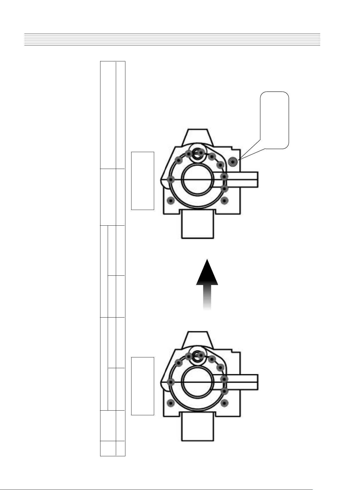
-55-
Service Manual CP-785A
6-1-3. Detail Imformation of Some Component Change of FS-xxT90 (ECN)
(1) FBT Change
- New FBT is electrically compatable for FS-xxT90,xxV81 and PF51T30
ˉ
- But, New FBT have additional pin for FOCUS Ground
- So, New FBT is not inserted in the Old PCB 4859804393
Loc. Part Name
Before the Change After the Change
Applying Date Remark
Part Code Part Description Part Code Part Description
T402 FBT 50H0000181 1352.5008E 50H0000247 FFA64028L From New PCB New FBT do not inserted in the old PCB
Old FBT
(1352.5008E)
New FBT
(RRA64028L)
Additional Hole
(FOCUS GND)

-56-
Service Manual CP-785A
(2) DY Connector Change
- New DY connector (4pin type) will be applied form New PCB
- All of Electronic characteristic is same
Loc. Part Name
Before the Change After the Change
Applying Date Remark
Part Code Part Description Part Code Part Description
V901 CRT 4859633867 A68KTB359X010(B) M50 4859633769 A68KTB359X001(B) M50 DY connector (in the CRT) &
4859629569 A59KPR84X02(D) M50 4859629069 A59KPR84X01(D) M50 From New PCB DY Wafer (in the Main PCB)
P402 CONN WAFER 4859240120 YFW500-06 ************** Delete ************** will be change at the same time
N401,402,403,404
TERM PIN ************** Add ************** 4857417500 DA-IB0214(D2.3/DY PIN)
Comparison
- DY connector : 6 pin type - DY connector : 4 pin type
- P402 is used” - N401~404 are used
- If new PCB apply to Old CRT set : Replace the P401 wafer of old PCB to the New PCB P401
- If new CRT apply to old PCB set : Change the New CRT’s DY connecto to old set’s DY connector
6 pin
DY
Connector
New PCB
4859806493
(FS-xxV81)
Old PCB
4859804393
(FS-xxT81)
4 pin
DY
Connector
Old CRTs
A59KPR84X02
A68KTB359X010
DY wafer : YFW500-06
New CRTs
A59KPR84X01
A68KTB359X001
DY wafer : 4pin Terminal
Red (Hin)
Blue (Hout)
Yellow (Vout)
Green (Vin)
Red (Hin)
Blue (Hout)
Yellow (Vout)
Green (Vin)
PCB Hole & Pattern for DY connentor
4 pin Type DY : available
6 pin Type DY : available
4 pin Type DY : Impossible
6 pin Type DY : available

-57-
Service Manual CP-785A
(3) CRT Ground Net Change
- New CRT GND Net (1pin type) will be applied form New PCB
- New CRT GND Net (1pin type) do not need P904
Before (old CRT Ground Net) New CRT Ground Net
CRT Ground NET
29 inch : 2901H-1015-2P (48519A4210) 29 inch : 2901S-1015-1P (48519A6410)
25 inch : 2501H-1015-2P (48519A4010) 25 inch : 2501S-1015-1P (48519A6310)
P904 (Wafer) YPW500-02 (4859238620) **************Delete **************
Applied Models Current FS-xxT90 (FS-8002)
ˈ
FS-xxV81, FS-xxT90 will be appled
ˉ
old CRT Ground Net ==> Inserted to P904 new CRT Ground Net ==> Inserted to SCT Socket (SCT1)
Connection
- New CRT GND Net (1pin type) will be applied form New PCB
- If old PCB apply to New set : No Problem
- If New PCB apply to old set
a. Method 1 : Replace the P904(Wafer) of old set to P904 of the New PCB
b. Method 2 : Change the wire of old CRT GND NET looks like New CRT GND Net and use it
P904
P904
CRT
GND
SCREEN
FOCUS
GND

-58-
Service Manual CP-785A
(4) Others
- These Technical Changes are applied from New PCB
No.
Changing
Loc. Part Name
Before the Change After the Change
Remark
Item Part Code Part Description Part Code Part Description
Error Amp I806 IC ERROR AMP 1SE130N--- SE130N 1DP142---- DP142
Change Error Amp of Main B+(142V)
1
Change R823 R CARBON FILM RD-4Z512J- 1/4 5.1K OHM J RD-4Z331J- 1/4 330 OHM J
- SE130N : R823 must be 5.1K ohm for 142V
- DP142 & SE140N : R823 must be 330 ohm for 142V
H-Drive Q402 TR T2SD1207T- 2SD1207-T TKTC3229-- KTC3229
KTC3229 : available both old & New PCB
2
Resister R406 R M-OXIDE FILM RS02Z561JS 2W 560 OHM J s RS02Z271JS 2W 270 OHM J S
- If R406=560 ohm (old PCB) then both 2SD1207 & KTC3229 are available
- If R406=270 ohm (new PCB) then KTC3229 are available
No.1 : For more high sensitivity of Main B+ feedback (by reducing of R823)
No.2 : For more small operating temperature of Q401 (by reducing of R406, H-drirve Bias voltage increasing)
-59-
Service Manual CP-785A
-59-
Service Manual CP-785A
Ass’y LOC PART NAME 29 inch (FS-68xxx) 25 inch (FS-59xxx)
PART CODE PART Description PART CODE PART Description
COVER BACK ZZ120 COVER BACK AS PTBCSHD393 DTE-29G5TH PTBCSHD392 DTE-25G5THS
PTBCSHD634 DTE-29G4ZH PTBCSHD635 DTE-25G4ZH
MASK FRONT ZZ200 MASK FRONT AS PTFMSJD393 DTE-29G5TH PTFMSJD392 DTE-25G5THS
PTFMSJD634 DTE-29G4ZH PTFMSJD635 DTE-25G4ZH
CRT ZZ131 CRT GROUND NET 48519A4210 2901H-1015-2P 48519A4010 2501H-1015-2P - xx01H-1015-2P : 2pin Connector
48519A6410 2902S-1015-1P 48519A6310 2502S-1015-1P - xx02S-1015-1P : 1pin Connector
ZZ132 COIL DEGAUSSING 58G0000145 DC-29S2 58G0000144 DC-25S2
V901 CRT 4859633867 A68KTB359X010(B) M50 4859629569 A59KPR84X02(D) M50
- A68...X010, A59...X02 : 6pin DY Connector
4859633769 A68KTB359X001(B) M50 4859629069 A59KPR84X01(D)M50
- A68...X001, A59...X01 : 4pin DY Connector
MAIN PCB C402 C MYLAR CMYH3C123J 1.6KV BUP 0.012MF J CMYH3C912J 1.6KV BUP 9100PF J Retrace Cap.
C404 C MYLAR CMYH3C722J 1.6KV BUP 7200PF J CMYH3C692J 1.6KV BUP 6900PF J Retrace Cap.
C408 C MYLAR CMYE2G624J 400V PU 0.62MF J CMYE2G434J 400V PU 0.43MF J S-Cap.
L401 COIL H-LINEARITY 58H0000065 TRL-140D 58H0000025 TRL-330 H-Linearity Coil
R350 R METAL FILM RN-4Z1501F 1/4 1.50K OHM F RN-4Z1801F 1/4 1.80K OHM F Vertical Def.
R351 R METAL FILM RN-4Z1501F 1/4 1.50K OHM F RN-4Z1801F 1/4 1.80K OHM F Vertical Def.
R556 R CARBON FILM RD-AZ472J- 1/6 4.7K OHM J RD-AZ512J- 1/6 5.1K OHM J ABL
R808 R CARBON FILM RD-4Z911J- 1/4W 910 OHM J RD-4Z102J- 1/4W 1K OHM J OCP
R920 R M-OXIDE FILM RS01Z569J- 1W 5.6 OHM J (TAPPING) RS01Z249J- 1W 2.4 OHM J (TAPPING) Heater
Models - DTE-29xxxx Seriese - DTE-25xxxx Seriese
- FS-68T90,68V81” - FS-59T90,59V81
6-2. Differnce Parts for CRT

-60-
Service Manual CP-785A
Ass’y LOC PART NAME xxG5TH (FS-xxT90) xxG4ZH (FS-xxV81) Remark
PART CODE PART Description PART CODE PART Description
Accessory ZZ100 TRANSMITTER REMOCON 48B4744N08 R-44N08 (AA) 48B4744N09 R-44N09 (AA) - With Text & Without Text
00030 CABLE SCART 4859000160 S-RCA 3P/DIN 4P(1.2M) ********* Not Used ********** - FS-xxT90 Support SVHS (Scart Jack)
COVER BACK ZZ120 COVER BACK AS PTBCSHD393 DTE-29G5TH PTBCSHD634 DTE-29G4ZH
PTBCSHD392 DTE-25G5TH PTBCSHD635 DTE-25G4ZH
MASK FRONT ZZ200 MASK FRONT AS PTFMSJD393 DTE-29G5TH PTFMSJD634 DTE-29G4ZH
PTFMSJD392 DTE-25G5TH PTFMSJD635 DTE-25G4ZH
SPEAKER SP01 SPEAKER 4858310810 F2250C-2141 48A8304800 SS-78128F04 10W 8 OHM
Assembly SP02 SPEAKER 4858310810 F2250C-2141 - - - depends on Cabinet Structure
P601A CONNECTOR 4850704S31
YH025-04+YRT205+ULW800400
- -
MAIN PCB I501 IC MICOM 1DW3653CH1 DW9365/N2/3-CH1 1TDA9385N2 TDA9385PS/N2/3I - With Text & Without Text
Assembly I601 IC AUDIO 1MSP3415D- MSP3415D 1MSP3465V3 MSP3465G-PP-B8-V3 - Stereo & Mono
JA01 WIRE COPPER ********* Deleted ********** 85801065GY AWG22 1/0.65
JJA03 WIRE COPPER ********* Deleted ********** 85801065GY AWG22 1/0.65
JA02 WIRE COPPER 85801065GY AWG22 1/0.65 ********* Deleted ********** - Depends on RCA output Jack
JA04 WIRE COPPER 85801065GY AWG22 1/0.65 ********* Deleted **********
JPA1 JACK PIN BOARD 4859110050 PH-JB-9614D 4859109250 PH-JB-9614A
JPA2 SOCKET RGB 4859200401 YRS21-R1 4859110950 YS01-0001 - FS-xxT90 use Scart Jack for Input-1
D100 LED DSD50RH51B SD50-RH51BGRW ******* In the Control PCB *******
D100M HOLDER LED 4853533600 P.P BK ******* In the Control PCB *******
HP01 JACK EARPHONE 4859102130 YSC-1537 ******* In the Control PCB *******
I703 IC PREAMP 1TS0P1238W TS0P1238WI1 ******* In the Control PCB *******
JPA3 JACK PIN BOARD 4859108450 YSC03P-4120-14A ******* In the Control PCB *******
SW700 SW TACT 5S50101090 THVH472GCA ******* In the Control PCB *******
SW701 SW TACT 5S50101090 THVH472GCA ******* In the Control PCB *******
SW702 SW TACT 5S50101090 THVH472GCA ******* In the Control PCB ******* - depends on Cabinet Structure
SW703 SW TACT 5S50101090 THVH472GCA ******* In the Control PCB *******
SW704 SW TACT 5S50101090 THVH472GCA ******* In the Control PCB *******
SW801 SW POWER PUSH 5S40101143 PS3-22SP (P.C.B) ******* In the Control PCB *******
N005 TERM PIN ********* Deleted ********** 4857417500 DA-IB0214(D2.3/DY PIN)
N006 TERM PIN ********* Deleted ********** 4857417500 DA-IB0214(D2.3/DY PIN)
P602 CONN WAFER ********* Not Used ********** 485923522S YW025-09 (STICK)
P701 CONN WAFER ********* Not Used ********** 485923192S YW025-06 (STICK)
CONTROL
ZZ230 PCB CONTROL AS ********* Not Used ********** PTCTSWD634 DTE-29G4ZH - depends on Cabinet Structure
PCB
6-3. Function & Cabinet Different Parts List
* These different Pars are available only New PCB (4859806493)
* The old PCB (4859804393) did not support FS-xxV81 serease

-61-
Service Manual CP-785A
LOC PART NAME PART Code PART Description Remark
6-4. All Electrical Parts List
6-4-1. Old Main PCB Assembly Parts List (for old FS-xxT90 Models)
- The old Main Assembly will be changed. (October 2002)
- This old PCB do not support FS-xxV81 Models
A001 PCB MAIN 4859804393 330X246 S1L
C101 C ELECTRO CEXF1H100V 50V RSS 10MF (5X11) TP
C102 C ELECTRO CEXF1H470V 50V RSS 47MF (6.3X11) TP
C103 C CERA CCZB1H102K 50V B 1000PF K (AXIAL)
C104 C CERA CCXB1H102K 50V B 1000PF K (TAPPING)
C106 C ELECTRO CEXF1C221V 16V RSS 220MF (8X11.5) TP
C108 C CERA CCZB1H101K 50V B 100PF K (AXIAL)
C110 C CERA CCZB1H102K 50V B 1000PF K (AXIAL)
C120 C CERA CCZB1H102K 50V B 1000PF K (AXIAL)
C121 C ELECTRO CEXF1H100V 50V RSS 10MF (5X11) TP
C305 C ELECTRO CEXF1E471V 25V RSS 470MF (10X16) TP
C313 C MYLAR CMXM2A104J 100V 0.1MF J (TP)
C315 C ELECTRO CEXF2C470C 160V RUS 47MF (13X25) TP
C320 C CERA SEMI CBXF1H104Z 50V F 0.1MF Z (TAPPING)
C350 C CERA CCXF1H473Z 50V F 0.047MF Z (TAPPING)
C351 C CERA CCXF1H473Z 50V F 0.047MF Z (TAPPING)
C370 C MYLAR CMXM2A473J 100V 0.047MF J (TP)
C401 C ELECTRO CEXF1H100C 50V RUS 10MF (5X11) TP
C402 C MYLAR CMYH3C123J 1.6KV BUP 0.012MF J 29 inch
C MYLAR CMYH3C912J 1.6KV BUP 9100PF J 25 inch
C404 C MYLAR CMYH3C722J 1.6KV BUP 7200PF J 29 inch
C MYLAR CMYH3C692J 1.6KV BUP 6900PF J 25 inch
C408 C MYLAR CMYE2G624J 400V PU 0.62MF J 29 inch
C MYLAR CMYE2G434J 400V PU 0.43MF J 25 inch
C412 C ELECTRO CEXF2C339C 160V RUS 3.3MF (8X11.5) TP
C414 C MYLAR CMXM2A104J 100V 0.1MF J (TP)
C415 C ELECTRO CEXF2E479V 250V RSS 4.7MF (10X16)TP
C418 C CERA CCXB1H102K 50V B 1000PF K (TAPPING)
C420 C CERA CCXB2H222K 500V B 2200PF K (TAPPING)
C430 C MYLAR CMYH3C122J 1.6KV BUP 1200PF J
C431 C MYLAR CMXE2D103J 200V PU 0.01MF J (TP)
C440 C MYLAR CMXE2G273J 400V PU 0.027MF J (TP)
C499 C ELECTRO CEYD1H689W 50V RHD 6.8MF (16X35.5)
C509 C ELECTRO CEXF1E470V 25V RSS 47MF (5X11) TP
C511 C MYLAR CMXM2A224J 100V 0.22MF J
C512 C MYLAR CMXM2A224J 100V 0.22MF J
C513 C CERA SEMI CBZF1H104Z 50V F 0.1MF Z
C514 C ELECTRO CEXF1E101V 25V RSS 100MF (6.3X11) TP
C515 C CERA CBZR1C222M 16V Y5R 2200PF M (AXIAL)
C516 C CERA CBZR1C472M 16V Y5R 4700PF M (AXIAL)
C517 C ELECTRO CEXF1H109V 50V RSS 1MF (5X11) TP
C518 C CERA SEMI CBZF1H104Z 50V F 0.1MF Z
C519 C ELECTRO CEXF1H109V 50V RSS 1MF (5X11) TP

-62-
Service Manual CP-785A
LOC PART NAME PART Code PART Description Remark
C520 C CERA CCZB1H102K 50V B 1000PF K (AXIAL)
C521 C CERA CCZB1H102K 50V B 1000PF K (AXIAL)
C523 C CERA SEMI CBZF1H104Z 50V F 0.1MF Z
C524 C MYLAR CMXL1J104J 63V MEU 0.1MF J
C525 C CERA CCXB1H102K 50V B 1000PF K (TAPPING)
C526 C MYLAR CMXL1J104J 63V MEU 0.1MF J
C527 C MYLAR CMXM2A473J 100V 0.047MF J (TP)
C528 C ELECTRO CEXF1E101V 25V RSS 100MF (6.3X11) TP
C529 C CERA SEMI CBZF1H104Z 50V F 0.1MF Z
C530 C ELECTRO CEXF1E101V 25V RSS 100MF (6.3X11) TP
C531 C CERA CCXF1H473Z 50V F 0.047MF Z (TAPPING)
C532 C ELECTRO CEXF1H100V 50V RSS 10MF (5X11) TP
C533 C CERA CCZB1H102K 50V B 1000PF K (AXIAL)
C534 C CERA CCZF1H223Z 50V F 0.022MF Z
C535 C CERA CCZF1H223Z 50V F 0.022MF Z
C536 C CERA CCZF1H223Z 50V F 0.022MF Z
C537 C CERA SEMI CBXF1H104Z 50V F 0.1MF Z (TAPPING)
C540 C ELECTRO CEXF1H220V 50V RSS 22MF (5X11) TP
C541 C ELECTRO CEXF1H220V 50V RSS 22MF (5X11) TP
C542 C ELECTRO CEXF1H100V 50V RSS 10MF (5X11) TP
C543 C ELECTRO CEXF1H100V 50V RSS 10MF (5X11) TP
C550 C ELECTRO CEXF1H229V 50V RSS 2.2MF (5X11) TP
C555 C ELECTRO CEXF1C470V 16V RSS 47MF (5X11) TP
C560 C CERA SEMI CBXF1H104Z 50V F 0.1MF Z (TAPPING)
C561 C ELECTRO CEXF1E101V 25V RSS 100MF (6.3X11) TP
C564 C ELECTRO CEXF1E101V 25V RSS 100MF (6.3X11) TP
C565 C CERA SEMI CBXF1H104Z 50V F 0.1MF Z (TAPPING)
C577 C CERA CCZB1H561K 50V B 560PF K
C585 C CERA CCXB1H222K 50V B 2200PF K (TAPPING)
C590 C CERA CXCH1H270J 50V CH 27PF J (TAPPING)
C591 C CERA CXCH1H270J 50V CH 27PF J (TAPPING)
C592 C CERA SEMI CBXF1H104Z 50V F 0.1MF Z (TAPPING)
C593 C ELECTRO CEXF1E101V 25V RSS 100MF (6.3X11) TP
C601 C CERA CCXB1H472K 50V B 4700PF K (TAPPING)
C602 C ELECTRO CEXF1H100V 50V RSS 10MF (5X11) TP
C603 C CERA CCXB1H472K 50V B 4700PF K (TAPPING)
C604 C ELECTRO CEXF1E102V 25V RSS 1000MF (13X20) TP
C605 C ELECTRO CEXF1E470V 25V RSS 47MF (5X11) TP
C608 C ELECTRO CEXF1H100V 50V RSS 10MF (5X11) TP
C610 C ELECTRO CEXF1H100V 50V RSS 10MF (5X11) TP
C611 C ELECTRO CEXF1H339V 50V RSS 3.3MF (5X11) TP
C612 C ELECTRO CEXF1H109V 50V RSS 1MF (5X11) TP
C613 C ELECTRO CEXF1H109V 50V RSS 1MF (5X11) TP
C614 C ELECTRO CEXF1H109V 50V RSS 1MF (5X11) TP
C615 C ELECTRO CEXF1H109V 50V RSS 1MF (5X11) TP
C616 C ELECTRO CEXF1H100V 50V RSS 10MF (5X11) TP

-63-
Service Manual CP-785A
LOC PART NAME PART Code PART Description Remark
C617 C CERA SEMI CBXF1H104Z 50V F 0.1MF Z (TAPPING)
C618 C ELECTRO CEXF1C470V 16V RSS 47MF (5X11) TP
C620 C CERA CXCH1H509D 50V CH 5PF D (TAPPING)
C621 C CERA CXCH1H509D 50V CH 5PF D (TAPPING)
C622 C CERA CCXF1H223Z 50V F 0.022MF Z (TAPPING)
C625 C ELECTRO CEXF1H479V 50V RSS 4.7MF (5X11) TP
C626 C ELECTRO CEXF1H479V 50V RSS 4.7MF (5X11) TP
C629 C CERA SEMI CBXF1H104Z 50V F 0.1MF Z (TAPPING)
C630 C ELECTRO CEXF1E470V 25V RSS 47MF (5X11) TP
C631 C CERA SEMI CBXF1H104Z 50V F 0.1MF Z (TAPPING)
C635 C CERA SEMI CBXF1H104Z 50V F 0.1MF Z (TAPPING)
C636 C ELECTRO CEXF1H220V 50V RSS 22MF (5X11) TP
C650 C CERA CZSL1H470J 50V SL 47PF J (AXIAL)
C660 C ELECTRO CEXF1H100V 50V RSS 10MF (5X11) TP
C661 C MYLAR CMXM2A224J 100V 0.22MF J
C662 C MYLAR CMXM2A224J 100V 0.22MF J
C665 C CERA CCXB1H472K 50V B 4700PF K (TAPPING)
C666 C CERA SEMI CBXF1H104Z 50V F 0.1MF Z (TAPPING)
C667 C CERA CCXB1H472K 50V B 4700PF K (TAPPING)
C668 C MYLAR CMXM2A224J 100V 0.22MF J
C669 C MYLAR CMXM2A224J 100V 0.22MF J
C690 C ELECTRO CEXF1H479V 50V RSS 4.7MF (5X11) TP
C691 C ELECTRO CEXF1H479V 50V RSS 4.7MF (5X11) TP
C698 C CERA CZSL1H470J 50V SL 47PF J (AXIAL)
C699 C CERA CZSL1H470J 50V SL 47PF J (AXIAL)
C770 C ELECTRO CEXF1E101V 25V RSS 100MF (6.3X11) TP
C771 C CERA SEMI CBZF1H104Z 50V F 0.1MF Z
C801 C LINE ACROSS CL1UC3474M 0.47MF 1J(UCVSNDF/SV)+Q/O (!)
C803 C CERA CCXB3A472K 1KV B 4700PF K (TAPPING)
C804 C CERA CCXB3A472K 1KV B 4700PF K (TAPPING)
C805 C ELECTRO CEYN2W151P 450V LHS 150MF (25X40)
C806 C ELECTRO CEXF1H330V 50V RSS 33MF (6.3X11) TP
C807 C CERA CCXF1H473Z 50V F 0.047MF Z (TAPPING)
C808 C ELECTRO CEXF1H479V 50V RSS 4.7MF (5X11) TP
C809 C CERA CCZB1H102K 50V B 1000PF K (AXIAL)
C810 C CERA SEMI CBXB3D102K 2KV BL(N) 1000PF K (T)
C812 C CERA AC CH1AFE472M 4KV 4700PF M KX DE1610 (!)
C813 C ELECTRO CEYF2D101V 200V RSS 100MF (16X31.5)
C814 C ELECTRO CEXF2E470V 250V RSS 47MF (16X25) TP
C820 C CERA CCYR3A471K 1KV R 470PF K 125 DE0705
C821 C CERA CCXB1H102K 50V B 1000PF K (TAPPING)
C823 C ELECTRO CEXF1E102V 25V RSS 1000MF (13X20) TP
C824 C CERA CCXB3A471K 1KV B 470PF K (T)
C830 C CERA SEMI CBZF1H104Z 50V F 0.1MF Z
C831 C CERA CCXB3A471K 1KV B 470PF K (T)
C832 C ELECTRO CEXF1E102V 25V RSS 1000MF (13X20) TP

-64-
Service Manual CP-785A
LOC PART NAME PART Code PART Description Remark
C835 C ELECTRO CEXF1H470V 50V RSS 47MF (6.3X11) TP
C840 C ELECTRO CEXF1C222V 16V RSS 2200MF (16X31.5) TP
C841 C ELECTRO CEXF1C222V 16V RSS 2200MF (16X31.5) TP
C844 C ELECTRO CEXF1E101V 25V RSS 100MF (6.3X11) TP
C850 C CERA CCXB1H152K 50V B 1500PF K (TAPPING)
C861 C ELECTRO CEXF1E102V 25V RSS 1000MF (13X20) TP
C863 C ELECTRO CEXF1E101V 25V RSS 100MF (6.3X11) TP
C866 C CERA CCXB3A471K 1KV B 470PF K (T)
C888 C ELECTRO CEXF1C470V 16V RSS 47MF (5X11) TP
C905 C ELECTRO CEXF2E479V 250V RSS 4.7MF (10X16)TP
C906 C ELECTRO CEXF2E100V 250V RSS 10MF (10X20) TP
C965 C CERA SEMI CBXB3D102K 2KV BL(N) 1000PF K (T)
C968 C MYLAR CMXL2E104K 250V MEU 0.1MF K
CA13 C CERA CCXB1H271K 50V B 270PF K (TAPPING)
CA14 C CERA CCXB1H271K 50V B 270PF K (TAPPING)
D100 LED DSD50RH51B SD50-RH51BGRW
D100M HOLDER LED 4853533600 P.P BK
D101 DIODE D1N4148--- 1N4148 (TAPPING)
D102 DIODE D1SS85TA-- 1SS85TA
D313 DIODE DRGP15J--- RGP15J
D360 DIODE ZENER DMTZJ22D-- MTZJ 22D
D361 DIODE ZENER DUZ33B---- UZ-33B
D367 DIODE ZENER DUZ33B---- UZ-33B
D381 DIODE ZENER DUZ33B---- UZ-33B
D403 DIODE DDG3------ DG3
D404 DIODE DRGP30J--- RGP30J
D405 DIODE DRGP15J--- RGP15J
D407 DIODE DRGP15J--- RGP15J
D408 DIODE DRGP15J--- RGP15J
D410 DIODE D1N4004S-- 1N4004S
D411 DIODE D1N4004S-- 1N4004S
D414 DIODE D1N4004S-- 1N4004S
D450 DIODE DRGP15J--- RGP15J
D520 DIODE D1N4148--- 1N4148 (TAPPING)
D521 DIODE D1N4148--- 1N4148 (TAPPING)
D601 DIODE D1N4148--- 1N4148 (TAPPING)
D602 DIODE D1N4148--- 1N4148 (TAPPING)
D710 DIODE ZENER DMTZJ5R1A- MTZJ 5.1A
D801 DIODE DLT2A05G-- LT2A05G (TP)
D802 DIODE DLT2A05G-- LT2A05G (TP)
D803 DIODE DLT2A05G-- LT2A05G (TP)
D804 DIODE DLT2A05G-- LT2A05G (TP)
D805 DIODE DRGP15J--- RGP15J
D806 DIODE DRGP15J--- RGP15J
D808 DIODE DRGP15J--- RGP15J
D809 DIODE DRGP15J--- RGP15J

-65-
Service Manual CP-785A
LOC PART NAME PART Code PART Description Remark
D810 DIODE DRGP15J--- RGP15J
D811 DIODE ZENER DMTZJ5R6B- MTZJ 5.6B
D820 DIODE DRGP30J--- RGP30J
D821 DIODE DRGP15J--- RGP15J
D822 DIODE ZENER DMTZJ9R1C- MTZJ 9.1C
D824 DIODE D1N4148--- 1N4148 (TAPPING)
D825 DIODE D1N4148--- 1N4148 (TAPPING)
D830 DIODE DRGP15J--- RGP15J
D831 DIODE DRGP15J--- RGP15J
D840 DIODE D1N4148--- 1N4148 (TAPPING)
D841 DIODE D1N4148--- 1N4148 (TAPPING)
D860 DIODE DRGP30J--- RGP30J
D904 DIODE D1N4004S-- 1N4004S
D905 DIODE D1N4004S-- 1N4004S
D906 DIODE D1N4004S-- 1N4004S
D907 DIODE D1N4937G-- 1N4937G (TAPPING)
DA02 DIODE ZENER DMTZJ5R6B- MTZJ 5.6B
DA04 DIODE ZENER DMTZJ5R6B- MTZJ 5.6B
DA11 DIODE ZENER DMTZJ5R6B- MTZJ 5.6B
DA15 DIODE ZENER DMTZJ5R6B- MTZJ 5.6B
DA16 DIODE ZENER DMTZJ5R6B- MTZJ 5.6B
DA20 DIODE ZENER DMTZJ5R6B- MTZJ 5.6B
F801 FUSE GLASS TUBE 5FSGB4022L SEMKO TL 4A 250V MF51 (!)
F801A CLIP FUSE 4857415001 PFC5000-0702
F801B CLIP FUSE 4857415001 PFC5000-0702
G900 SPARK GAP 4SG0DX0001 SSG-102-A1(1.0KV) TAP
G901 SPARK GAP 4SG0DX0001 SSG-102-A1(1.0KV) TAP
G902 SPARK GAP 4SG0DX0001 SSG-102-A1(1.0KV) TAP
G903 SPARK GAP 4SG0DX0001 SSG-102-A1(1.0KV) TAP
HP01 JACK EARPHONE 4859102130 YSC-1537
I301 HEAT SINK ASS`Y PTC2SW8217 1TDA8358J- + 7174301011
I501 IC MICOM 1DW3653CH1 DW9365/N2/3-CH1
I601 IC AUDIO 1MSP3415D- MSP3415D
I602 HEAT SINK ASS`Y PTA2SW8215 1TDA8946J- + 7174301011
I702 IC 1AT24C08PC AT24C08-10PC
I703 IC PREAMP 1TS0P1238W TS0P1238WI1
I801 HEAT SINK ASS`Y PTA2SW7910 1STRF6654- + 7174301211
I804 IC PHOTO COUPLER 1KP1010C-- KP-1010C
I805 IC 1UPC574J-- UPC574J
I806 IC 1SE130N--- SE130N DP142,SE140N
==> R823 Must be 330 ohm
ˉ
I810 THYRISTOR TX0202DA-- X0202DA1BA2
I820 IC REGULATOR 1KA7805--- KA7805
I822 IC REGULATOR 1KA7808--- KA7808
I823 IC REGULATOR 1LP295033- LP2950 3.3V
I901 IC VIDEO AMP 1TDA6107Q- TDA6107Q

-66-
Service Manual CP-785A
LOC PART NAME PART Code PART Description Remark
JPA1 JACK PIN BOARD 4859110050 PH-JB-9614D
JPA2 SOCKET RGB 4859200401 YRS21-R1
JPA3 JACK PIN BOARD 4859108450 YSC03P-4120-14A
L101 COIL PEAKING 5CPZ100K02 10UH K (AXIAL 3.5MM)
L350 COIL PEAKING 5CPZ109M04 1UH 10.5MM M (LAL04TB)
L381 COIL PEAKING 5CPZ109M04 1UH 10.5MM M (LAL04TB)
L401 COIL H-LINEARITY 58H0000065 TRL-140D 29 inch
COIL H-LINEARITY 58H0000025 TRL-330 25 inch
L402 COIL CHOKE 58C7070085 TLN-3062A
L500 COIL PEAKING 5CPZ120K02 12UH K (AXIAL 3.5MM)
L501 COIL PEAKING 5CPZ100K02 10UH K (AXIAL 3.5MM)
L502 COIL PEAKING 5CPZ100K02 10UH K (AXIAL 3.5MM)
L510 COIL PEAKING 5CPZ100K02 10UH K (AXIAL 3.5MM)
L511 COIL PEAKING 5CPZ100K02 10UH K (AXIAL 3.5MM)
L512 COIL PEAKING 5CPZ100K02 10UH K (AXIAL 3.5MM)
L601 COIL PEAKING 5CPZ479K02 4.7UH K (AXIAL 3.5MM)
L602 COIL PEAKING 5CPZ479K02 4.7UH K (AXIAL 3.5MM)
L603 COIL PEAKING 5CPZ479K02 4.7UH K (AXIAL 3.5MM)
L650 COIL BEAD 5MC0000100 HC-3550
L801 COIL BEAD 5MC0000100 HC-3550
L802 COIL CHOKE 58CX430599 AZ-9004Y 940K TP
L803 COIL BEAD 5MC0000100 HC-3550
LF801 FILTER LINE 5PLF24A1-- LF-24A1
N001 TERM PIN 4857417500 DA-IB0214(D2.3/DY PIN)
N002 TERM PIN 4857417500 DA-IB0214(D2.3/DY PIN)
N003 TERM PIN 4857417500 DA-IB0214(D2.3/DY PIN)
N004 TERM PIN 4857417500 DA-IB0214(D2.3/DY PIN)
P401 CONNECTOR 4850705N19 YBNH250+YBNT250+ULW=400
P402 CONN WAFER 4859240120 YFW500-06
P501 CONNECTOR 4850705N14 YBNH250-05+YBNH250+ULW500
P601 CONN WAFER 485923172S YW025-04 (STICK)
P904 CONN WAFER 4859238620 YPW500-02
PWC1 CORD POWER AS 4859903010 KKP560+BL102NG+TUBE=2600
Q101 TR TKTC3198Y- KTC3198Y
Q103 TR TKTC3202Y- KTC3202Y (TP)
Q401 TR TST2009DH1 ST2009DH1 COMPATIBLE
T2SD2553-- 2SD-2553
Q402 TR T2SD1207T- 2SD1207-T (TAPPING) COMPATIBLE
TKTC3229-- KTC3229
Q501 TR TKTA1266Y- KTA1266Y (TP)
Q502 TR TKTC3198Y- KTC3198Y
Q503 TR TKTC3198Y- KTC3198Y
Q504 TR TKTC3198Y- KTC3198Y
Q505 TR TKTC3198Y- KTC3198Y
Q508 TR TKTC3198Y- KTC3198Y
Q601 TR TKTA1266Y- KTA1266Y (TP)

-67-
Service Manual CP-785A
LOC PART NAME PART Code PART Description Remark
Q807 TR TKTC3198Y- KTC3198Y
Q808 TR TKTC3198Y- KTC3198Y
Q809 TR TKTC3198Y- KTC3198Y
Q810 TR TKTC3198Y- KTC3198Y
Q811 TR TKTC3198Y- KTC3198Y
R101 R CARBON FILM RD-AZ473J- 1/6 47K OHM J
R102 R CARBON FILM RD-AZ472J- 1/6 4.7K OHM J
R103 R CARBON FILM RD-AZ123J- 1/6 12K OHM J
R104 R CARBON FILM RD-AZ104J- 1/6 100K OHM J
R105 R CARBON FILM RD-AZ392J- 1/6 3.9K OHM J
R106 R CARBON FILM RD-AZ101J- 1/6 100 OHM J
R107 R CARBON FILM RD-AZ101J- 1/6 100 OHM J
R113 R CARBON FILM RD-AZ562J- 1/6 5.6K OHM J
R114 R CARBON FILM RD-AZ562J- 1/6 5.6K OHM J
R115 R CARBON FILM RD-AZ682J- 1/6 6.8K OHM J
R116 R CARBON FILM RD-AZ222J- 1/6 2.2K OHM J
R117 R CARBON FILM RD-AZ222J- 1/6 2.2K OHM J
R120 R CARBON FILM RD-AZ101J- 1/6 100 OHM J
R310 R CARBON FILM RD-AZ102J- 1/6 1K OHM J
R311 R CARBON FILM RD-AZ102J- 1/6 1K OHM J
R331 R M-OXIDE FILM RS01Z331J- 1W 330 OHM J (TAPPING)
R340 R CARBON FILM RD-4Z473J- 1/4 47K OHM J
R350 R METAL FILM RN-4Z1501F 1/4 1.50K OHM F 29 inch
R METAL FILM RN-4Z1801F 1/4 1.80K OHM F 25 inch
R351 R METAL FILM RN-4Z1501F 1/4 1.50K OHM F 29 inch
R METAL FILM RN-4Z1801F 1/4 1.80K OHM F 25 inch
R370 R CARBON FILM RD-4Z159J- 1/4 1.5 OHM J
R394 R CARBON FILM RD-AZ272J- 1/6 2.7K OHM J
R395 R CARBON FILM RD-AZ824J- 1/6 820K OHM J
R396 R CARBON FILM RD-AZ272J- 1/6 2.7K OHM J
R397 R CARBON FILM RD-AZ823J- 1/6 82K OHM J
R398 R FUSIBLE RF01Z828JA 1W 0.82 OHM J A CURVE
R399 R M-OXIDE FILM RS02Z120JS 2W 12 OHM J SMALL
R401 R CARBON FILM RD-4Z272J- 1/4 2.7K OHM J
R402 R CARBON FILM RD-4Z220J- 1/4 22 OHM J
R404 R CARBON FILM RD-4Z399J- 1/4 3.9 OHM J
R406 R M-OXIDE FILM RS02Z561JS 2W 560 OHM J SMALL
R415 R M-OXIDE FILM RS02Z102JS 2W 1K OHM J SMALL
R420 R CARBON FILM RD-AZ223J- 1/6 22K OHM J
R427 R M-OXIDE FILM RS01Z101J- 1W 100 OHM J (TAPPING)
R450 R M-OXIDE FILM RS02Z223JS 2W 22K OHM J SMALL
R501 R CARBON FILM RD-AZ101J- 1/6 100 OHM J
R502 R CARBON FILM RD-AZ101J- 1/6 100 OHM J
R503 R CARBON FILM RD-AZ332J- 1/6 3.3K OHM J
R504 R CARBON FILM RD-AZ101J- 1/6 100 OHM J
R505 R CARBON FILM RD-AZ101J- 1/6 100 OHM J

-68-
Service Manual CP-785A
LOC PART NAME PART Code PART Description Remark
R506 R CARBON FILM RD-AZ332J- 1/6 3.3K OHM J
R507 R CARBON FILM RD-AZ101J- 1/6 100 OHM J
R508 R CARBON FILM RD-AZ332J- 1/6 3.3K OHM J
R509 R CARBON FILM RD-AZ681J- 1/6 680 OHM J
R512 R CARBON FILM RD-AZ101J- 1/6 100 OHM J
R513 R CARBON FILM RD-AZ101J- 1/6 100 OHM J
R514 R CARBON FILM RD-AZ101J- 1/6 100 OHM J
R515 R CARBON FILM RD-AZ153J- 1/6 15K OHM J
R516 R CARBON FILM RD-AZ393J- 1/6 39K OHM J
R517 R CARBON FILM RD-AZ181J- 1/6 180 OHM J
R518 R CARBON FILM RD-AZ273J- 1/6 27K OHM J
R520 R CARBON FILM RD-AZ333J- 1/6 33K OHM J
R521 R CARBON FILM RD-AZ391J- 1/6 390 OHM J
R522 R CARBON FILM RD-AZ221J- 1/6 220 OHM J
R523 R CARBON FILM RD-AZ331J- 1/6 330 OHM J
R524 R CARBON FILM RD-AZ561J- 1/6 560 OHM J
R525 R CARBON FILM RD-AZ104J- 1/6 100K OHM J
R526 R CARBON FILM RD-AZ479J- 1/6 4.7 OHM J
R527 R CARBON FILM RD-AZ431J- 1/6 430 OHM J
R528 R CARBON FILM RD-AZ221J- 1/6 220 OHM J
R530 R CARBON FILM RD-AZ470J- 1/6 47 OHM J
R531 R CARBON FILM RD-AZ102J- 1/6 1K OHM J
R533 R CARBON FILM RD-AZ103J- 1/6 10K OHM J
R537 R CARBON FILM RD-AZ101J- 1/6 100 OHM J
R538 R CARBON FILM RD-AZ101J- 1/6 100 OHM J
R539 R CARBON FILM RD-AZ101J- 1/6 100 OHM J
R540 R CARBON FILM RD-AZ101J- 1/6 100 OHM J
R541 R CARBON FILM RD-AZ101J- 1/6 100 OHM J
R543 R CARBON FILM RD-AZ472J- 1/6 4.7K OHM J
R545 R CARBON FILM RD-AZ682J- 1/6 6.8K OHM J
R547 R CARBON FILM RD-AZ103J- 1/6 10K OHM J
R548 R CARBON FILM RD-AZ472J- 1/6 4.7K OHM J
R549 R CARBON FILM RD-AZ472J- 1/6 4.7K OHM J
R550 R CARBON FILM RD-AZ472J- 1/6 4.7K OHM J
R555 R CARBON FILM RD-AZ103J- 1/6 10K OHM J
R556 R CARBON FILM RD-AZ472J- 1/6 4.7K OHM J 29 inch
R CARBON FILM RD-AZ512J- 1/6 5.1K OHM J 25 inch
R567 R CARBON FILM RD-AZ101J- 1/6 100 OHM J
R570 R CARBON FILM RD-AZ102J- 1/6 1K OHM J
R580 R CARBON FILM RD-AZ561J- 1/6 560 OHM J
R585 R CARBON FILM RD-AZ224J- 1/6 220K OHM J
R586 R CARBON FILM RD-AZ221J- 1/6 220 OHM J
R587 WIRE COPPER 85801065GY AWG22 1/0.65 TIN COATING
R588 WIRE COPPER 85801065GY AWG22 1/0.65 TIN COATING
R589 WIRE COPPER 85801065GY AWG22 1/0.65 TIN COATING
R595 WIRE COPPER 85801065GY AWG22 1/0.65 TIN COATING

-69-
Service Manual CP-785A
LOC PART NAME PART Code PART Description Remark
R597 R METAL FILM RN-4Z1502F 1/4 15K OHM F
R598 R METAL FILM RN-4Z1502F 1/4 15K OHM F
R599 R CARBON FILM RD-AZ101J- 1/6 100 OHM J
R605 R CARBON FILM RD-AZ751J- 1/6 750 OHM J
R606 R CARBON FILM RD-AZ751J- 1/6 750 OHM J
R608 R CARBON FILM RD-2Z151J- 1/2 150 OHM J
R609 R CARBON FILM RD-2Z151J- 1/2 150 OHM J
R610 R CARBON FILM RD-AZ102J- 1/6 1K OHM J
R611 R CARBON FILM RD-AZ104J- 1/6 100K OHM J
R614 R CARBON FILM RD-AZ102J- 1/6 1K OHM J
R615 R CARBON FILM RD-AZ102J- 1/6 1K OHM J
R620 R CARBON FILM RD-AZ102J- 1/6 1K OHM J
R621 R CARBON FILM RD-AZ101J- 1/6 100 OHM J
R622 R CARBON FILM RD-AZ101J- 1/6 100 OHM J
R650 R CARBON FILM RD-AZ822J- 1/6 8.2K OHM J
R660 R CARBON FILM RD-AZ822J- 1/6 8.2K OHM J
R661 R CARBON FILM RD-AZ752J- 1/6 7.5K OHM J
R662 R CARBON FILM RD-AZ752J- 1/6 7.5K OHM J
R700 R CARBON FILM RD-2Z332J- 1/2 3.3K OHM J
R710 R CARBON FILM RD-AZ431J- 1/6 430 OHM J
R711 R CARBON FILM RD-AZ431J- 1/6 430 OHM J
R713 R CARBON FILM RD-AZ331J- 1/6 330 OHM J
R720 R CARBON FILM RD-AZ122J- 1/6 1.2K OHM J
R721 R CARBON FILM RD-AZ181J- 1/6 180 OHM J
R722 R CARBON FILM RD-AZ221J- 1/6 220 OHM J
R723 R CARBON FILM RD-AZ331J- 1/6 330 OHM J
R724 R CARBON FILM RD-AZ471J- 1/6 470 OHM J
R801 POSISTOR DPC7R0M290 2322 662 96709 COMPATIBLE
DDC7R0M290 ECPCD7R0M290
R802 R M-OXIDE FILM RS02Z753JS 2W 75K OHM J SMALL
R803 R M-OXIDE FILM RS02Z473JS 2W 47K OHM J SMALL
R804 R FUSIBLE RF02Z158K- 2W 0.15 OHM K (TAPPING)
R805 R CARBON FILM RD-2Z100J- 1/2 10 OHM J
R806 R CARBON FILM RD-4Z472J- 1/4 4.7K OHM J
R807 R CARBON FILM RD-2Z272J- 1/2 2.7K OHM J
R808 R CARBON FILM RD-4Z911J- 1/4 910 OHM J 29 inch
R CARBON FILM RD-4Z102J- 1/4 1K OHM J 25 inch
R810 R CARBON FILM RD-4Z102J- 1/4 1K OHM J
R811 R CARBON COMP RC-2Z565KP 1/2 5.6M OHM K
R817 R CARBON FILM RD-AZ473J- 1/6 47K OHM J
R819 R CEMENT RX10B339JQ 10W 3.3 OHM J BEN 25MM 4P
R820 R CARBON FILM RD-AZ102J- 1/6 1K OHM J
R821 R CARBON FILM RD-4Z102J- 1/4 1K OHM J
R823 R CARBON FILM RD-4Z331J- 1/4 330 OHM J When I806 is DP142 (or SE140)
R CARBON FILM RD-4Z512J- 1/4 5.1K OHM J When I806 is SE130
R829 R CARBON FILM RD-AZ223J- 1/6 22K OHM J
-70-
Service Manual CP-785A
LOC PART NAME PART Code PART Description Remark
R830 R CARBON FILM RD-AZ332J- 1/6 3.3K OHM J
R840 R CARBON FILM RD-4Z220J- 1/4 22 OHM J
R841 R CARBON FILM RD-2Z479J- 1/2 4.7 OHM J
R850 R CARBON FILM RD-2Z479J- 1/2 4.7 OHM J
R855 R CARBON FILM RD-4Z185J- 1/4 1.8M OHM J
R870 R CARBON FILM RD-2Z222J- 1/2 2.2K OHM J
R888 R CARBON FILM RD-AZ103J- 1/6 10K OHM J
R910 R CARBON FILM RD-AZ101J- 1/6 100 OHM J
R911 R CARBON FILM RD-AZ101J- 1/6 100 OHM J
R912 R CARBON FILM RD-AZ101J- 1/6 100 OHM J
R913 R CARBON COMP RC-2Z102K- 1/2 1K OHM K
R914 R CARBON COMP RC-2Z102K- 1/2 1K OHM K
R915 R CARBON COMP RC-2Z102K- 1/2 1K OHM K
R920 R M-OXIDE FILM RS01Z569J- 1W 5.6 OHM J (TAPPING) 29 inch
R M-OXIDE FILM RS01Z249J- 1W 2.4 OHM J (TAPPING) 25 inch
R921 R CARBON FILM RD-AZ102J- 1/6 1K OHM J
R922 R CARBON FILM RD-AZ102J- 1/6 1K OHM J
R923 R CARBON FILM RD-AZ102J- 1/6 1K OHM J
R924 R CARBON FILM RD-4Z105J- 1/4 1M OHM J
R925 R CARBON FILM RD-4Z102J- 1/4 1K OHM J
RA01 R CARBON FILM RD-AZ680J- 1/6 68 OHM J
RA11 R CARBON FILM RD-AZ680J- 1/6 68 OHM J
RA12 R CARBON FILM RD-AZ680J- 1/6 68 OHM J
RA16 R CARBON FILM RD-AZ680J- 1/6 68 OHM J
RA20 R CARBON FILM RD-AZ473J- 1/6 47K OHM J
RA21 R CARBON FILM RD-AZ473J- 1/6 47K OHM J
RA40 R CARBON FILM RD-AZ102J- 1/6 1K OHM J
RA41 R CARBON FILM RD-AZ102J- 1/6 1K OHM J
SCT1 SOCKET CRT 4859303530 PCS629-03C COMPATIBLE (!)
4859303830 ISMG94S
SF01 FILTER SAW 5PK3953M-- K3953M
SF02 FILTER SAW 5PK9650M-- K9650M
SW700 SW TACT 5S50101090 THVH472GCA
SW701 SW TACT 5S50101090 THVH472GCA
SW702 SW TACT 5S50101090 THVH472GCA
SW703 SW TACT 5S50101090 THVH472GCA
SW704 SW TACT 5S50101090 THVH472GCA
SW801 SW POWER PUSH 5S40101143 PS3-22SP (P.C.B)
T401 TRANS DRIVE 50D19A1--- TD-19A1
T402 FBT (old) 50H0000181 1352.5008E New FBT Needs Additional
FBT (new) 50H0000247 FFA64028L hole ==> Can not be inserted
T801 TRANS SMPS 50M4950A8- TSM-4950A8
U100 TUNER VARACTOR 4859721530 DT5-BF18D N
X502 CRYSTAL QUARTZ 5XE12R000E HC-49/U 12.00000MHZ 30PPM
X601 CRYSTAL QUARTZ 5XE18R432E HC-49/U 18.43200MHZ 30PPM
Z501 FILTER CERA 5PYXT5R5MB XT 5.5MB

-71-
Service Manual CP-785A
LOC PART NAME PART Code PART Description Remark
A001 PCB MAIN 4859806493 330X246 S1B
C101 C ELECTRO CEXF1H100V 50V RSS 10MF (5X11) TP
C102 C ELECTRO CEXF1H470V 50V RSS 47MF (6.3X11) TP
C103 C CERA CCXB1H102K 50V B 1000PF K (TAPPING)
C104 C CERA CCXB1H102K 50V B 1000PF K (TAPPING)
C106 C ELECTRO CEXF1H220V 50V RSS 22MF (5X11) TP
C108 C CERA CCXB1H101K 50V B 100PF K (TAPPING)
C120 C CERA CCXB1H102K 50V B 1000PF K (TAPPING)
C121 C ELECTRO CEXF1H100V 50V RSS 10MF (5X11) TP
C305 C ELECTRO CEXF1E471V 25V RSS 470MF (10X16) TP
C313 C MYLAR CMXM2A104J 100V 0.1MF J (TP)
C315 C ELECTRO CEXF2C470C 160V RUS 47MF (13X25) TP
C320 C CERA SEMI CBXF1H104Z 50V F 0.1MF Z (TAPPING)
C350 C CERA CCXF1H473Z 50V F 0.047MF Z (TAPPING)
C351 C CERA CCXF1H473Z 50V F 0.047MF Z (TAPPING)
C370 C MYLAR CMXM2A473J 100V 0.047MF J (TP)
C401 C ELECTRO CEXF1H100C 50V RUS 10MF (5X11) TP
C402 C MYLAR CMYH3C123J 1.6KV BUP 0.012MF J 29 inch
C MYLAR CMYH3C912J 1.6KV BUP 9100PF J 25 inch
C404 C MYLAR CMYH3C722J 1.6KV BUP 7200PF J 29 inch
C MYLAR CMYH3C692J 1.6KV BUP 6900PF J 25 inch
C408 C MYLAR CMYE2G624J 400V PU 0.62MF J 29 inch
C MYLAR CMYE2G434J 400V PU 0.43MF J 25 inch
C412 C ELECTRO CEXF2C339C 160V RUS 3.3MF (8X11.5) TP
C414 C MYLAR CMXM2A104J 100V 0.1MF J (TP)
C415 C ELECTRO CEXF2E479V 250V RSS 4.7MF (10X16)TP
C418 C CERA CCXB1H102K 50V B 1000PF K (TAPPING)
C420 C CERA CCXB2H222K 500V B 2200PF K (TAPPING)
C430 C MYLAR CMYH3C122J 1.6KV BUP 1200PF J
C431 C MYLAR CMXE2D103J 200V PU 0.01MF J (TP)
C440 C MYLAR CMXE2G273J 400V PU 0.027MF J (TP)
C499 C ELECTRO CEYD1H689W 50V RHD 6.8MF (16X35.5)
C509 C ELECTRO CEXF1E470V 25V RSS 47MF (5X11) TP
C511 C MYLAR CMXM2A224J 100V 0.22MF J
C512 C MYLAR CMXM2A224J 100V 0.22MF J
C513 C CERA SEMI CBXF1H104Z 50V F 0.1MF Z (TAPPING)
C514 C ELECTRO CEXF1E101V 25V RSS 100MF (6.3X11) TP
C515 C CERA CBZR1C222M 16V Y5R 2200PF M (AXIAL)
C516 C CERA CBZR1C472M 16V Y5R 4700PF M (AXIAL)
C517 C ELECTRO CEXF1H109V 50V RSS 1MF (5X11) TP
C518 C CERA SEMI CBXF1H104Z 50V F 0.1MF Z (TAPPING)
C519 C ELECTRO CEXF1H109V 50V RSS 1MF (5X11) TP
C520 C CERA CCZB1H102K 50V B 1000PF K (AXIAL)
6-4-2. New Main PCB Assembly Parts List (for FS-xxV1 & New FS-xxT90 Models)
- The old Main Assembly of FS-xxT90 will be changed. (October 2002)

-72-
Service Manual CP-785A
LOC PART NAME PART Code PART Description Remark
C521 C CERA CCZB1H102K 50V B 1000PF K (AXIAL)
C523 C CERA SEMI CBXF1H104Z 50V F 0.1MF Z (TAPPING)
C524 C MYLAR CMXL1J104J 63V MEU 0.1MF J
C525 C CERA CCXB1H102K 50V B 1000PF K (TAPPING)
C526 C MYLAR CMXL1J104J 63V MEU 0.1MF J
C527 C MYLAR CMXM2A473J 100V 0.047MF J (TP)
C528 C ELECTRO CEXF1E101V 25V RSS 100MF (6.3X11) TP
C529 C CERA SEMI CBXF1H104Z 50V F 0.1MF Z (TAPPING)
C530 C ELECTRO CEXF1E101V 25V RSS 100MF (6.3X11) TP
C531 C CERA CCXF1H473Z 50V F 0.047MF Z (TAPPING)
C532 C ELECTRO CEXF1H100V 50V RSS 10MF (5X11) TP
C533 C CERA CCXB1H102K 50V B 1000PF K (TAPPING)
C534 C CERA CCXF1H223Z 50V F 0.022MF Z (TAPPING)
C535 C CERA CCXF1H223Z 50V F 0.022MF Z (TAPPING)
C536 C CERA CCXF1H223Z 50V F 0.022MF Z (TAPPING)
C537 C CERA SEMI CBXF1H104Z 50V F 0.1MF Z (TAPPING)
C540 C ELECTRO CEXF1H220V 50V RSS 22MF (5X11) TP
C541 C ELECTRO CEXF1H220V 50V RSS 22MF (5X11) TP
C542 C ELECTRO CEXF1H100V 50V RSS 10MF (5X11) TP
C543 C ELECTRO CEXF1H100V 50V RSS 10MF (5X11) TP
C550 C ELECTRO CEXF1H229V 50V RSS 2.2MF (5X11) TP
C555 C ELECTRO CEXF1C470V 16V RSS 47MF (5X11) TP
C560 C CERA SEMI CBXF1H104Z 50V F 0.1MF Z (TAPPING)
C561 C ELECTRO CEXF1E101V 25V RSS 100MF (6.3X11) TP
C564 C ELECTRO CEXF1E101V 25V RSS 100MF (6.3X11) TP
C565 C CERA SEMI CBXF1H104Z 50V F 0.1MF Z (TAPPING)
C577 C CERA CCXB1H561K 50V B 560PF K (TAPPING)
C585 C CERA CCXB1H222K 50V B 2200PF K (TAPPING)
C590 C CERA CXCH1H270J 50V CH 27PF J (TAPPING)
C591 C CERA CXCH1H270J 50V CH 27PF J (TAPPING)
C592 C CERA SEMI CBXF1H104Z 50V F 0.1MF Z (TAPPING)
C593 C ELECTRO CEXF1E101V 25V RSS 100MF (6.3X11) TP
C599 C ELECTRO CEXF1H100V 50V RSS 10MF (5X11) TP
C601 C CERA CCXB1H472K 50V B 4700PF K (TAPPING)
C602 C ELECTRO CEXF1H100V 50V RSS 10MF (5X11) TP
C603 C CERA CCXB1H472K 50V B 4700PF K (TAPPING)
C604 C ELECTRO CEXF1E102V 25V RSS 1000MF (13X20) TP
C605 C ELECTRO CEXF1E470V 25V RSS 47MF (5X11) TP
C608 C ELECTRO CEXF1H100V 50V RSS 10MF (5X11) TP
C610 C ELECTRO CEXF1H100V 50V RSS 10MF (5X11) TP
C611 C ELECTRO CEXF1H339V 50V RSS 3.3MF (5X11) TP
C612 C ELECTRO CEXF1H109V 50V RSS 1MF (5X11) TP
C613 C ELECTRO CEXF1H109V 50V RSS 1MF (5X11) TP
C614 C ELECTRO CEXF1H109V 50V RSS 1MF (5X11) TP
C615 C ELECTRO CEXF1H109V 50V RSS 1MF (5X11) TP
C616 C ELECTRO CEXF1H100V 50V RSS 10MF (5X11) TP

-73-
Service Manual CP-785A
LOC PART NAME PART Code PART Description Remark
C617 C CERA SEMI CBXF1H104Z 50V F 0.1MF Z (TAPPING)
C618 C ELECTRO CEXF1C470V 16V RSS 47MF (5X11) TP
C620 C CERA CXCH1H509D 50V CH 5PF D (TAPPING)
C621 C CERA CXCH1H509D 50V CH 5PF D (TAPPING)
C622 C CERA CCXF1H223Z 50V F 0.022MF Z (TAPPING)
C625 C ELECTRO CEXF1H479V 50V RSS 4.7MF (5X11) TP
C626 C ELECTRO CEXF1H479V 50V RSS 4.7MF (5X11) TP
C629 C CERA SEMI CBXF1H104Z 50V F 0.1MF Z (TAPPING)
C630 C ELECTRO CEXF1E470V 25V RSS 47MF (5X11) TP
C631 C CERA SEMI CBXF1H104Z 50V F 0.1MF Z (TAPPING)
C635 C CERA SEMI CBXF1H104Z 50V F 0.1MF Z (TAPPING)
C636 C ELECTRO CEXF1H220V 50V RSS 22MF (5X11) TP
C650 C CERA CXCH1H470J 50V CH 47PF J (TAPPING)
C660 C ELECTRO CEXF1H100V 50V RSS 10MF (5X11) TP
C661 C MYLAR CMXM2A224J 100V 0.22MF J
C662 C MYLAR CMXM2A224J 100V 0.22MF J
C663 C MYLAR CMXM2A103J 100V 0.01MF J (TP)
C664 C MYLAR CMXM2A103J 100V 0.01MF J (TP)
C665 C CERA CCXB1H472K 50V B 4700PF K (TAPPING)
C666 C CERA SEMI CBXF1H104Z 50V F 0.1MF Z (TAPPING)
C667 C CERA CCXB1H472K 50V B 4700PF K (TAPPING)
C668 C MYLAR CMXM2A224J 100V 0.22MF J
C669 C MYLAR CMXM2A224J 100V 0.22MF J
C690 C ELECTRO CEXF1H479V 50V RSS 4.7MF (5X11) TP
C691 C ELECTRO CEXF1H479V 50V RSS 4.7MF (5X11) TP
C698 C CERA CXCH1H470J 50V CH 47PF J (TAPPING)
C699 C CERA CXCH1H470J 50V CH 47PF J (TAPPING)
C770 C ELECTRO CEXF1E101V 25V RSS 100MF (6.3X11) TP
C771 C CERA SEMI CBXF1H104Z 50V F 0.1MF Z (TAPPING)
C801 C LINE ACROSS CL1UC3474M 0.47MF 1J(UCVSNDF/SV)+Q/O (!)
C803 C CERA CCXB3A472K 1KV B 4700PF K (TAPPING)
C804 C CERA CCXB3A472K 1KV B 4700PF K (TAPPING)
C805 C ELECTRO CEYN2G181P 400V LHS 180MF (25X35)
C806 C ELECTRO CEXF1H330V 50V RSS 33MF (6.3X11) TP
C807 C CERA CCXF1H473Z 50V F 0.047MF Z (TAPPING)
C808 C ELECTRO CEXF1H479V 50V RSS 4.7MF (5X11) TP
C809 C CERA CCXB1H102K 50V B 1000PF K (TAPPING)
C810 C CERA SEMI CBXB3D102K 2KV BL(N) 1000PF K (T)
C812 C CERA AC CH1BFE472M AC400V 4700PF M U/C/V (!)
C813 C ELECTRO CEXF2C101V 160V RSS 100MF (16X25) TP
C814 C ELECTRO CEXF2C101V 160V RSS 100MF (16X25) TP
C820 C CERA CCXB3A221K 1KV B 220PF K (TAPPING)
C821 C CERA CCXB1H102K 50V B 1000PF K (TAPPING)
C823 C ELECTRO CEXF1E102V 25V RSS 1000MF (13X20) TP
C830 C CERA SEMI CBXF1H104Z 50V F 0.1MF Z (TAPPING)
C832 C ELECTRO CEXF1E102V 25V RSS 1000MF (13X20) TP

-74-
Service Manual CP-785A
LOC PART NAME PART Code PART Description Remark
C835 C ELECTRO CEXF1C470V 16V RSS 47MF (5X11) TP
C840 C ELECTRO CEXF1C222V 16V RSS 2200MF (16X31.5) TP
C841 C ELECTRO CEXF1C222V 16V RSS 2200MF (16X31.5) TP
C844 C ELECTRO CEXF1E101V 25V RSS 100MF (6.3X11) TP
C850 C CERA CCXB1H152K 50V B 1500PF K (TAPPING)
C861 C ELECTRO CEXF1E102V 25V RSS 1000MF (13X20) TP
C863 C ELECTRO CEXF1E101V 25V RSS 100MF (6.3X11) TP
C906 C ELECTRO CEXF2E100V 250V RSS 10MF (10X20) TP
C965 C CERA SEMI CBXB3D102K 2KV BL(N) 1000PF K (T)
C968 C MYLAR CMXL2E104K 250V MEU 0.1MF K
CA13 C CERA CCXB1H271K 50V B 270PF K (TAPPING)
CA14 C CERA CCXB1H271K 50V B 270PF K (TAPPING)
D100 LED DSD50RH51B SD50-RH51BGRW FS-xxT90
D100M HOLDER LED 4853533600 P.P BK FS-xxT90
D101 DIODE D1N4148--- 1N4148 (TAPPING)
D313 DIODE D1N4937G-- 1N4937G (TAPPING)
D360 DIODE ZENER DUZ33B---- UZ-33B
D361 DIODE ZENER DUZ33B---- UZ-33B
D367 DIODE ZENER DUZ33B---- UZ-33B
D381 DIODE ZENER DUZ33B---- UZ-33B
D403 DIODE DDGP30L--- DGP30L
D404 DIODE DRGP15J--- RGP15J
D405 DIODE D1N4937G-- 1N4937G (TAPPING)
D406 DIODE DRGP15J--- RGP15J
D407 DIODE D1N4937G-- 1N4937G (TAPPING)
D408 DIODE D1N4937G-- 1N4937G (TAPPING)
D410 DIODE D1N4004S-- 1N4004S
D411 DIODE D1N4004S-- 1N4004S
D450 DIODE D1N4937G-- 1N4937G (TAPPING)
D520 DIODE D1N4148--- 1N4148 (TAPPING)
D521 DIODE D1N4148--- 1N4148 (TAPPING)
D601 DIODE D1N4148--- 1N4148 (TAPPING)
D602 DIODE D1N4148--- 1N4148 (TAPPING)
D710 DIODE ZENER DMTZJ5R1A- MTZJ 5.1A
D801 DIODE DLT2A05G-- LT2A05G (TP) (!)
D802 DIODE DLT2A05G-- LT2A05G (TP) (!)
D803 DIODE DLT2A05G-- LT2A05G (TP) (!)
D804 DIODE DLT2A05G-- LT2A05G (TP) (!)
D805 DIODE D1N4937G-- 1N4937G (TAPPING)
D806 DIODE D1N4937G-- 1N4937G (TAPPING)
D808 DIODE D1N4937G-- 1N4937G (TAPPING)
D809 DIODE D1N4937G-- 1N4937G (TAPPING)
D810 WIRE COPPER 85801065GY AWG22 1/0.65 TIN COATING
D811 DIODE ZENER DMTZJ5R6B- MTZJ 5.6B
D818 DIODE DRGP15J--- RGP15J
D819 DIODE DRGP15J--- RGP15J

-75-
Service Manual CP-785A
LOC PART NAME PART Code PART Description Remark
D820 DIODE DRGP15J--- RGP15J
D821 DIODE D1N4937G-- 1N4937G (TAPPING)
D824 DIODE D1N4148--- 1N4148 (TAPPING)
D825 DIODE D1N4148--- 1N4148 (TAPPING)
D830 DIODE D1N4937G-- 1N4937G (TAPPING)
D831 DIODE D1N4937G-- 1N4937G (TAPPING)
D840 DIODE D1N4148--- 1N4148 (TAPPING)
D841 DIODE D1N4148--- 1N4148 (TAPPING)
D860 DIODE DRGP15J--- RGP15J
D861 DIODE DRGP15J--- RGP15J
D862 DIODE DRGP15J--- RGP15J
D890 DIODE ZENER DUZ33B---- UZ-33B
D891 DIODE D1N4148--- 1N4148 (TAPPING)
D892 DIODE ZENER DUZ8R2BL-- UZ-8.2BL
D907 DIODE DLT2A05G-- LT2A05G (TP)
DA02 DIODE ZENER DMTZJ5R6B- MTZJ 5.6B
DA04 DIODE ZENER DMTZJ5R6B- MTZJ 5.6B
DA11 DIODE ZENER DMTZJ5R6B- MTZJ 5.6B
DA15 DIODE ZENER DMTZJ5R6B- MTZJ 5.6B
DA16 DIODE ZENER DMTZJ5R6B- MTZJ 5.6B
DA20 DIODE ZENER DMTZJ5R6B- MTZJ 5.6B
F801 FUSE GLASS TUBE 5FSGB4022L SEMKO TL 4A 250V MF51 (!)
F801A CLIP FUSE 4857415001 PFC5000-0702
F801B CLIP FUSE 4857415001 PFC5000-0702
G900 SPARK GAP 4SG0DX0001 SSG-102-A1(1.0KV) TAP
G901 SPARK GAP 4SG0DX0001 SSG-102-A1(1.0KV) TAP
G902 SPARK GAP 4SG0DX0001 SSG-102-A1(1.0KV) TAP
G903 SPARK GAP 4SG0DX0001 SSG-102-A1(1.0KV) TAP
HP01 JACK EARPHONE 4859102130 YSC-1537 FS-xxT90
I301 HEAT SINK ASS`Y PTC2SW8217 1TDA8358J- + 7174301011
I501 IC MICOM 1DW3653CH1 DW9365/N2/3-CH1 FS-xxT90 (With TXT)
IC MICOM 1DW3852CH2 DW9385/N2/2-CH1 FS-xxV81 (Without TXT)
I601 IC AUDIO 1MSP3415D- MSP3415D FS-xxT90 (Stereo)
IC AUDIO 1MSP3465V3 MSP3465G-PP-B8-V3 FS-xxV81 (Mono)
I602 IC AMP 1TDA8946J- TDA8946J
I702 IC 1AT24C08PC AT24C08-10PC
I703 IC PREAMP 1TS0P1238W TS0P1238WI1 FS-xxT90
I801 IC SMPS 1STRF6653- STR-F6653 COMPATIBLE
1STRF6654- STR-F6654
I804 IC PHOTO COUPLER 1KP1010C-- KP-1010C (!)
I806 IC ERROR AMP 1DP142---- DP142 DP142,SE140N
IC ERROR AMP 1SE140N--- SE140N ==> R823 Must be 330 ohm
IC ERROR AMP 1DP132---- DP132 SE130N
IC ERROR AMP 1SE130N--- SE130N ==> R823 Must be 5.1K ohm
I810 THYRISTOR TX0202DA-- X0202DA1BA2
I820 IC REGULATOR 1KA7805--- KA7805

-76-
Service Manual CP-785A
LOC PART NAME PART Code PART Description Remark
I823 IC REGULATOR 1LP295033- LP2950 3.3V
I901 IC VIDEO AMP 1TDA6107Q- TDA6107Q
JA01 WIRE COPPER 85801065GY AWG22 1/0.65 TIN COATING FS-xxV81
JA02 WIRE COPPER 85801065GY AWG22 1/0.65 TIN COATING FS-xxT90
JA04 WIRE COPPER 85801065GY AWG22 1/0.65 TIN COATING FS-xxT90
JJA03 WIRE COPPER 85801065GY AWG22 1/0.65 TIN COATING FS-xxV81
JPA1 JACK PIN BOARD 4859110050 PH-JB-9614D FS-xxT90
JACK PIN BOARD 4859109250 PH-JB-9614A FS-xxV81
JPA2 SOCKET RGB 4859200401 YRS21-R1 FS-xxT90
SOCKET RGB 4859110950 YS01-0001 FS-xxV81
JPA3 JACK PIN BOARD 4859108450 YSC03P-4120-14A FS-xxT90
L101 COIL PEAKING 5CPZ100K02 10UH K (AXIAL 3.5MM)
L350 COIL PEAKING 5CPZ109M04 1UH 10.5MM M (LAL04TB)
L381 COIL PEAKING 5CPZ109M04 1UH 10.5MM M (LAL04TB)
L401 COIL H-LINEARITY 58H0000065 TRL-140D 29 inch
COIL H-LINEARITY 58H0000025 TRL-330 25 inch
L402 COIL CHOKE 58C7070085 TLN-3062A
L500 COIL PEAKING 5CPZ120K02 12UH K (AXIAL 3.5MM)
L501 COIL PEAKING 5CPZ100K02 10UH K (AXIAL 3.5MM)
L502 COIL PEAKING 5CPZ100K02 10UH K (AXIAL 3.5MM)
L510 COIL PEAKING 5CPZ100K02 10UH K (AXIAL 3.5MM)
L511 COIL PEAKING 5CPZ100K02 10UH K (AXIAL 3.5MM)
L512 COIL PEAKING 5CPZ100K02 10UH K (AXIAL 3.5MM)
L601 COIL PEAKING 5CPZ479K02 4.7UH K (AXIAL 3.5MM)
L602 COIL PEAKING 5CPZ479K02 4.7UH K (AXIAL 3.5MM)
L603 COIL PEAKING 5CPZ479K02 4.7UH K (AXIAL 3.5MM)
L650 WIRE COPPER 85801065GY AWG22 1/0.65 TIN COATING
L801 COIL BEAD 5MC0000100 HC-3550
L802 COIL CHOKE 58CX430599 AZ-9004Y 940K TP
L803 WIRE COPPER 85801065GY AWG22 1/0.65 TIN COATING
LF801 FILTER LINE 5PLF24A1-- LF-24A1 (!)
N001 TERM PIN 4857417500 DA-IB0214(D2.3/DY PIN)
N002 TERM PIN 4857417500 DA-IB0214(D2.3/DY PIN)
N003 TERM PIN 4857417500 DA-IB0214(D2.3/DY PIN)
N004 TERM PIN 4857417500 DA-IB0214(D2.3/DY PIN)
N005 TERM PIN 4857417500 DA-IB0214(D2.3/DY PIN) FS-xxV81
N006 TERM PIN 4857417500 DA-IB0214(D2.3/DY PIN) FS-xxV81
N401 TERM PIN 4857417500 DA-IB0214(D2.3/DY PIN)
N402 TERM PIN 4857417500 DA-IB0214(D2.3/DY PIN)
N403 TERM PIN 4857417500 DA-IB0214(D2.3/DY PIN)
N404 TERM PIN 4857417500 DA-IB0214(D2.3/DY PIN)
P401 CONNECTOR 4850705N19 YBNH250+YBNT250+ULW=400
P501 CONNECTOR 4850705N14 YBNH250-05+YBNH250+ULW500
P601 CONN WAFER 485923172S YW025-04 (STICK)
P602 CONN WAFER 485923522S YW025-09 (STICK) FS-xxV81
P701 CONN WAFER 485923192S YW025-06 (STICK) FS-xxV81

-77-
Service Manual CP-785A
LOC PART NAME PART Code PART Description Remark
PWC1 CORD POWER AS 4859903010 KKP560+BL102NG+TUBE=2600 (!)
Q101 TR TKTC3198Y- KTC3198Y
Q401 TR TST2009DH1 ST2009DH1 COMPATIBLE
T2SD2553-- 2SD-2553
Q402 TR TKTC3229-- KTC3229
Q501 TR TKTA1266Y- KTA1266Y (TP)
Q502 TR TKTC3198Y- KTC3198Y
Q503 TR TKTC3198Y- KTC3198Y
Q504 TR TKTC3198Y- KTC3198Y
Q505 TR TKTC3198Y- KTC3198Y
Q508 TR TKTC3198Y- KTC3198Y
Q601 TR TKTA1266Y- KTA1266Y (TP)
Q807 TR TKTC3198Y- KTC3198Y
Q808 TR TKTC3198Y- KTC3198Y
Q809 TR TKTC3198Y- KTC3198Y
Q810 TR TKTC3198Y- KTC3198Y
Q811 TR TKTC3198Y- KTC3198Y
Q822 TR TKTC3205Y- KTC3205Y (TP)
R101 R CARBON FILM RD-AZ473J- 1/6 47K OHM J
R102 R CARBON FILM RD-AZ472J- 1/6 4.7K OHM J
R103 R CARBON FILM RD-AZ123J- 1/6 12K OHM J
R104 R CARBON FILM RD-AZ104J- 1/6 100K OHM J
R105 R CARBON FILM RD-AZ392J- 1/6 3.9K OHM J
R106 R CARBON FILM RD-AZ101J- 1/6 100 OHM J
R107 R CARBON FILM RD-AZ101J- 1/6 100 OHM J
R115 R CARBON FILM RD-AZ682J- 1/6 6.8K OHM J
R116 R CARBON FILM RD-AZ222J- 1/6 2.2K OHM J
R120 R CARBON FILM RD-AZ101J- 1/6 100 OHM J
R310 R CARBON FILM RD-AZ102J- 1/6 1K OHM J
R311 R CARBON FILM RD-AZ102J- 1/6 1K OHM J
R331 R M-OXIDE FILM RS01Z331J- 1W 330 OHM J (TAPPING)
R340 R CARBON FILM RD-4Z473J- 1/4 47K OHM J
R350 R METAL FILM RN-4Z1501F 1/4 1.50K OHM F 29 inch
R METAL FILM RN-4Z1801F 1/4 1.80K OHM F 25 inch
R351 R METAL FILM RN-4Z1501F 1/4 1.50K OHM F 29 inch
R METAL FILM RN-4Z1801F 1/4 1.80K OHM F 25 inch
R370 R CARBON FILM RD-4Z159J- 1/4 1.5 OHM J
R393 R CARBON FILM RD-2Z279J- 1/2 2.7 OHM J
R394 R CARBON FILM RD-AZ272J- 1/6 2.7K OHM J
R395 R CARBON FILM RD-AZ824J- 1/6 820K OHM J
R396 R CARBON FILM RD-AZ272J- 1/6 2.7K OHM J
R397 R CARBON FILM RD-AZ823J- 1/6 82K OHM J
R398 R CARBON FILM RD-2Z129J- 1/2 1.2 OHM J
R399 R M-OXIDE FILM RS02Z120JS 2W 12 OHM J SMALL
R401 R CARBON FILM RD-4Z272J- 1/4 2.7K OHM J
R402 R CARBON FILM RD-4Z220J- 1/4 22 OHM J

-78-
Service Manual CP-785A
LOC PART NAME PART Code PART Description Remark
R404 R CARBON FILM RD-4Z399J- 1/4 3.9 OHM J
R406 R M-OXIDE FILM RS02Z271JS 2W 270 OHM J SMALL
R415 R M-OXIDE FILM RS02Z102JS 2W 1K OHM J SMALL
R420 R CARBON FILM RD-AZ223J- 1/6 22K OHM J
R427 R M-OXIDE FILM RS01Z101J- 1W 100 OHM J (TAPPING)
R450 R M-OXIDE FILM RS02Z223JS 2W 22K OHM J SMALL
R481 WIRE COPPER 85801065GY AWG22 1/0.65 TIN COATING
R482 WIRE COPPER 85801065GY AWG22 1/0.65 TIN COATING
R501 R CARBON FILM RD-AZ101J- 1/6 100 OHM J
R502 R CARBON FILM RD-AZ101J- 1/6 100 OHM J
R503 R CARBON FILM RD-AZ332J- 1/6 3.3K OHM J
R504 R CARBON FILM RD-AZ101J- 1/6 100 OHM J
R505 R CARBON FILM RD-AZ101J- 1/6 100 OHM J
R506 R CARBON FILM RD-AZ332J- 1/6 3.3K OHM J
R507 R CARBON FILM RD-AZ101J- 1/6 100 OHM J
R508 R CARBON FILM RD-AZ332J- 1/6 3.3K OHM J
R509 R CARBON FILM RD-AZ681J- 1/6 680 OHM J
R512 R CARBON FILM RD-AZ101J- 1/6 100 OHM J
R513 R CARBON FILM RD-AZ101J- 1/6 100 OHM J
R514 R CARBON FILM RD-AZ101J- 1/6 100 OHM J
R515 R CARBON FILM RD-AZ153J- 1/6 15K OHM J
R516 R CARBON FILM RD-AZ393J- 1/6 39K OHM J
R517 R CARBON FILM RD-4Z181J- 1/4 180 OHM J
R518 R CARBON FILM RD-AZ273J- 1/6 27K OHM J
R520 R CARBON FILM RD-AZ333J- 1/6 33K OHM J
R521 R CARBON FILM RD-AZ391J- 1/6 390 OHM J
R522 R CARBON FILM RD-AZ221J- 1/6 220 OHM J
R523 R CARBON FILM RD-AZ331J- 1/6 330 OHM J
R524 R CARBON FILM RD-AZ561J- 1/6 560 OHM J
R525 R CARBON FILM RD-AZ104J- 1/6 100K OHM J
R526 R CARBON FILM RD-AZ479J- 1/6 4.7 OHM J
R527 R CARBON FILM RD-AZ431J- 1/6 430 OHM J
R528 R CARBON FILM RD-AZ221J- 1/6 220 OHM J
R530 R CARBON FILM RD-AZ470J- 1/6 47 OHM J
R531 R CARBON FILM RD-AZ102J- 1/6 1K OHM J
R533 R CARBON FILM RD-AZ103J- 1/6 10K OHM J
R537 R CARBON FILM RD-AZ101J- 1/6 100 OHM J
R538 R CARBON FILM RD-AZ101J- 1/6 100 OHM J
R539 R CARBON FILM RD-AZ101J- 1/6 100 OHM J
R540 R CARBON FILM RD-AZ101J- 1/6 100 OHM J
R541 R CARBON FILM RD-AZ101J- 1/6 100 OHM J
R543 R CARBON FILM RD-AZ472J- 1/6 4.7K OHM J
R545 R CARBON FILM RD-AZ682J- 1/6 6.8K OHM J
R547 R CARBON FILM RD-AZ103J- 1/6 10K OHM J
R548 R CARBON FILM RD-AZ472J- 1/6 4.7K OHM J
R549 R CARBON FILM RD-AZ472J- 1/6 4.7K OHM J

-79-
Service Manual CP-785A
LOC PART NAME PART Code PART Description Remark
R550 R CARBON FILM RD-AZ472J- 1/6 4.7K OHM J
R555 R CARBON FILM RD-AZ103J- 1/6 10K OHM J
R556 R CARBON FILM RD-AZ472J- 1/6 4.7K OHM J 29 inch
R CARBON FILM RD-AZ512J- 1/6 5.1K OHM J 25 inch
R567 R CARBON FILM RD-AZ101J- 1/6 100 OHM J
R570 R CARBON FILM RD-AZ102J- 1/6 1K OHM J
R580 R CARBON FILM RD-4Z271J- 1/4 270 OHM J
R585 R CARBON FILM RD-AZ224J- 1/6 220K OHM J
R586 R CARBON FILM RD-AZ221J- 1/6 220 OHM J
R597 R METAL FILM RN-4Z1502F 1/4 15K OHM F
R598 R METAL FILM RN-4Z1502F 1/4 15K OHM F
R599 R CARBON FILM RD-AZ101J- 1/6 100 OHM J
R605 R CARBON FILM RD-AZ751J- 1/6 750 OHM J
R606 R CARBON FILM RD-AZ751J- 1/6 750 OHM J
R608 R CARBON FILM RD-2Z151J- 1/2 150 OHM J
R609 R CARBON FILM RD-2Z151J- 1/2 150 OHM J
R610 R CARBON FILM RD-AZ102J- 1/6 1K OHM J
R611 R CARBON FILM RD-AZ104J- 1/6 100K OHM J
R614 R CARBON FILM RD-AZ102J- 1/6 1K OHM J
R615 R CARBON FILM RD-AZ102J- 1/6 1K OHM J
R620 R CARBON FILM RD-AZ102J- 1/6 1K OHM J
R621 R CARBON FILM RD-AZ101J- 1/6 100 OHM J
R622 R CARBON FILM RD-AZ101J- 1/6 100 OHM J
R650 R CARBON FILM RD-AZ822J- 1/6 8.2K OHM J
R660 R CARBON FILM RD-AZ822J- 1/6 8.2K OHM J
R661 R CARBON FILM RD-AZ752J- 1/6 7.5K OHM J
R662 R CARBON FILM RD-AZ752J- 1/6 7.5K OHM J
R663 R CARBON FILM RD-4Z829J- 1/4 8.2 OHM J
R664 R CARBON FILM RD-4Z829J- 1/4 8.2 OHM J
R700 R CARBON FILM RD-2Z332J- 1/2 3.3K OHM J
R710 R CARBON FILM RD-AZ201J- 1/6 200 OHM J
R711 R CARBON FILM RD-AZ271J- 1/6 270 OHM J
R713 R CARBON FILM RD-AZ331J- 1/6 330 OHM J
R720 R CARBON FILM RD-AZ122J- 1/6 1.2K OHM J
R721 R CARBON FILM RD-AZ181J- 1/6 180 OHM J
R722 R CARBON FILM RD-AZ221J- 1/6 220 OHM J
R723 R CARBON FILM RD-AZ331J- 1/6 330 OHM J
R724 R CARBON FILM RD-AZ471J- 1/6 470 OHM J
R726 WIRE COPPER 85801065GY AWG22 1/0.65 TIN COATING
R801 POSISTOR DPC7R0M290 2322 662 96709 COMPATIBLE
DDC7R0M290 ECPCD7R0M290
R802 R M-OXIDE FILM RS02Z753JS 2W 75K OHM J SMALL
R804 R FUSIBLE RF02Z158K- 2W 0.15 OHM K (TAPPING)
R805 R CARBON FILM RD-2Z100J- 1/2 10 OHM J
R806 R CARBON FILM RD-4Z472J- 1/4 4.7K OHM J
R807 R CARBON FILM RD-2Z272J- 1/2 2.7K OHM J

-80-
Service Manual CP-785A
LOC PART NAME PART Code PART Description Remark
R808 R CARBON FILM RD-4Z911J- 1/4 910 OHM J 29 inch
R CARBON FILM RD-4Z102J- 1/4 1K OHM J 25 inch
R810 R CARBON FILM RD-4Z102J- 1/4 1K OHM J
R811 R CARBON COMP RC-2Z565KP 1/2 5.6M OHM K (!)
R817 R CARBON FILM RD-AZ473J- 1/6 47K OHM J
R819 R CEMENT RX10B339JQ 10W 3.3 OHM J BEN 25MM 4P
R820 R CARBON FILM RD-AZ102J- 1/6 1K OHM J
R821 R CARBON FILM RD-4Z102J- 1/4 1K OHM J
R823 R CARBON FILM RD-4Z331J- 1/4 330 OHM J When I806 is DP142 (or SE140)
R CARBON FILM RD-4Z512J- 1/4 5.1K OHM J When I806 is SE130
R829 R CARBON FILM RD-AZ223J- 1/6 22K OHM J
R830 R CARBON FILM RD-AZ332J- 1/6 3.3K OHM J
R840 R CARBON FILM RD-4Z220J- 1/4 22 OHM J
R841 R CARBON FILM RD-2Z479J- 1/2 4.7 OHM J
R842 R CARBON FILM RD-2Z479J- 1/2 4.7 OHM J
R843 R CARBON FILM RD-AZ561J- 1/6 560 OHM J
R844 WIRE COPPER 85801065GY AWG22 1/0.65 TIN COATING
R850 R CARBON FILM RD-2Z479J- 1/2 4.7 OHM J
R855 R CARBON FILM RD-4Z185J- 1/4 1.8M OHM J
R870 R CARBON FILM RD-2Z222J- 1/2 2.2K OHM J
R888 R CARBON FILM RD-AZ103J- 1/6 10K OHM J
R910 R CARBON FILM RD-AZ101J- 1/6 100 OHM J
R911 R CARBON FILM RD-AZ101J- 1/6 100 OHM J
R912 R CARBON FILM RD-AZ101J- 1/6 100 OHM J
R913 R CARBON COMP RC-2Z102K- 1/2 1K OHM K
R914 R CARBON COMP RC-2Z102K- 1/2 1K OHM K
R915 R CARBON COMP RC-2Z102K- 1/2 1K OHM K
R920 R M-OXIDE FILM RS01Z569J- 1W 5.6 OHM J (TAPPING) 29 inch
R M-OXIDE FILM RS01Z249J- 1W 2.4 OHM J (TAPPING) 25 inch
R921 R CARBON FILM RD-AZ102J- 1/6 1K OHM J
R922 R CARBON FILM RD-AZ102J- 1/6 1K OHM J
R923 R CARBON FILM RD-AZ102J- 1/6 1K OHM J
R924 R CARBON FILM RD-4Z105J- 1/4 1M OHM J
R925 R CARBON FILM RD-4Z102J- 1/4 1K OHM J
RA01 R CARBON FILM RD-AZ680J- 1/6 68 OHM J
RA11 R CARBON FILM RD-AZ680J- 1/6 68 OHM J
RA12 R CARBON FILM RD-AZ680J- 1/6 68 OHM J
RA16 R CARBON FILM RD-AZ680J- 1/6 68 OHM J
RA20 R CARBON FILM RD-AZ473J- 1/6 47K OHM J
RA21 R CARBON FILM RD-AZ473J- 1/6 47K OHM J
RA40 R CARBON FILM RD-AZ102J- 1/6 1K OHM J
RA41 R CARBON FILM RD-AZ102J- 1/6 1K OHM J
SCT1 SOCKET CRT 4859303530 PCS629-03C COMPATIBLE (!)
4859303830 ISMG94S
SF01 FILTER SAW 5PK3953M-- K3953M
SF02 FILTER SAW 5PK9650M-- K9650M

-81-
Service Manual CP-785A
LOC PART NAME PART Code PART Description Remark
SW700 SW TACT 5S50101090 THVH472GCA FS-xxT90
SW701 SW TACT 5S50101090 THVH472GCA FS-xxT90
SW702 SW TACT 5S50101090 THVH472GCA FS-xxT90
SW703 SW TACT 5S50101090 THVH472GCA FS-xxT90
SW704 SW TACT 5S50101090 THVH472GCA FS-xxT90
SW801 SW POWER PUSH 5S40101143 PS3-22SP (P.C.B) FS-xxT90 (!)
T401 TRANS DRIVE 50D19A1--- TD-19A1
T402 FBT (old) 50H0000181 1352.5008E compatible
FBT (new) 50H0000247 FFA64028L
T801 TRANS SMPS 50M4950A8- TSM-4950A8 (!)
U100 TUNER VARACTOR 4859721530 DT5-BF18D N
X502 CRYSTAL QUARTZ 5XE12R000E HC-49/U 12.00000MHZ 30PPM
X601 CRYSTAL QUARTZ 5XE18R432E HC-49/U 18.43200MHZ 30PPM
Z501 FILTER CERA 5PYXT5R5MB XT 5.5MB
LOC PART NAME PART Code PART Description Remark
A001 PCB CONTROL 4859833214 56X246(246X246/4) S1B
C690 C ELECTRO CEXF1H479V 50V RSS 4.7MF (5X11) TP
C691 C ELECTRO CEXF1H479V 50V RSS 4.7MF (5X11) TP
CF01 C CERA CCXF1H103Z 50V F 0.01MF Z (TAPPING)
CF02 C ELECTRO CEXF1C101V 16V RSS 100MF (6.3X11) TP
D100 LED BLOCK DLH3PRG--- LH-3P-RG
HP01 JACK EARPHONE 4859102130 YSC-1537
I703 IC PREAMP 1TS0P1238W TS0P1238WI1
JPA3 JACK PIN BOARD 4859108450 YSC03P-4120-14A
M381 FRAME SUB PCB 4853816410 FR HIPS BK
P1 CONNECTOR 4850709S01 YH025-09+YST025+ULW=200
P701A CONNECTOR 4850706S01 YH025-06+YBNH250+ULW=200
P803 CONN WAFER 4859242220 YFW800-02
P803A CONNECTOR 4850702S17 YFH800-02+YDT235+USW=200
R608 R CARBON FILM RD-2Z151J- 1/2 150 OHM J
R609 R CARBON FILM RD-2Z151J- 1/2 150 OHM J
R721 R CARBON FILM RD-AZ181J- 1/6 180 OHM J
R722 R CARBON FILM RD-AZ221J- 1/6 220 OHM J
R723 R CARBON FILM RD-AZ331J- 1/6 330 OHM J
R724 R CARBON FILM RD-AZ471J- 1/6 470 OHM J
SW700 SW TACT 5S50101090 THVH472GCA
SW701 SW TACT 5S50101090 THVH472GCA
SW702 SW TACT 5S50101090 THVH472GCA
SW703 SW TACT 5S50101090 THVH472GCA
SW704 SW TACT 5S50101090 THVH472GCA
SW801 SW POWER PUSH 5S40101143 PS3-22SP (P.C.B) !
6-4-3. Control Assembly Parts Lists
- Applied Models : DTE-25G4,29G4 (FS-68V81,59V81)
-82-
Service Manual CP-785A
Part Name Applied Locations
Original Copatible Components
Part Code Part Discription Manufacturer Part Code Part Discription Manufacturer
C ELECTRO C813 CEYF2D101V 200V RSS 100MF (16X31.5) - CEXF2C101V 160V RSS 100MF (16X25) TP - Only C813,C814 of FS-xxV81,xxT90, PF51T30
C ELECTRO C814 CEXF2E470V 250V RSS 47MF (16X25) TP - CEXF2C101V 160V RSS 100MF (16X25) TP - Only C813,C814 of FS-xxV81,xxT90, PF51T30
C ELECTRO C805 CEYN2W151P 450V LHS 150MF (25X40) - CEYN2G181P 400V LHS 180MF (25X35) -
C CERA AC C812 CH1AFE472M 4KV 4700PF M KX DE1610 - CH1BFE472M AC400V 4700PF M U/C/V -
C CERA C103 and more CCZB1H102K 50V B 1000PF K - CCXB1H102K 50V B 1000PF K -
C CERA C513 and more CBZF1H104Z 50V F 0.1MF Z - CBXF1H104Z 50V F 0.1MF Z -
C CERA C533 CCZB1H102K 50V B 1000PF K - CCXB1H102K 50V B 1000PF K -
C CERA C534 and more CCZF1H223Z 50V F 0.022MF Z - CCXF1H223Z 50V F 0.022MF Z -
C CERA C577 CCZB1H561K 50V B 560PF K - CCXB1H561K 50V B 560PF K - Axial Type & Radial Type
C CERA C650 and more CZSL1H470J 50V SL 47PF J - CXCH1H470J 50V CH 47PF J -
C CERA
ˈ
C771,C830
ˉ
CBZF1H104Z 50V F 0.1MF Z - CBXF1H104Z 50V F 0.1MF Z -
C CERA C809 CCZB1H102K 50V B 1000PF K - CCXB1H102K 50V B 1000PF K -
C CERA
ˈ
C665,C667
ˉ
CBZR1C472M 16V Y5R 4700PF M - CCXB1H472K 50V B 4700PF K -
DIODE ZENER I805 1UPC574J-- UPC574J - DUZ33B---- UZ-33B -
DIODE D403 DDG3------ DG3 DDGP30L--- DGP30L Diode Maker
˅
s Package change
IC REGULATOR I822 (old PCB) 1KA7808--- KA7808 FAIRCHILD 1K1A7805P1- K1A7808API KEC
1L7805CV--- L7808CV STM
IC REGULATOR I820 1KA7805--- KA7805 FAIRCHILD 1K1A7805P1- K1A7805API KEC
1L7805CV-- L7805CV STM
IC REGULATOR I823 1LP295033- LP2950 3.3V UNISONIC 1LE33CZ--- LE33CZ STM
IC PHOTO COUPLER I804 1KP1010C-- KP-1010C COSMO 1PC817C--- PC817C SHARP
1LTV817C-- LTV817C LITEON
IC SOUND PROCESSOR I601 1MSP3415D MSP3415D-PP-B8 MICRONAS 1MSP3410D- MSP3415D-PP-B8 MICRONAS
Only FS-xxT90, PF51T30
1MSP3410C5 MSP3410D-PP-B8-V3
IC EEPROM I702 1AT24C08PC AT24C08-10PC ATMEL 124LC08B-- 24LC08B MICROCHIP
1CAT24C08P CAT24WC08P CATALYST
1M24C08BN6 M24C08-BN6 STM
IC SMPS I801 1STRF6654- STR-F6654 SANKEN 1STRF6653- STR-F6653 SANKEN compatible (only FS-xxV81,xxT90,PF51T30)
TR
ˈ
Q501,Q601
ˉ
TKTA1266Y- KTA1266Y (TP) KEC TKSA733CY- KSA733CY FAIRCHILD
TSTA933Y-- STA945Y AUK
TR Q101 and More TKTC3198Y- KTC3198Y KEC TKSC945CY KSC945CY FAIRCHILD
TSTC1740Y- STC1740Y AUK
TR Q401 T2SD2553-- 2SD2553 TOSHIBA TST2009DH1 ST2009DHI STM compatible (only FS-xxV81,xxT90)
7. Compatible Components List of FS-xxT90 & FS-xxV81

Service Manual CP-785A
-83-
8. Exploded view(DTE-29G5THS)

Service Manual CP-785A
-84-
8-1 Exploded view(DTE-25G5THS)

Service Manual CP-785A
-85-
9. PCB Layout
9-1. Old Main PCB

Service Manual CP-785A
-86-
9-2. New Main PCB

-87-
Service Manual CP-785A
9-3. Control PCB
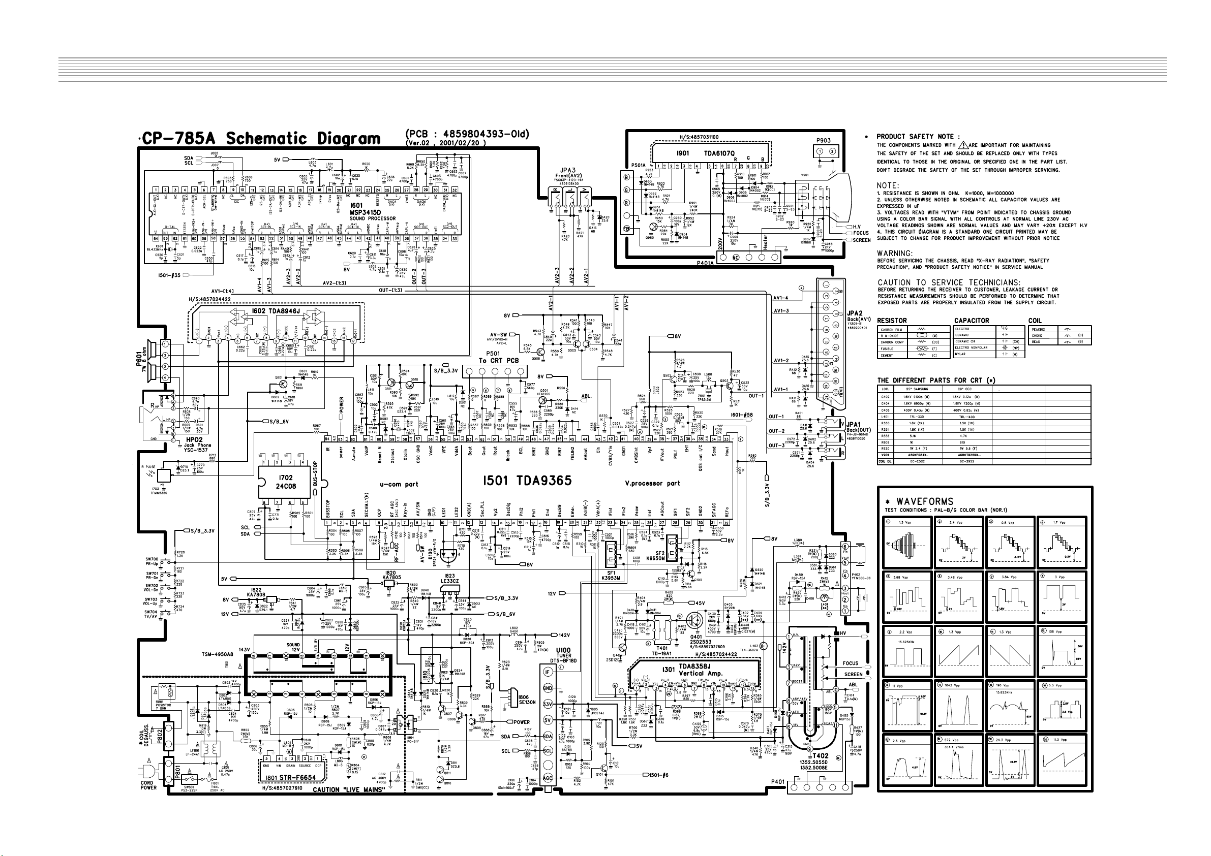
Service Manual CP-785A
-88-
10. Circuit Diagram
10-1 Old Main PCB

Service Manual CP-785A
-89-
10. Circuit Diagram
10-2 New Main PCB & Control PCB

NEC Corporation
7-1, SHIBA 5-CHOME MINATO-KU,
TOKYO 108-8001, JAPAN
 Loading...