NEC 2SK3902 Technical data

DATA SHEET
MOS FIELD EFFECT TRANSISTOR
2SK3902
SWITCHING
N-CHANNEL POWER MOS FET
DESCRIPTION
The 2SK3902 is N-channel MOS Field Effect Transistor
designed for high current switching applications.
ORDERING INFORMATION
PART NUMBER PACKAGE
2SK3902-ZK
FEATURES
• Super low On-state resistance
DS(on)1 = 21 mΩ MAX. (VGS = 10 V, ID = 15 A)
R
R
DS(on)2 = 26 mΩ MAX. (VGS = 4.5 V, ID = 15 A)
• Low C
iss: C iss = 1200 pF TYP.
• Built-in gate protection diode
ABSOLUTE MAXIMUM RATINGS (TA = 25°C)
Drain to Source Voltage (VGS = 0 V) VDSS 60 V
Gate to Source Voltage (V
Drain Current (DC) (T
Drain Current (pulse)
Total Power Dissipation (T
Total Power Dissipation (T
Channel Temperature T
Storage Temperature T
Single Avalanche Energy
Repetitive Avalanche Current
Repetitive Avalanche Energy
Notes 1. PW ≤ 10
2. Starting T
3. R
G = 25 Ω, Tch(peak) ≤ 150°C
DS = 0 V) VGSS ±20 V
C = 25°C) ID(DC) ±30 A
Note1
C = 25°C) PT1 45 W
A = 25°C) PT2 1.5 W
Note2
Note3
Note3
µ
s, Duty Cycle ≤ 1%
ch = 25°C, VDD = 30 V, RG = 25 Ω, VGS = 20 → 0 V, L = 100
I
D(pulse) ±90 A
ch 150 °C
stg −55 to +150 °C
E
AS 40 mJ
AR 20 A
I
E
AR 40 mJ
µ
H
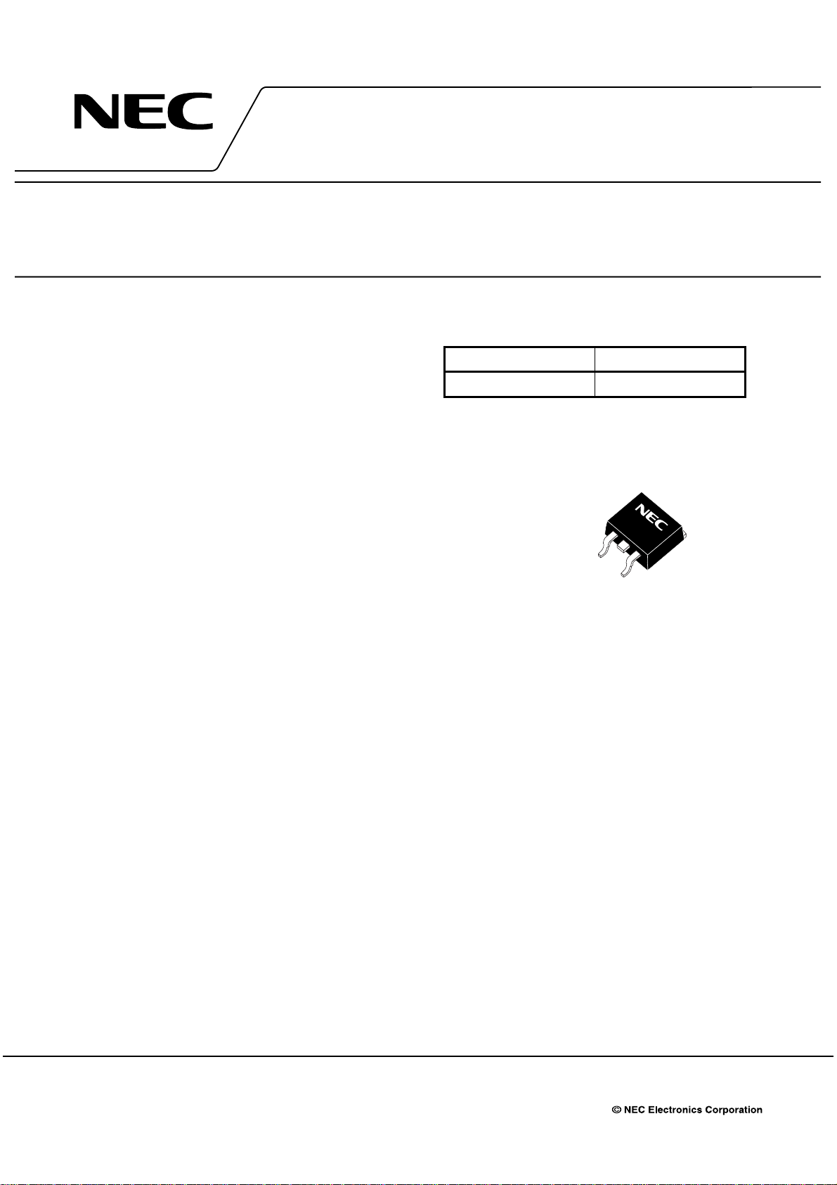
TO-263 (MP-25ZK)
(TO-263)
The information in this document is subject to change without notice. Before using this document, please
confirm that this is the latest version.
Not all products and/or types are available in every country. Please check with an NEC Electronics
sales representative for availability and additional information.
Document No. D17177EJ1V0DS00 (1st edition)
Date Published May 2004 NS CP(K)
Printed in Japan
2004

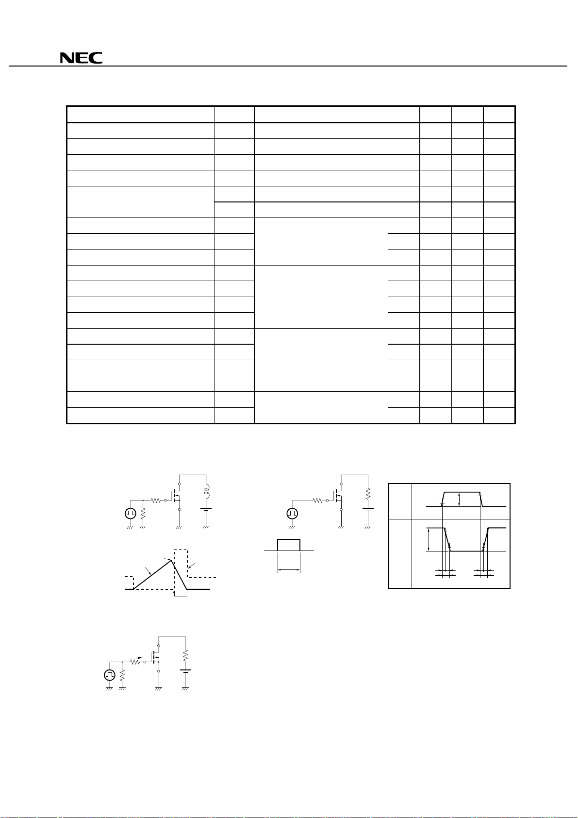
ELECTRICAL CHARACTERISTICS (TA = 25°C)
CHARACTERISTICS SYMBOL TEST CONDITIONS MIN. TYP. MAX. UNIT
2SK3902
Zero Gate Voltage Drain Current IDSS VDS = 60 V, VGS = 0 V 10
Gate Leakage Current IGSS VGS = ±20 V, VDS = 0 V ±10
µ
A
µ
A
Gate Cut-off Voltage VGS(off) VDS = 10 V, ID = 1 mA 1.5 2.0 2.5 V
Note
Forward Transfer Admittance
Drain to Source On-state Resistance
Note
fs | VDS = 10 V, ID = 15 A 9.5 19 S
| y
DS(on)1 VGS = 10 V, ID = 15 A 16.8 21 mΩ
R
RDS(on)2 VGS = 4.5 V, ID = 15 A 19.5 26 mΩ
Input Capacitance Ciss VDS = 10 V 1200 pF
Output Capacitance Coss VGS = 0 V 250 pF
Reverse Transfer Capacitance Crss f = 1 MHz 85 pF
Turn-on Delay Time td(on) VDD = 30 V, ID = 15 A 10 ns
Rise Time tr VGS = 10 V 4 ns
Turn-off Delay Time td(off) RG = 0 Ω 37 ns
Fall Time tf 4 ns
Total Gate Charge QG VDD = 48 V 25 nC
Gate to Source Charge QGS VGS = 10 V 4.5 nC
Gate to Drain Charge QGD ID = 30 A 6.0 nC
Note
Body Diode Forward Voltage
F(S-D) IF = 30 A, VGS = 0 V 0.92 1.5 V
V
Reverse Recovery Time trr IF = 30 A, VGS = 0 V 31 ns
Reverse Recovery Charge Qrr di/dt = 100 A/µs 34 nC
Note Pulsed
TEST CIRCUIT 1 AVALANCHE CAPABILITY
TEST CIRCUIT 2 SWITCHING TIME
D.U.T.
G
= 25 Ω
R
PG.
50 Ω
VGS = 20 → 0 V
BV
DSS
I
AS
I
D
V
DD
TEST CIRCUIT 3 GATE CHARGE
D.U.T.
G
= 2 mA
I
PG.
50 Ω
2
V
DS
Starting T
L
R
V
DD
L
V
DD
PG.
V
GS
D.U.T.
R
G
L
R
V
DD
0
τ
µ
τ = 1 s
ch
Duty Cycle ≤ 1%
V
GS
Wave Form
V
DS
Wave Form
V
GS
10%
0
V
DS
90%
V
DS
0
10% 10%
t
d(on)trtd(off)tf
t
on
90%
V
GS
90%
t
off
Data Sheet D17177EJ1V0DS

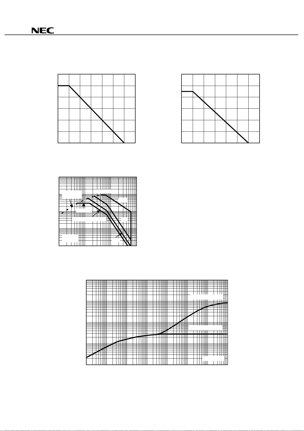
TYPICAL CHARACTERISTICS (TA = 25°C)
DERATING FACTOR OF FORWARD BIAS
SAFE OPERATING AREA
120
TOTAL POWER DISSIPATION vs.
CASE TEMPERATURE
60
2SK3902
dT - Percentage of Rated Power - %
100
80
60
40
20
0
0 25 50 75 100 125 150 175
T
C - Case Temperature - °C
50
40
30
20
10
0
PT - Total Power Dissipation - W
0 25 50 75 100 125 150 175
T
C - Case Temperature - °C
FORWARD BIAS SAFE OPERATING AREA
1000
I
= 90 A
100
10
R
Limited
DS(on)
= 10 V)
(at V
GS
I
D(DC)
Power Dissipation Limited
D(pulse)
100 µs
= 30 A
1 ms
1
TC = 25°C
ID - Drain Current - A
Single pulse
10 ms
0.1
0.1 1 10 100
V
DS - Drain to Source Voltage - V
TRANSIENT THERMAL RESISTANCE vs. PULSE WIDTH
1000
100
10
1
0.1
rth(t) - Transient Thermal Resistance - °C/W
µ
1 m 10 m 100 m 1 10 100 1000
100
PW - Pulse Width - s
Data Sheet D17177EJ1V0DS
R
R
th(ch-C)
th(ch-A)
= 83.3°C/W
= 2.78°C/W
Single pulse
3
 Loading...