

NEC 2SK3432-Z Datasheet
PRELIMINARY DATA SHEET
MOS FIELD EFFECT TRANSISTOR
SWITCHING
N-CHANNEL POWER MOS FET
INDUSTRIAL USE
2SK3432
DESCRIPTION
The 2SK3432 is N-channel MOS Field Effect Transistor
designed for high current switching applications.
FEATURES
•Super low on-state resistance:
★
DS(on)1
= 4.0 mΩ MAX. (VGS = 10 V, ID = 42 A)
R
★
DS(on)2
= 6.9 mΩ MAX. (VGS = 4 V, ID = 42 A)
R
iss
iss
: C
•Low C
= 9500 pF TYP.
•Built-in gate protection diode
ABSOLUTE MAXIMUM RATINGS (TA = 25°C)
GSS
D(DC)
D(pulse)
I
AS
I
E
DSS
T
T
ch
stg
AS
Drain to Source Voltage V
Gate to Source Voltage V
Drain Current (DC) I
Drain Current (pulse)
Total Power Dissipation (T
Total Power Dissipation (T
Channel Temperature T
Storage Temperature T
★
Single Avalanche Current
★
Single Avalanche Energy
Notes 1.
PW ≤ 10
2.
Starting Tch = 25 °C, RG = 25 Ω, VGS = 20 V → 0 V
Note1
C
= 25°C) P
A
= 25°C) P
Note2
Note2
µ
s, Duty cycle ≤ 1 %
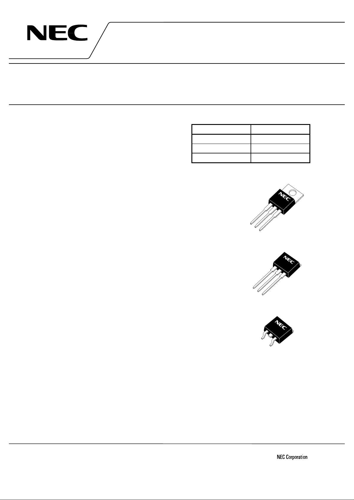
ORDERING INFORMATION
PART NUMBER PACKAGE
40 V
20 V
±
83 A
±
332 A
±
100 W
1.5 W
150 °C
–55 to +150 °C
69 A
476 mJ
2SK3432
2SK3432-S
2SK3432-Z
TO-220AB
TO-262
TO-220SMD
(TO-220AB)
(TO-262)
(TO-220SMD)
THERMAL RESISTANCE
Channel to Case Rth(ch-C) 1.25
Channel to Ambient Rth(ch-A) 83.3
The information in this document is subject to change without notice. Before using this document, please
confirm that this is the latest version.
Not all devices/types available in every country. Please check with local NEC representative for
availability and additional information.
Document No. D14601EJ1V0DS00 (1st edition)
Date Published March 2000 NS CP(K)
Printed in Japan
The mark ★ shows major revised points.
C/W
°
C/W
°
©
1999, 2000
ELECTRICAL CHARACTERISTICS (TA = 25 °C)
CHARACTERISTICS SYMBOL TEST CONDITIONS MIN. TYP. MAX. UNIT
★
Drain to Source On-state Resi stance R
★
Gate to Source Cut-off Voltage V
★
Forward Transfer Admittance | yfs |VDS = 10 V, ID = 42 A 40 80 S
Drain Leakage Current I
Gate to Source Leakage Current I
Input Capacitance C
Output Capacitance C
Reverse Transfer Capacitance C
★
Turn-on Delay Time t
★
Rise Time t
★
Turn-off Delay Time t
★
Fall Time t
★
Total Gate Charge Q
★
Gate to Source Charge Q
★
Gate to Drain Charge Q
Body Diode Forward Voltage V
★
Reverse Recovery Time t
★
Reverse Recovery Charge Q
DS(on)1VGS
DS(on)2VGS
R
GS(off)VDS
DSS
GSS
iss
oss
rss
d(on)ID
r
d(off)
f
G
GS
GD
F(S-D)IF
rr
rr
= 10 V, ID = 42 A 3.2 4.0 m
= 4 V, ID = 42 A 4.8 6.9 m
= 10 V, ID = 1 mA 1.5 2.0 2.5 V
VDS = 40 V, VGS = 0 V 10
VGS = ±20 V, VDS = 0 V
VDS = 10 V, VGS = 0 V, f = 1 MHz 9500 pF
2200 pF
920 pF
= 42 A, V
RG = 10
GS(on)
= 10 V, VDD = 20 V, 140 ns
Ω
1800 ns
470 ns
410 ns
ID = 83 A , VDD = 32 V, VGS = 10 V 150 nC
29 nC
45 nC
= 83 A, VGS = 0 V1.0V
IF = 83 A, VGS = 0 V, 69 ns
di/dt = 100 A/µ s 130 nC
2SK3432
µ
10
±
µ
Ω
Ω
A
A
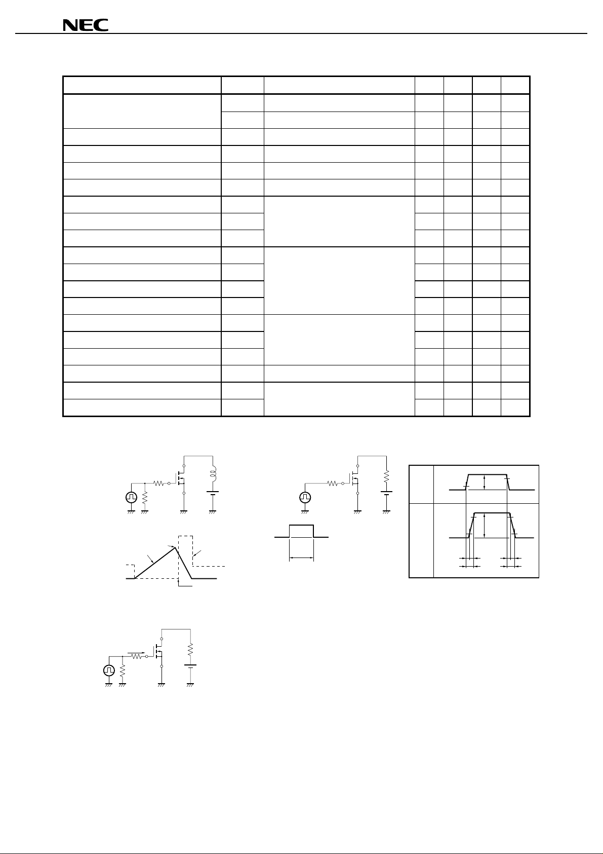
TEST CIRCUIT 1 AVALANCHE CAPABILITY
PG.
VGS = 20 → 0 V
V
G
R
DD
= 25 Ω
50 Ω
I
D
D.U.T.
I
AS
BV
DSS
V
DS
Starting T
L
DD
V
ch
TEST CIRCUIT 3 GATE CHARGE
D.U.T.
I
G
PG.
= 2 mA
50 Ω
R
L
V
DD
TEST CIRCUIT 2 SWITCHING TIME
D.U.T.
R
PG.
V
GS
0
τ
τ = 1 µs
Duty Cycle ≤ 1 %
G
V
V
GS
Wave Form
I
D
Wave Form
GS
10 %
0
I
D
10 %10
0
t
d(on)
V
90
%
I
trt
t
on
GS(on)
D
d(off)tf
%
90
90
%
%
t
off
L
R
V
DD
2
Preliminary Data Sheet D14601EJ1V0DS00
 Loading...