

NEC 2SK2159 Datasheet
DATA SHEET
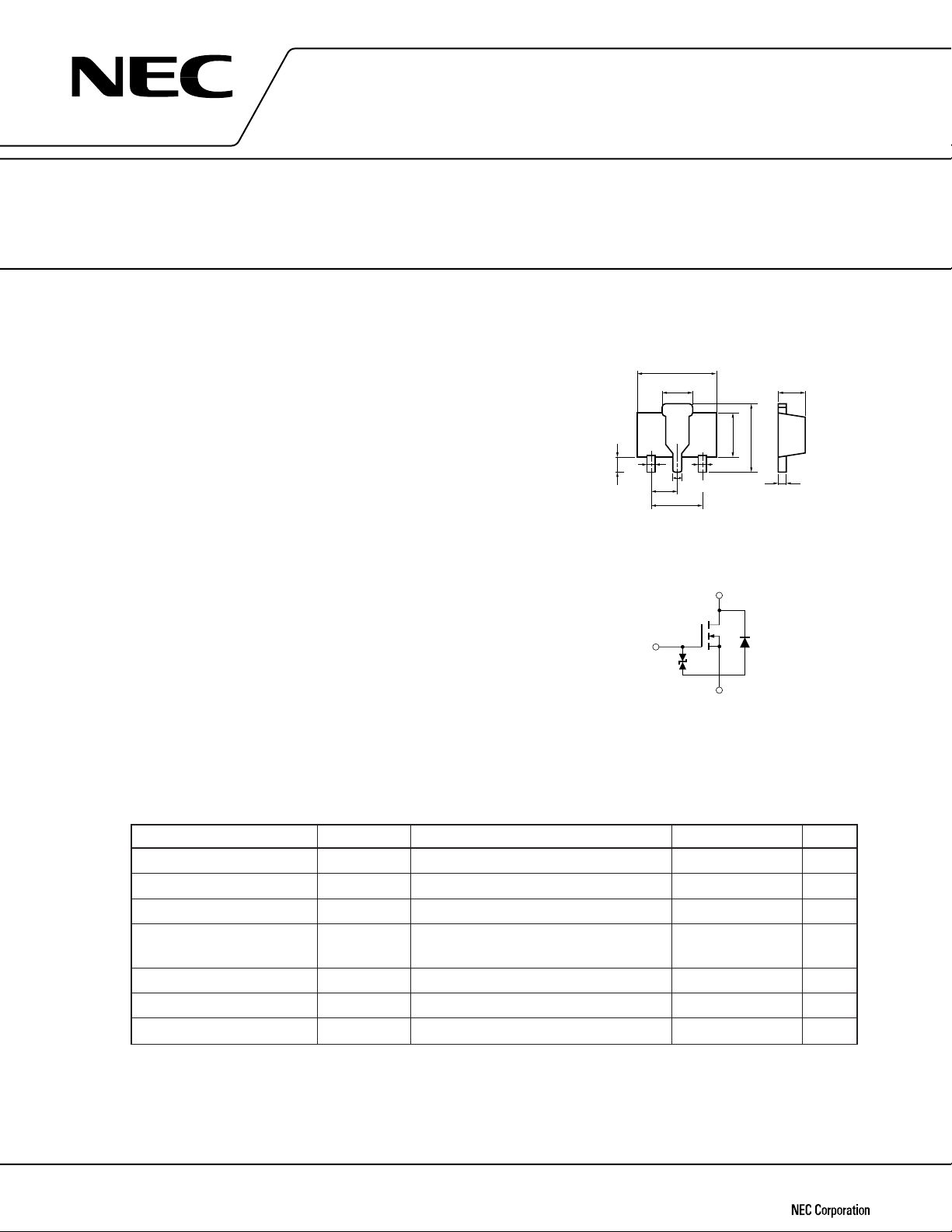
4.5 ± 0.1
1.6 ± 0.2
1
2
3
2.5 ± 0.1
4.0 ± 0.25
3.0
1.5
0.42 ± 0.06
0.47
± 0.06
0.8 MIN.
0.42
± 0.06
1.5 ± 0.1
0.41
–0.05
+0.03
2
3
Gate protection
diode
Internal diode
1
PACKAGE DIMENSIONS
(in millimeters)
EQUIVALENT CIRCUIT
PIN CONNECTION
1. Source (S)
2. Drain (D)
3. Gate (G)
Marking: NW
MOS FIELD EFFECT TRANSISTOR
N-CHANNEL MOS FET
FOR HIGH-SPEED SWITCHING
The 2SK2159 is an N-channel vertical type MOS FET featuring an operating voltage as low as 1.5 V. Because it can be
driven on a low voltage and it is not necessary to consider
driving current, the 2SK2159 is suitable for driving actuators of
low-voltage portable systems such as headphone stereo sets
and camcorders.
FEATURES
• Capable of drive gate with 1.5 V
• Small R
RDS(on) = 0.7 Ω MAX. @VGS = 1.5 V, ID = 0.1 A
RDS(on) = 0.3 Ω MAX. @VGS = 4.0 V, ID = 1.0 A
DS(on)
2SK2159
Document No. D11235EJ2V0DS00 (2nd edition)
Date Published June 1996 P
Printed in Japan
ABSOLUTE MAXIMUM RATINGS (TA = 25 ˚C)
Drain to Source Voltage VDSS VGS = 0 60 V
Gate to Source Voltage VGSS VDS = 0 ±14 V
Drain Current (DC) ID(DC) ±2.0 A
Drain Current (pulse) ID(pulse) PW ≤ 10 ms, ±4.0 A
Total Power Dissipation PT
Channel Temperature Tch 150 ˚C
Storage Temperature Tstg –55 to +150 ˚C
PARAMETER SYMBOL TEST CONDITIONS RATINGS UNIT
Duty Cycle ≤ 50 %
Mounted on 16 cm2 × 0.7 mm ceramic substrate.
2.0 W
©
1996
ELECTRICAL CHARACTERISTICS (TA = 25 ˚C)
PARAMETER SYMBOL TEST CONDITIONS MIN. TYP. MAX. UNIT
Drain Cut-off Current IDSS VDS = 60 V, VGS = 0 1.0
Gate Leakage Current IGSS VGS = ±14 V, VDS = 0 ±10
Gate Cut-off Voltage V GS(off) VDS = 10 V, ID = 1 mA 0.5 0.9 1.1 V
Forward Transfer Admittance | yfs |VDS = 10 V, ID = 1.0 A 0.4 S
Drain to Source On-state Resistance
Drain to Source On-state Resistance
Drain to Source On-state Resistance
Input Capacitance Ciss VDS = 10 V, VGS = 0, 319 pF
Output Capacitance Coss
Reverse Transfer Capacitance Crss 22 pF
Turn-On Delay Time td(on) VDD = 25 V, ID = 1.0 A 38 ns
Rise Time tr
Turn-Off Delay Time td(off)
Fall Time tf 130 ns
RDS(on)1 VGS = 1.5 V, ID = 0.1 A 0.55 0.7 Ω
RDS(on)2 VGS = 2.5 V, ID = 1.0 A 0.27 0.5 Ω
RDS(on)3 VGS = 4.0 V, ID = 1.0 A 0.22 0.3 Ω
f = 1.0 MHz
VGS(on) = 3 V, RG = 10 Ω
RL = 25 Ω
109 pF
128 ns
237 ns
2SK2159
µ
A
µ
A
2
 Loading...