NEC 2SC2570A-T, 2SC2570A Datasheet

DATA SHEET
NPN SILICON TRANSISTOR
2SC2570A
HIGH FREQUENCY LOW NOISE AMPLIFIER
NPN SILICON EPITAXIAL TRANSISTOR
DESCRIPTION
The 2SC2570A is designed for use in Low Noise Amplifier of VHF & UHF stages.
FEATURES
• Low noise and high gain : NF = 1.5 dB TYP., Ga = 8 dB TYP. @f = 1.0 GHz, VCE = 10 V, IC = 5.0 mA
• Wide dynamic range : NF = 1.9 dB, Ga = 9 dB @f = 1 GHz, VCE = 10 V, IC = 15 mA
ORDERING INFORMATION
Part Number Quantity
2SC2570A Loose products (500 pcs)
2SC2570A-T Taping products (Box type) (2 500 pcs)
Remark
To order evaluation samples, please contact your NEC sales office (available in 500-pcs units).
ABSOLUTE MAXIMUM RATINGS (TA = +25 °C)
Parameter Symbol Ratings Unit
Collector to Base Voltage V
Collector to Emitter Voltage V
Emitter to Base Voltage V
Collector Current I
Total Power Dissipat i on P
Junction Temperature T
Storage Temperature T
CBO
CEO
EBO
C
tot
j
stg
25 V
12 V
3.0 V
70 mA
600 mW
150 °C
–65 to +150 °C
The information in this document is subject to change without notice. Before using this document, please
confirm that this is the latest version.
Not all devices/types available in every country. Please check with local NEC representative for
availability and additional information.
Document No. P10404EJ3V0DS00 (3rd edition)
Date Published November 1999 N CP(K)
Printed in Japan
©
1980, 1999

2SC2570A
ELECTRICAL CHARACTERISTICS (TA = +25 °C)
Parameter Symbol Test Conditions MIN. TYP. MAX. Unit
Note 1
FE
DC Current Gain
Gain Bandwidth Product f
Output Capacitance
Insertion Power Gain
Noise Figure NF VCE = 10 V, IC = 5 mA, f = 1.0 GHz – 1.5 3.0 dB
Maximum Available Gain MAG VCE = 10 V, IC = 20 mA, f = 1.0 GHz – 11.5 – dB
Collector Cutoff Current I
Emitter Cutoff Current I
h
Ob
C
|
S
CBO
EBO
VCE = 10 V, IC = 20 mA 40 – 200 –
T
VCE = 10 V, IC = 20 mA – 5.0 – GHz
Note 2
VCB = 10 V, IE = 0, f = 1.0 MHz – 0.7 0.9 pF
2
|
21e
VCE = 10 V, IC = 20 mA, f = 1.0 GHz 8 10 – dB
VCB = 15 V, IE = 0 – – 0.1
VEB = 2.0 V, IC = 0 – – 0.1
µ
A
µ
A
Notes 1.
Pulse Measurement: PW ≤ 350
The emitter and case terminal should be connected to the guard terminal of the capacitance bridge.
2.
s, Duty Cycle ≤ 2%
µ
2
Data Sheet P10404EJ3V0DS00

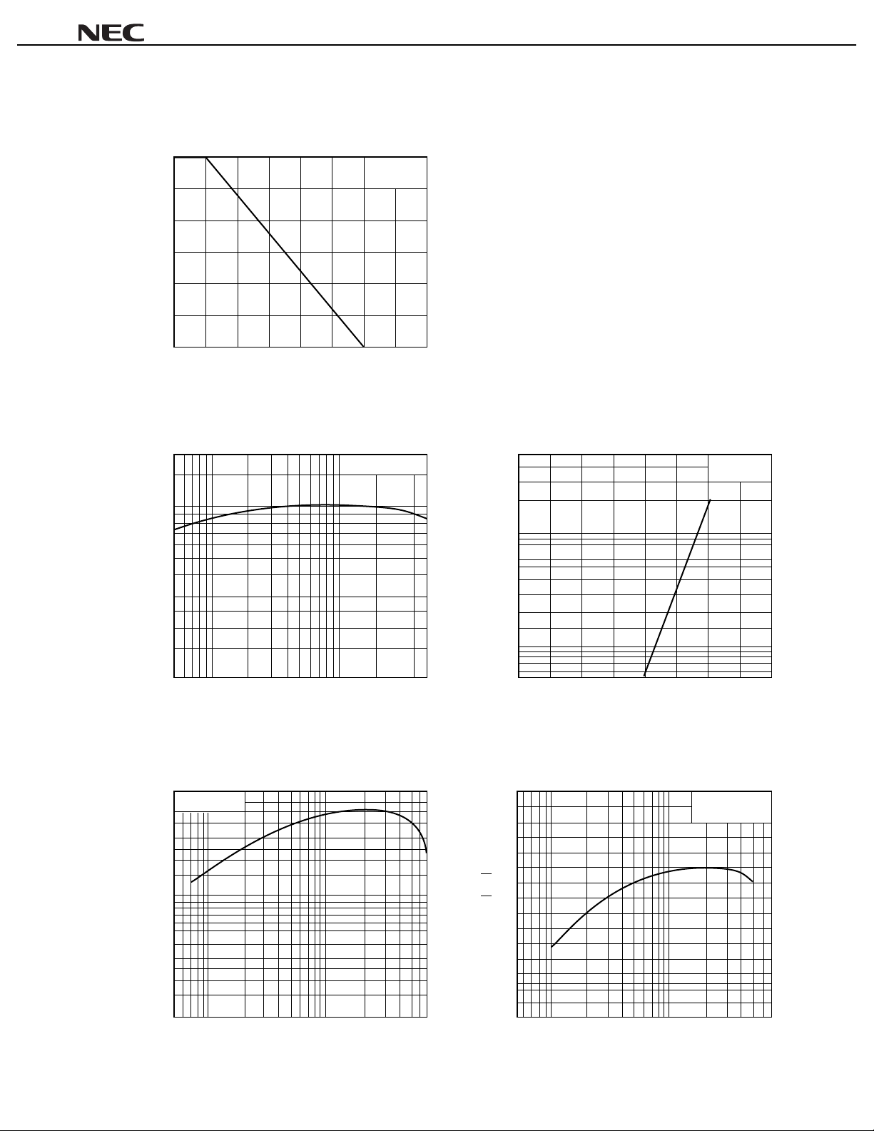
TYPICAL CHARACTERISTICS (TA = +25 °C)
TOTAL POWER DISSIPATION vs.
AMBIENT TEMPERATURE
600
free Air
(mW)
T
400
200
Total Power Dissipation P
0 50 100
Operating Ambient Temperature T
150 200
A
(°C)
2SC2570A
DC CURRENT GAIN vs.
COLLECTOR CURRENT
200
100
FE
50
DC Current Gain h
20
10
0.5 1 5
Collector Current I
GAIN BANDWIDTH PRODUCT vs.
COLLECTOR CURRENT
7
VCE = 10 V
5
)
Z
VCE = 10 V
10 50
C
(mA)
COLLECTOR CURRENT vs.
BASE TO EMITTER VOLTAGE
50
(mA)
10
C
5
Collector Current I
1
0.5
0.5 0.6 0.7
Base to Emitter Voltage V
INSERTION GAIN vs.
COLLECTOR CURRENT
15
VCE = 10 V
0.8
BE
(V)
VCE = 10 V
f = 1.0 GH
0.9
Z
(GH
T
2
1
0.5
0.2
Gain Bandwidth Product f
0.1
0.5 1 5
Collector Current I
10 7050
C
(mA)
Data Sheet P10404EJ3V0DS00
(dB)
10
2
21e
5
Insertion Gain S
0
0.5 1 5
10
Collector Current I
C
(mA)
7050
3
 Loading...