NEC 2SC2148 Datasheet

DATA SHEET
2SC2148, 2SC2149
MICROWAVE LOW NOISE AMPLIFIER
NPN SILICON EPITAXIAL TRANSISTOR
DESCRIPTION
The 2SC2148, 2SC2149 are economical microwave transistors
encapsulated into new hermetic stripline packages, "micro X".
These are designed for small signal amplifier, low noise amplifier,
and oscillator applications in the L to C band, and CML circuit use.
SILICON TRANSISTORS
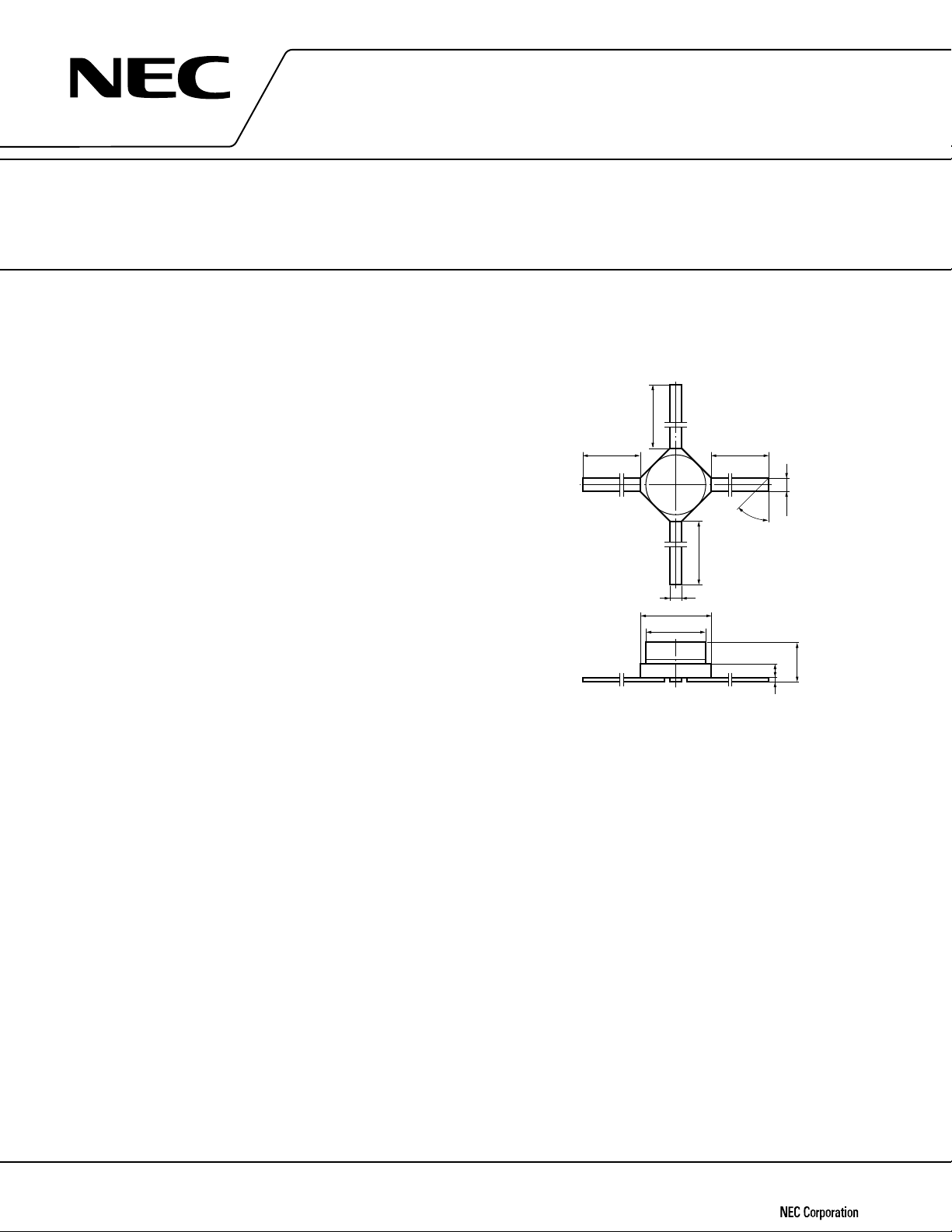
PACKAGE DIMENSIONS
(Unit : mm)
1
FEATURES
2SC2148 NF: 2.1 dB TYP. @f = 500 MHz
2SC2149 NF: 2.6 dB TYP. @f = 2.0 GHz
4.0 MIN.
2
4.0 MIN.
1.
2.
3.
4.
3
2.55±0.2
2.1
φ
Emitter
Collector
Emitter
Base
4.0 MIN.
4.0 MIN.
0.5±0.05
45°
4
0.55
+0.06
−0.03
0.1
0.5±0.05
1.8 MAX.
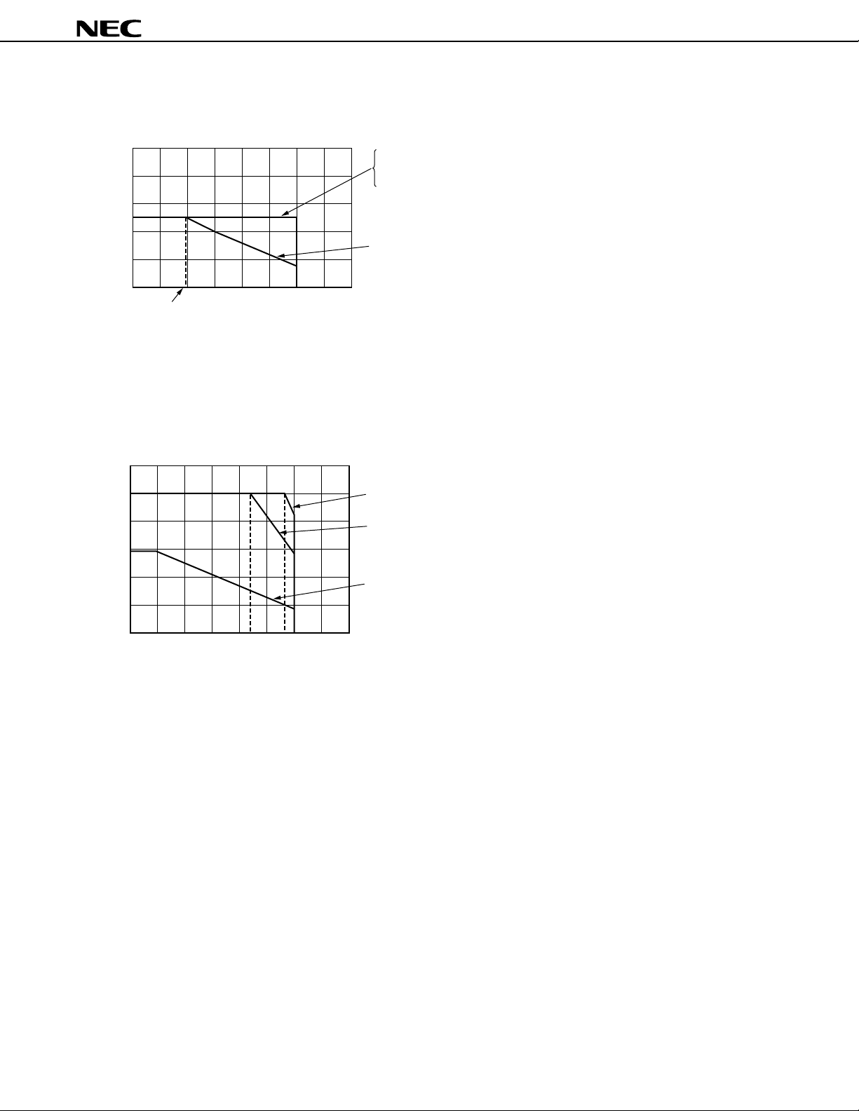
Derating curves of the 2SC2148, 2SC2149.
The maximum junction temperature of these transistors is allowed up to 200 °C, but the ambient or storage
temperature is limitted to 150 °C. The operating junction temperature is estimated with power consumption (PT) and
thermal resistance mentioned on these derating curves.
The information in this document is subject to change without notice.
Document No. P11809EJ2V0DS00 (2nd edition)
(Previous No. TC-1428)
Date Published August 1996 P
Printed in Japan
©
1981

2SC2148
500
400
300
TOTAL POWER DISSIPATION vs.
AMBIENT TEMPERATURE
th(j-c)
with infinite heat sink; R
130 °C/W
mounting on ceramic boad with solder
(Al
2O3
20 × 50 × 0.635 mm)
; R
th(j-a)
190 °C/W
2SC2148, 2SC2149
200
100
−Total Power Dissipation−mW
T
0
P
2SC2149
600
400
200
−Total Power Dissipation−mW
T
P
0
50
100
150 200
48
TA−Ambient Temperature−°C
TOTAL POWER DISSIPATION vs.
AMBIENT TEMPERATURE
50 100 110 140150 200
TA−Ambient Temperature−°C
free-air; R
with infinite heat sink; R
th(j-a)
610 °C/W
th(j-c)
120 °C/W
mounting on ceramic boad with solder
(Al
2O3
20 × 50 × 0.635 mm)
th(j-a)
180 °C/W
; R
free-air; R
th(j-a)
600 °C/W
2

2SC2148, 2SC2149
2SC2148
ABSOLUTE MAXIMUM RATINGS (TA = 25 °C)
Collector to Base Voltage VCBO 30 V
Collector to Emitter Voltage VCEO 14 V
Emitter to Base Voltage VEBO 3.0 V
Collector Current I
Total Power Dissipation PT(TA = 48 °C) 250 mW
Total Power Dissipation PT(Tc = 150 °C) 250 mW
Junction Temperature T
Storage Temperature Tstg −65 to +150 °C
ELECTRICAL CHARACTERISTICS (TA = 25 °C)
CHARACTERISTIC SYMBOL MIN. TYP. MAX. UNIT TEST CONDITIONS
Collector Cutoff Current ICBO 0.1
Emitter Cutoff Current IEBO 0.1
DC Current Gain hFE 30 80 200 VCE = 10 V, IC = 10 mA
Gain Bandwidth Product fT 3.0 GHz VCE = 10 V, IC = 10 mA
Output Capacitance * Cob 0.55 pF VCB = 10 V, IE = 0, f = 1.0 MHz
Insertion Gain S21e
Noise Figure NF 2.1 3.5 dB VCE = 10 V, IC = 3.0 mA, f = 500 MHz
Maximum Available Gain MAG 13.3 dB VCE = 10 V, IC = 10 mA, f = 1.0 GHz
C 50 mA
j 200 °C
2
7.5 9.3 dB VCE = 10 V, IC = 10 mA, f = 1.0 GHz
µ
AVCB = 15 V, IE = 0
µ
AVEB = 2.0 V, IC = 0
* The emitter terminal should be connected to the guard terminal of the three-terminal capacitance bridge.
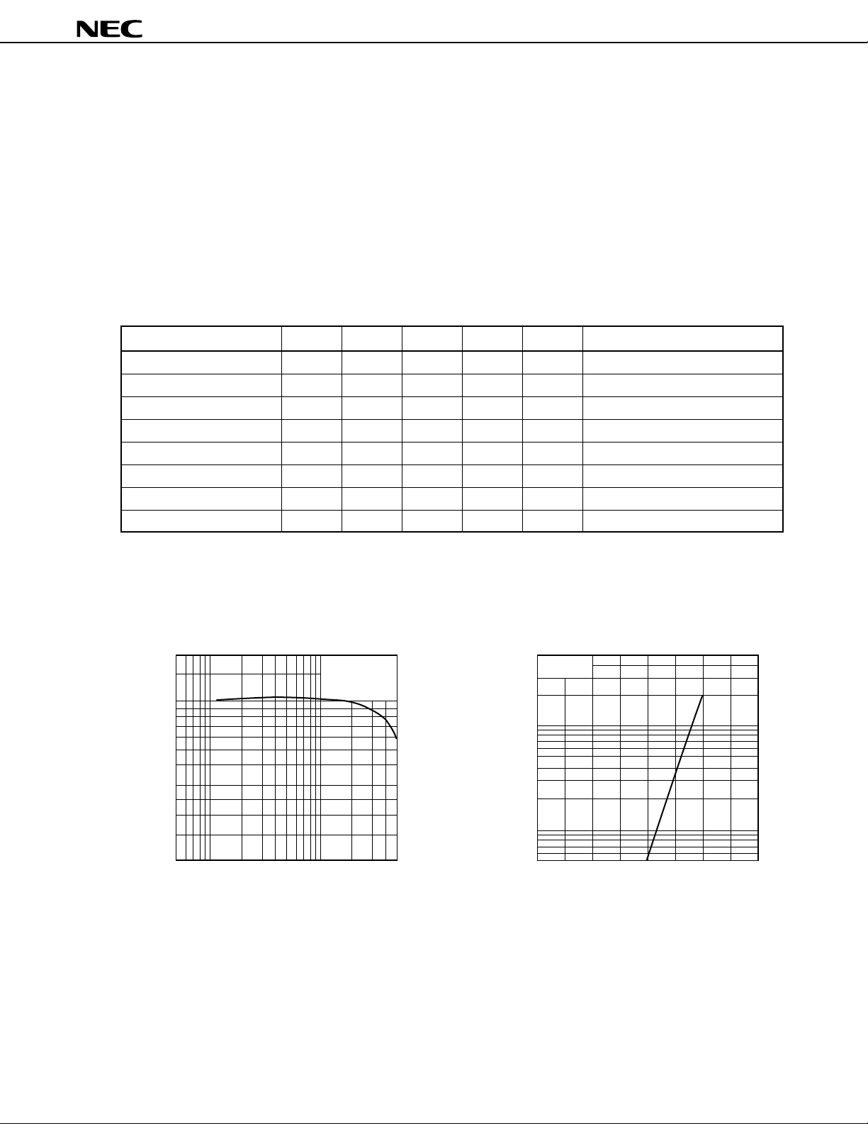
TYPICAL CHARACTERISTICS (TA = 25 °C)
DC CURRENT GAIN vs.
200
100
50
−DC Current Gain
FE
h
20
10
0.5 1 5
COLLECTOR CURRENT
C
−Collector Current−mA
I
CE
= 10 V
V
10 50
−Collector Current−mA
C
I
50
10
5
1
0.5
COLLECTOR CURRENT vs.
BASE TO EMITTER VOLTAGE
V
CE
= 10 V
0.5 0.6 0.7 0.8 0.9
VBE−Base to Emitter Voltage−V
3
 Loading...