NEC 2SA1988 Datasheet

PNP SILICON TRANSISTOR
MP-88
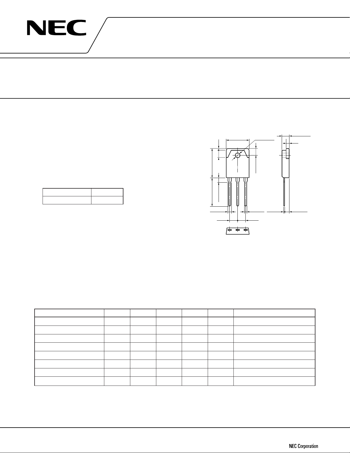
1.Base
2.Collector
3.Emitter
4.Fin (Collector)
1 2 3
15.7 MAX. 3.2±0.2
4.5±0.2
5.0 1.03.4MAX.
20.5MAX.19 MIN.
2.2±0.2
5.45 5.45
1.0±0.2
4
4.7 MAX.
1.5
2.8±0.10.6±0.1
φ
POWER AMPLIFIER
INDUSTRIAL USE
DESCRIPTION
The 2SA1988 is PNP Silicon Power Transistor that
designed for audio frequency power amplifier.
FEATURES
• High Voltage VCEO = −200 V
• DC Current Gain h
• TO-3P Package
FE = 70 to 200
DATA SHEET
Silicon Power Transistor
2SA1988
PACKAGE DIMENSIONS
ORDERING INFORMATION
Type Number Package
2SA1988 MP-88
ABSOLUTE MAXIMUM RATINGS (TA = 25 °C)
Collector to Base Voltage VCBO −200 V
Collector to Emitter Voltage V
Emitter to Base Voltage V
Collector Current (DC) I
Collector Current (pulse) I
Total Power Dissipantion P
JunctionTemperature T
Storage Tempreature T
*1 PW ≤ 300
µ
s, Duty Cycle ≤ 10 % *2 TC = 25 °C
CEO −200 V
EBO −5.0 V
C (DC) −7.0 A
C (pulse) *1 -10 A
2 *2 100 W
J 150 °C
stg −55 to +150 °C
ELECTRICAL CHARACTERISTICS (TA = 25 °C)
CHARACTERISTIC SYMBOL MIN. TYP. MAX. UNIT TEST CONDITIONS
Collector Cutoff Current ICBO −50
Emitter Cutoff Current IEBO −50
DC Current Gain hFE1 70 200 − VCE = −5.0 V, IC = −1.0 A ∗
DC Current Gain hFE2 20 − VCE = −5.0 V, IC = −3.5 A ∗
Collector Saturation Voltage VCE (sat) −0.6 −2.0 V IC = −5.0 V, IE = −0.5 V ∗
Base Saturation Voltage VBE (sat) −1.3 −2.0 V IC = −5.0 V, IE = −0.5 V ∗
Gain Band width Product fT 40 MHz VCE = −5.0 V, IC = 1.0 mA
Output Capacitance Cob 270 pF VCB = −10 V, IC = 0, f = 1.0 MHz
∗ Pulse Test PW ≤ 350 µs, Duty Cycle ≤ 2 %
µ
AVCB = −200 V, IE = 0
µ
AVEB = −3.0 V, IC = 0
Document No. D11176EJ1V0DS00 (1st edition)
Date Published May 1996 P
Printed in Japan
The information in this document is subject to change without notice.
©
1996

CHARACTERISTICS (TA = 25 °C)
2SA1988
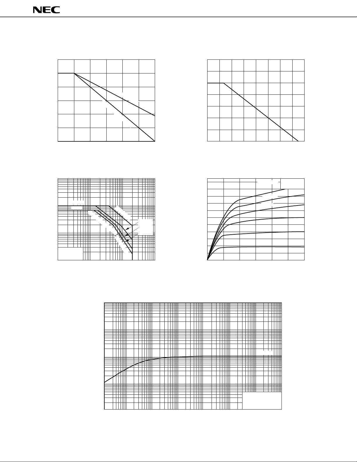
DERATING FACTOR OF FORWARD BIAS
SAFE OPERATING AREA
100
80
S/b Limited
60
Dissipation Limited
40
20
dT - Percentage of Rated Power - %
0
50 100 150
T
C - Case Temperature - °C
FORWARD BIAS SAFE OPERATING AREA
-100
-10
-1
IC(Pulse)
IC(DC)
Dissipation Limited
PW=1ms
S/b Limited
IC - Collector Current - A
TC = 25 °C
Single Pulse
-0.1
-1
V
-10 -100 -1000
CE - Collector to Emitter Voltage - V
10ms
100ms
200ms
TOTAL POWER DISSIPATION vs.
CASE TEMPERATURE
140
120
100
80
60
40
20
PT - Total Power Dissipation - W
0
20
40 60 80 100 120 140 160
T
C - Case Temperature - °C
COLLECTOR CURRENT vs.
COLLECTOR TO EMITTER VOLTAGE
-12
-10
-8
-6
-4
IC - Collector Current - A
-2
0
V
-10
CE - Collector to Emitter Voltage - V
IB=120mA
100mA
80mA
60mA
40mA
20mA
-20
Pulsed
-30
TRANSIENT THERMAL RESISTANCE vs. PULSE WIDTH
100
10
1
Rth (J-C)
0.1
rth(t) - Transient Thermal Resistance - °C/W
0.01
1 m 10 m 100 m 1 10 100 1 000 100
µ
Single Pulse
TC=25°C
PW - Pulse Width - s
2
 Loading...