

DATA SHEET
p
SILICON SWITCHING DI ODE
1SS303
HIGH SPEED SWITCHING
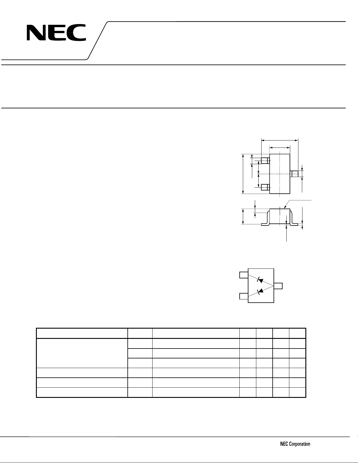
SILICON EPITAXIAL DOUBLE DIODE : COMMON ANODE
FEATURES
• Low capacitance: Ct
• High speed switching: t
• Wide applications including switching, limitter, clipper.
• Double diode configuration assures economical use.
= 2.5 pF TYP.
= 4.0 ns MAX.
rr
ABSOLUTE MAXIMUM RATINGS
Maximum Voltages and Currents (TA = 25°C)
Peak Reverse Voltage V
DC Reverse Voltage V
Note
Surge Current (1
Surge Current (1
Peak Forward Current
s)
µ
s) I
µ
Note
Peak Forward Current I
Average Rectified Current
Note
Average Rectified Current I
Maximum Temperatures
Junction Temperature T
Storage Temperature Range T
Thermal Resistance
Junction to Ambient
Note
Junction to Ambient R
Both diodes loaded simultaneously.
Note
R
I
FSM
FSM
I
FM
FM
I
th(j-a)
th(j-a)
RM
R
O
O
j
stg
75 V
50 V
6.0 A
4.0 A
450 mA
300 mA
150 mA
100 mA
150 °C
–55 to + 150 °C
1.0 °C/mW
0.85 °C/mW
PACKAGE DIMENSIONS (Unit: mm)
2.1±0.1
1.25±0.1
2
+0.1
−0
0.65
0.3
2.0±0.20.9±0.1
0.3
0.65
1
Marking
0 to 0.1
3
+0.1
−0
0.3
+0.1
−0.05
0.15
CONNECTION DIAGRAM (Top View)
2
3
1
Marking : A4
1. Cathode
2. Cathode
3. Anode
ELECTRICAL CHARACTERISTICS (TA = 25°C)
CHARACTERISTICS SYMBOL TEST CONDITIONS MIN. TYP. MAX. UNIT
Forward Voltage
Reverse Current I
Capacitance C
Reverse Recovery Time t
The information in this document is subject to change without notice. Before using this document, please
confirm that this is the latest version.
Not all devices/types available in every country. Please check with local NEC representative for
availability and additional information.
Document No. D16308EJ2V0DS00 (2nd edition)
(Previous No. DC-2100)
Date Published July 2002 NS CP(K)
Printed in Ja
an
F1
V
V
V
IF = 10 mA 0.72 1.0 V
F2
IF = 50 mA 0.88 1.1 V
F3
IF = 100 mA 1.0 1.2 V
R
VR = 50 V 0.1
t
VR = 0 V, f = 1.0 MHz 2.5 4.0 pF
rr
See Test Circuit. 4.0 ns
A
µ
©
1987
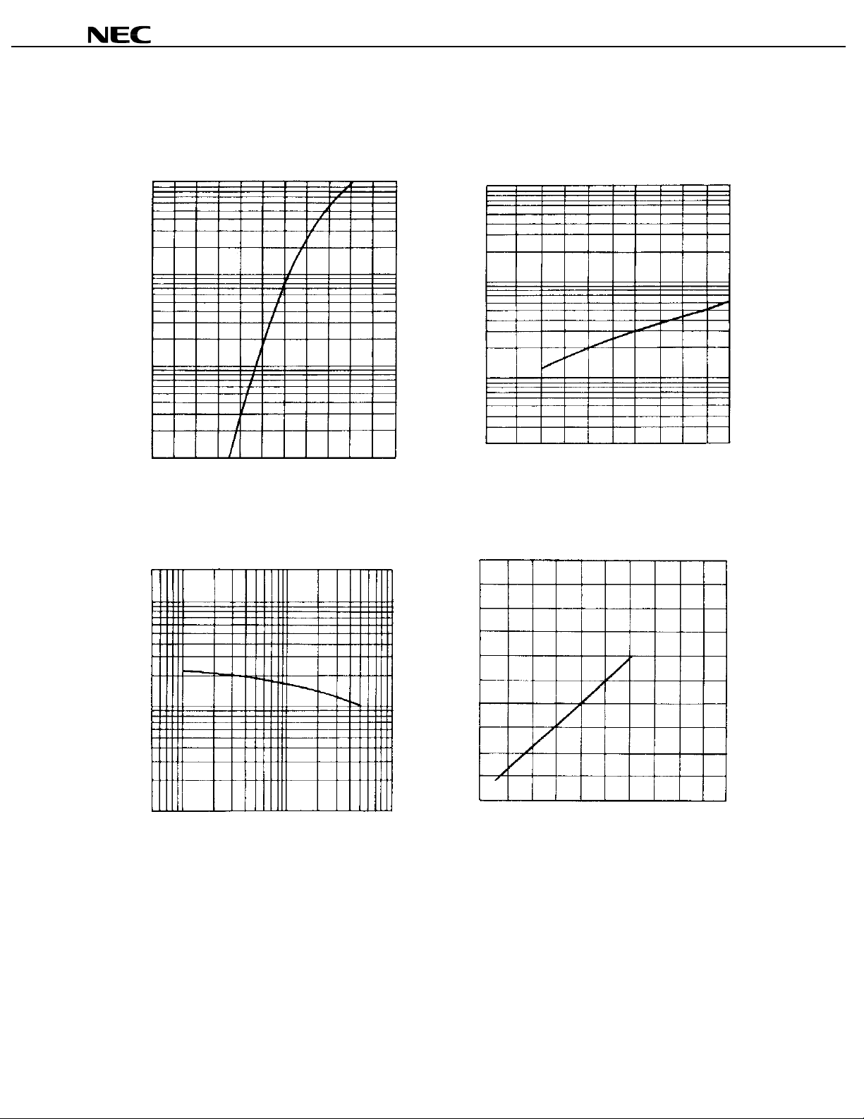
TYPICAL ELECTRICAL CURVES (TA = 25°C)
1SS303
100
50
20
10
5
2
1
- Forward Current - mA
F
I
0.5
0.2
0.1
0
0.2 0.4 0.6 0.8 1.0 1.2
20
FORWARD CURRENT vs.
FORWARD VOLTAGE
F
- Forward Voltage - V
V
TERMINAL CAPACITANCE vs.
REVERSE VOLTA GE
REVERSE CURRENT vs.
REVERSE VOLTA GE
100
50
20
10
5
2
- Reverse Current - µA
R
1
I
0.5
0.2
01020304050
R
- Reverse Voltage - V
V
REVERSE RECOVERY TIME vs.
FORWARD CURRENT
20
10
5
2
1
0.5
- Terminal Capacitance - pF
t
C
0.2
0.1
0.5 1 2 5 10 20 50 100
R
- Reverse Voltage - V
V
16
12
8
4
- Reverse Recovery Time - ns
rr
t
0 20 40 60 80 100
I
F
- Forward Current - mA
2
Data Sheet D16308EJ2V0DS

REVERSE RECOVERY TIME (trr) TEST CIRCUIT
1SS303
Pulse
Generator
(50 Ω)
DC
Source
0.02 µF D.U.T.
3 kΩ
+
−
F
= 10 mA, VR = 6.0 V, RL = 100 Ω
I
i
rr
= 0.1• I
Trigger
r
Sampling
Oscilloscope
(50 Ω)
Input Voltage
Waveform to Diode
V
F
0
V
R
Output Current
Waveform in Diode
I
F
0
I
r
0.1• I
r
rr
t
Data Sheet D16308EJ2V0DS
3

1SS303
•
The information in this document is current as of July, 2002. The information is subject to change
without notice. For actual design-in, refer to the latest publications of NEC's data sheets or data
books, etc., for the most up-to-date specifications of NEC semiconductor products. Not all products
and/or types are available in every country. Please check with an NEC sales representative for
availability and additional information.
•
No part of this document may be copied or reproduced in any form or by any means without prior
written consent of NEC. NEC assumes no responsibility for any errors that may appear in this document.
•
NEC does not assume any liability for infringement of patents, copyrights or other intellectual property rights of
third parties by or arising from the use of NEC semiconductor products listed in this document or any other
liability arising from the use of such products. No license, express, implied or otherwise, is granted under any
patents, copyrights or other intellectual property rights of NEC or others.
•
Descriptions of circuits, software and other related information in this document are provided for illustrative
purposes in semiconductor product operation and application examples. The incorporation of these
circuits, software and information in the design of customer's equipment shall be done under the full
responsibility of customer. NEC assumes no responsibility for any losses incurred by customers or third
parties arising from the use of these circuits, software and information.
•
While NEC endeavours to enhance the quality, reliability and safety of NEC semiconductor products, customers
agree and acknowledge that the possibility of defects thereof cannot be eliminated entirely. To minimize
risks of damage to property or injury (including death) to persons arising from defects in NEC
semiconductor products, customers must incorporate sufficient safety measures in their design, such as
redundancy, fire-containment, and anti-failure features.
•
NEC semiconductor products are classified into the following three quality grades:
"Standard", "Special" and "Specific". The "Specific" quality grade applies only to semiconductor products
developed based on a customer-designated "quality assurance program" for a specific application. The
recommended applications of a semiconductor product depend on its quality grade, as indicated below.
Customers must check the quality grade of each semiconductor product before using it in a particular
application.
"Standard": Computers, office equipment, communications equipment, test and measurement equipment, audio
and visual equipment, home electronic appliances, machine tools, personal electronic equipment
and industrial robots
"Special": Transportation equipment (automobiles, trains, ships, etc.), traffic control systems, anti-disaster
systems, anti-crime systems, safety equipment and medical equipment (not specifically designed
for life support)
"Specific": Aircraft, aerospace equipment, submersible repeaters, nuclear reactor control systems, life
support systems and medical equipment for life support, etc.
The quality grade of NEC semiconductor products is "Standard" unless otherwise expressly specified in NEC's
data sheets or data books, etc. If customers wish to use NEC semiconductor products in applications not
intended by NEC, they must contact an NEC sales representative in advance to determine NEC's willingness
to support a given application.
(Note)
(1) "NEC" as used in this statement means NEC Corporation and also includes its majority-owned subsidiaries.
(2) "NEC semiconductor products" means any semiconductor product developed or manufactured by or for
NEC (as defined above).
M8E 00. 4
 Loading...