

Page 1
N C
NCR DECISION MATE V
System Technical
Manual
- Hardware
Page 2
CP/M-80 and CP/M-86 are registered trademarks of Digital Re
search Inc.
MS-DOS is a trademark of Microsoft Inc.
Document Order Numbers
Augsburg Stock No.: 017-0032261B
MIRS Library, Dayton: ST-2104-35
Copyright ©1983 by NCR Corporation
Printed in the Federal Republic of Germany
Second Edition, July 1983
Dayton, Ohio
All Rights Reserved
It is the policy of NCR Corporation to improve products as new
technology, components, software, and firmware become available.
NCR Corporation, therefore, reserves the right to change speci
fications without prior notice.
All features, functions, and operations described herein may not
be marketed by NCR in all parts of the world. In some instances,
photographs are of equipment prototypes. Therefore, before using
this document, consult your dealer or NCR office for information
that is applicable and current.
Page 3
FOREWORD
The NCR DECISION MATE V System Technical Manuals are de
signed to provide both hardware and software information: they
are intended for designers, system integrators, programmers, and
other interested persons who require detailed information on the
construction and operation of the NCR DECISION MATE V.
Problems arising from any changes that you make to the
hardware or software of the NCR DECISION MATE V are your
responsibility. NCR cannot assist in resolving problems that may
arise when making changes to the hardware or software.
The first manual provides general information on the NCR
DECISION MATE V and its various options. Information is
included on how to identify the various models and kits that are
available. The hardware description includes information about
the I/O bus, signal levels, power requirements, and plug/pin
assignments.
The other manuals provide information on the various opera
ting system software used with the NCR DECISION MATE V. The
software descriptions include information for using system rou
tines at machine code level.
The appendices provide schematics, component locations,
software listings, and other information that may be helpful to
the user of these manuals.
Page 4
NCR DECISION MATE V
SYSTEM TEC HNICAL MA NUALS
System Technical Manual
Hardware
System Technical Manual
CP/M®-80
System Technical Manual
MS™ -DOS
System Technical Manual
CP/M®-86
In the NCR DECISION MATE V System Technical Manual series,
the chapters are arranged in numeric sequence and the appendices
in alphabetic sequence:
Hardware — Chapters 1 and 2, Appendix A
CP/M-80 — Chapter 3, Appendix B
MS-DOS — Chapter 4, Appendix C
CP/M-86 — Chapter 5, Appendix D
Page 5
NCR DECISION MATE V
SYSTEM TECHNICAL MANUAL
HARDWARE
CONTENTS
SYSTEM OVERVIEW
General Description.............................................. 1-1
NCR Decision Net ...................................................................... 1-3
Kit Descriptions...........................................................................1-4
Model and Kit Identification .....................................................1-13
Environmental Considerations
.....................................................
1-8
Safety..............................................................................................1-9
NCR 3282 Winchester Disk D rives...............................................1-9
HARDWARE DESCRIPTION
Controller Module
Controller Board
........................................................................
........................................................................
2-1
2-1
Graphics Controller Board .......................................................2-18
16-Bit Processor
..........................................................................
2-19
Power Supply...............................................................................2-21
Flexible Disk Drives....................................................................2-24
Fixed (Winchester) Disk ..............................................................2-27
Keyboard.....................................................................................2-31
Keyboard C odes
........................................................................
2-38
Monochrome CRT ...................................................................... 2-55
Color C R T ...................................................................................2-57
RS-232C Peripheral Adapters.....................................................2-57
Software Strapping.................................................................... 2-62
Hardware Strapping..................................................................2-62
Centronics Peripheral Adapter...................................................2-62
Memory Expansion Modules .....................................................2-66
Blank Interface A dapter..............................................................2-67
Hints on Printer Connection
.......................................................
2-68
Centronics Peripheral Adapter (K 210)....................................2-68
RS-232C Peripheral Adapters (K212, K213)
Printers not Supporting XOn — X Off
......................................
.........................
2-68
2-69
Printer Fails to Print..................................................................2-70
Incorrect Printing
......................................................................
2-70
Copyright © 1983 by NCR Corporation
Printed in the Federal Republic of Germany /
Dayton, Ohio
All Rights Reserved
Page 6
APPENDIX A
Initialization Firmware (Controller Board)
..............................
A-l
Keyboard Firmware (Version 1 )............................................. A-67
Keyboard Firmware (Version 2 )............................................. A-99
Controller Board
..................................................................
A-133
Controller Board (Multi-Layer) ........................................... A-143
Graphics Controller (Monochrome)
16-Bit Processor
....................................................................
....................................
A-153
A-159
Power Supply......................................................................... A-163
AC/DC Wiring ....................................................................... A-165
RS-232C Adapter
..................................................................
A-167
Centronics Adapter .............................................................. A-169
Fixed Disk Interface.............................................................. A-l 71
Keyboard............................................................................... A-173
Monochrome C R T ................................................................ A-l75
Diagnostic Module ................................................................ A-l 77
Memory Extension 6 4K ........................................................ A-181
Memory Extension 192K ...................................................... A-183
Memory Extension 4 4 8K ...................................................... A-185
Matrix Character Set
Character Generator T ab le
Keyboard Output Assignments
............................................................
...................................................
.............................................
A-187
A-191
A-193
Programmable Communications Interface .......................... A-195
16-Bit Firmware..................................................................... A-201
/7
Page 7
SYSTEM TECHNIC AL MANU AL
SYSTEM OVERVIEW
GENERAL DESCRIPTION
SYSTEM OVERV IEW
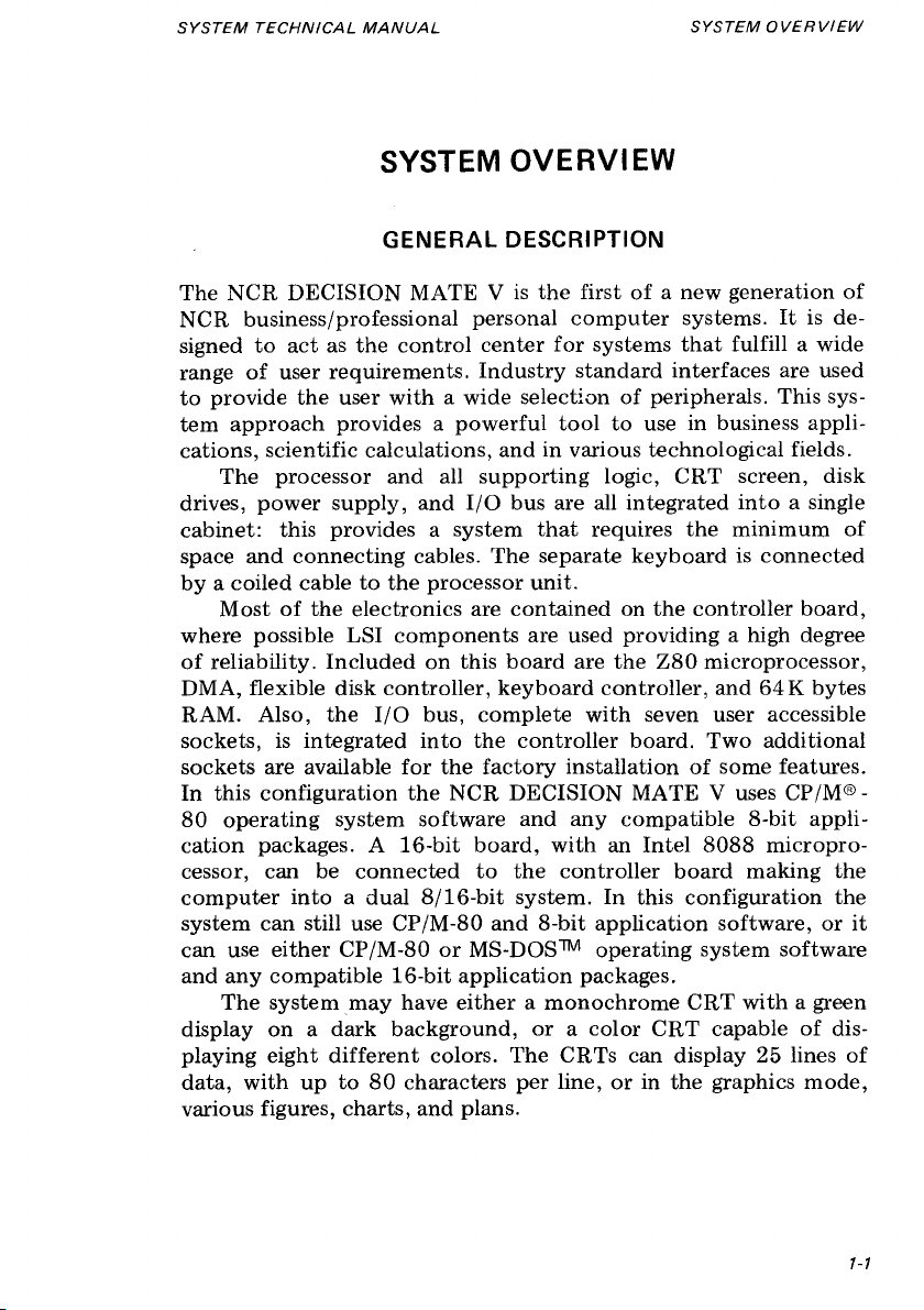
The NCR DECISION MATE V is the first of a new generation of
NCR business/professional personal computer systems. It is de
signed to act as the control center for systems that fulfill a wide
range of user requirements. Industry standard interfaces are used
to provide the user with a wide selection of peripherals. This sys
tem approach provides a powerful tool to use in business appli
cations, scientific calculations, and in various technological fields.
The processor and all supporting logic, CRT screen, disk
drives, power supply, and I/O bus are all integrated into a single
cabinet: this provides a system that requires the minimum of
space and connecting cables. The separate keyboard is connected
by a coiled cable to the processor unit.
Most of the electronics are contained on the controller board,
where possible LSI components are used providing a high degree
of reliability. Included on this board are the Z80 microprocessor,
DMA, flexible disk controller, keyboard controller, and 64 K bytes
RAM. Also, the I/O bus, complete with seven user accessible
sockets, is integrated into the controller board. Two additional
sockets are available for the factory installation of some features.
In this configuration the NCR DECISION MATE V uses CP/M® -
80 operating system software and any compatible 8-bit appli
cation packages. A 16-bit board, with an Intel 8088 micropro
cessor, can be connected to the controller board making the
computer into a dual 8/16-bit system. In this configuration the
system can still use CP/M-80 and 8-bit application software, or it
can use either CP/M-80 or MS-DOS™ operating system software
and any compatible 16-bit application packages.
The system may have either a monochrome CRT with a green
display on a dark background, or a color CRT capable of dis
playing eight different colors. The CRTs can display 25 lines of
data, with up to 80 characters per line, or in the graphics mode,
various figures, charts, and plans.
1-1
Page 8
7-2
For ex ample
freestandin g Winchester
Disk (10MB)
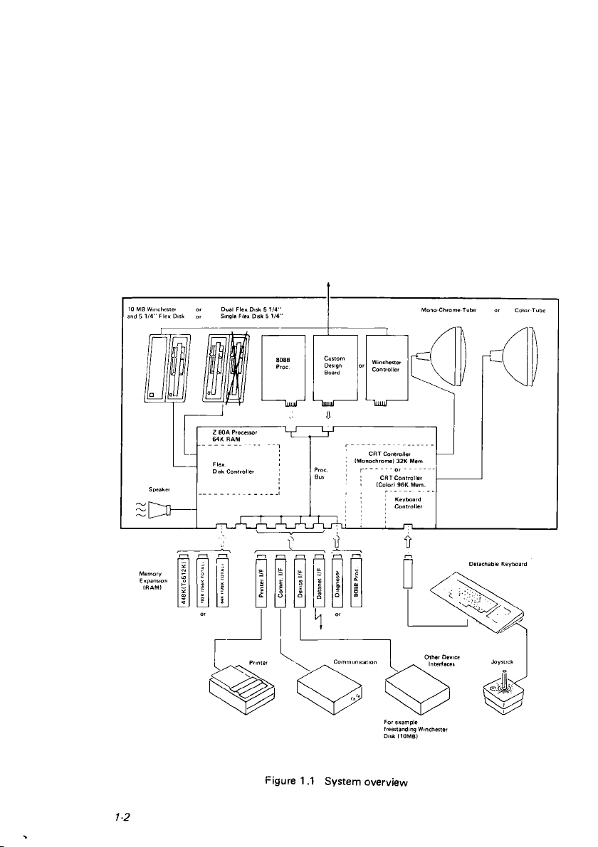
Figure 1.1 System overview
Page 9
SYSTEM TECHNICAL MANUAL
SYSTEM OV ER VIEW
The integrated disk drives are available in the following combi
nations:
• One 5 1/4-inch flexible disk drive
• Two 5 1/4-inch flexible disk drives
• One 5 1/4-inch flexible disk drive and one 5 1/4-inch fixed
Winchester disk drive
The I/O bus is an integral part of the controller board; it in
cludes seven sockets that allow the user to connect the various
peripheral adapters and options to the bus. These adapters and
options all use a common style of housing, permitting flexibility
in configuring the hardware. The cabinet design is such that the
adapters/options are fully recessed into the rear of the cabinet
when installed. The adapters/options do not require any pre
paration and can be plugged directly into the bus by the user.
The peripheral adapters are used to connect industry standard
printers, modems, and terminals to the bus. The bus is also used
for the connection of the memory expansion modules and other
special purpose modules.
Different versions of a “switcher” type power supply are used
depending on the power requirements of the different models of
the NCR DECISION MATE V. The power supply also provides
logical voltages to the bus for use by the peripheral adapters and
options.
NCR DECISION NET
The NCR DECISION NET System is a local area network system,
typically consisting of the following components:
» An NCR MODUS File Sharer
• An NCR OMNINET local area network
• A number of NCR DECISION MATE V personal computers
(up to 63)
To connect an NCR DECISION MATE V into the NCR
DECISION NET System, a special adapter, known as a transporter,
is required. This transporter (3273-K600) connects directly into
an I/O bus slot at the rear of the NCR DECISION MATE V.
1-3
Page 10

KIT DESCRIPTIONS
Various kits are available to enhance the capabilities or change the
hardware configuration of the NCR DECISION MATE V. Many of
these kits can be plugged directly into the I/O bus by the user:
others require installation by a service engineer.
Integrated Fixed Disk
This kit (K012) provides for the integration of a fixed (Winchester)
disk drive. The kit includes the necessary changes for the power
supply. When installed, the system has one fixed disk drive
(capacity 10M bytes) and one flexible disk drive (capacity 320/
360K bytes).
Second Integrated Flexible Disk
These kits upgrade an NCR DECISION MATE V from a system
with one flexible disk drive to a system with two flexible disk
drives. Kit K018 is for systems produced in the DIN color scheme,
kit K019 is for systems in the Corporate Appearance Plan (CAP)
color scheme.
Memory Expansion Modules
These kits (K200, 202, and 208) can be installed, by the user,
directly into slot 1 of the I/O bus. It is only possible to install
one kit into a system. The kits provide the following memory
capacities:
• K200 increases memory capacity from 64K to 128 K bytes
• K202 increases memory capacity from 64K to 256Kbytes
• K208 increases memory capacity from 64K to 512Kbytes
Centronics Peripheral Adapter
This kit (K210) can be installed, by the user, directly into the
I/O bus (slots 2 to 6). The kit includes a 2 metre (6.6 ft.) cable
complete with plug, that allows connection to a Centronics com
patible (parallel input) printer.
RS-232-C (Communications) Peripheral Adapter
This kit (K211) can be installed, by the user, directly into the
I/O bus (slots 2 to 6). The kit includes a 2 metre (6.6 ft.) cable
complete with plug, that allows connection to an RS-232-C com
patible (serial) communications device.
1-4
Page 11
SYSTEM TECHNIC AL MA NU AL
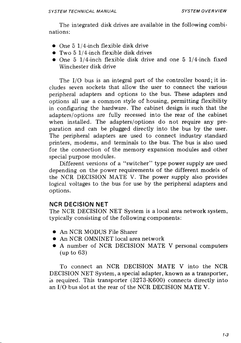
RS-232-C (Printer) Peripheral Adapter
SYSTEM O VER VIE W
This kit (K212) is similar to K211, but is used for the connection
of RS-232-C compatible (serial) printers.
RS-232-C (Plotter) Peripheral Adapter
This kit (K213) is used for the connection of a compatible plotter
(e.g. NCR 5403) to the NCR DECISION MATE V.
Blank Interface Adapters
These kits (K214, 217, and 218) comprise a housing, an I/O
bus connector, and a blank printed circuit board. They provide
the necessary hardware to help the system integrator to develop
custom interfaces or adapters.
• K214 provides hardware for one adapter
• K217 provides hardware for five adapters
• K218 provides hardware for 25 adapters
Integrated Modem
This kit (K219) can be installed, by the user, directly into the
I/O bus (slots 2 to 6). It is designed to support the following
modems:
® Bell 103 (300 baud)
® Bell 2035 (1200 baud)
Built into the modem housing are two sockets for the connec
tion of standard telephone type plugs: a cable is included for the
connection of a telephone.
Diagnostic Module
This module (K220) can be installed directly into slot 7 of the I/O
bus, and is intended for service engineers and other persons inter
ested in diagnosing problems. The module tests the computer and
provides information on failures. It also monitors the logical
voltages (+5 and +12 Vdc) and indicates whether the voltages are
within or outside the specified limits. For a full description, refer
to the NCR DECISION MATE V Service Manual.
8/1 6-Bit Processor
Kit K231 can be installed, by the user, directly into slot 7 of the
I/O bus. It converts the NCR DECISION MATE V from an 8-bit
system to a dual 8/16-bit system that is capable of using either
8-bit or 16-bit operating system and application software.
1-5
Page 12
Kit 230 functions similarly to K231, but is connected inter
nally to the controller board. This kit should be installed by a
field engineer; it is not suitable for installation by the user.
Tilt Mechanism
This kit (K240) provides a means of tilting the NCR DECISION
MATE V by seven degrees. The user can easily install the device
by fixing a base plate to the bottom of the computer, using the
existing holes in the base of the cabinet.
NCR OMN IN ET Transporter
This kit (K600) can be installed, by the user, directly into the
I/O bus (slots 2 to 6). The adapter has twice the thickness of
other adapters, therefore it requires two slot positions for installa
tion. The adapter provides the interface between the NCR DE
CISION MATE V and the DECISION NET System.
MODEL AND KIT ID ENTIFICATION
The configuration of the hardware is defined by the model num
ber. The standard arrangement of the model number is shown
below:
3 2 7 3 - x x
x x - x x x x
Language code
Power code
Sub model
Ma jor model
NCR class number
The model number of the NCR DECISION MATE V is shown
in Figure 1.2. The optional features are shown in Figure 1.3. An
asterisk indicates a planned development not released at the time
of printing, but included for reference.
1-6
Page 13
SYSTEM TECHNIC AL MANU AL
SYSTEM O VER VIEW
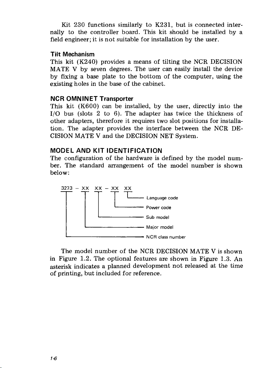
Class 3273
Major Model 01
Sub-Model 01
Power Code 60 120 V, 5 0/ 60 Hz
Language Code
NCR Class Number
8- bit Proc ./1 2" CRT Monochrome
11 8 /1 6-bit Proc./12 " CR T Monochrom e
12
8 /1 6-bit Pr oc ./12" CR T Color
One 5 1 /4 " Flex Disk Drive
Tw o 5 1/ 4" Flex Disk Drives
02
One 5 1 /4 " Flex Disk Drive and one
03
5 1/ 4" W inchester Fixe d Disk
220 V, 5 0/ 60Hz
65
70
74 230 V , 5 0/6 0Hz
75 240 V, 50 /6 0Hz
00
01
02
03
04 Portuguese
05
06
07 Du tch
08
09
42
10 0V, 5 0/6 0Hz
US English
Intern ation al English
UK English
Spanish
French
German
Flemish
Swedish
Danish
10
11 Norwegian
12
Italian
Greek
13
Yugoslavian
14
Japanese/Katakana
15 *
Taiwanese
16 *
17 * Ar abic
Iranian
18 *
19 * Hebrew
20 Finnish
25
33
40 Swiss
La tin American/S panish
Canadian
South African
* Not y et released bu t shown for reference purposes
Figure 1.2 M odel number description
1-7
Page 14
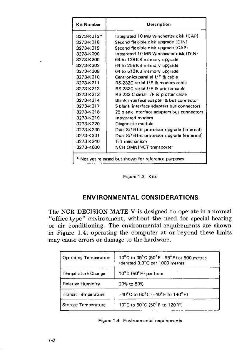
K it Number
De scriptio n
3273-K 01 2*
32 73-K0 18
32 73-K019
32 73-K0 90
32 73-K2 00
32 73-K2 02 64 to 25 6KB memory upgrade
32 73-K2 08
32 73-K2 10
32 73-K211
32 73-K2 12 RS-232C serial l/F & printe r cable
32 73-K2 13
32 73-K2 14 Blank inte rfac e adap ter & bus c onn ector
32 73-K217 5 b lan k interface adapters bus connectors
32 73-K2 18
32 73- K219
32 73-K2 20
32 73- K230
3273-K231
32 73-K2 40
32 73-K6 00
* Not y et released b ut shown for reference purposes
Inte grated 10 MB Winchester d isk (CAP)
Second flex ib le disk upgrade (D IN)
Second flex ib le disk upgrade (CAP)
Inte grated 10 MB Winchester disk (DIN)
64 to 12 8K B memory upgrade
64 to 512KB memor y upgrade
Centronics para llel l/ F & cable
RS-232C serial l/F & modem cable
RS-232-C serial l/F & plott er cable
25 blan k interface adapters bus connectors
Inte grated modem
Dia gnostic modu le
Dual 8/1 6-bit processor upgrade (intern al)
Dual 8/1 6-bit processor upgrade (externa l)
T ilt mechanism
NCR OM NINE T transp orter
Figure 1.3 Kits
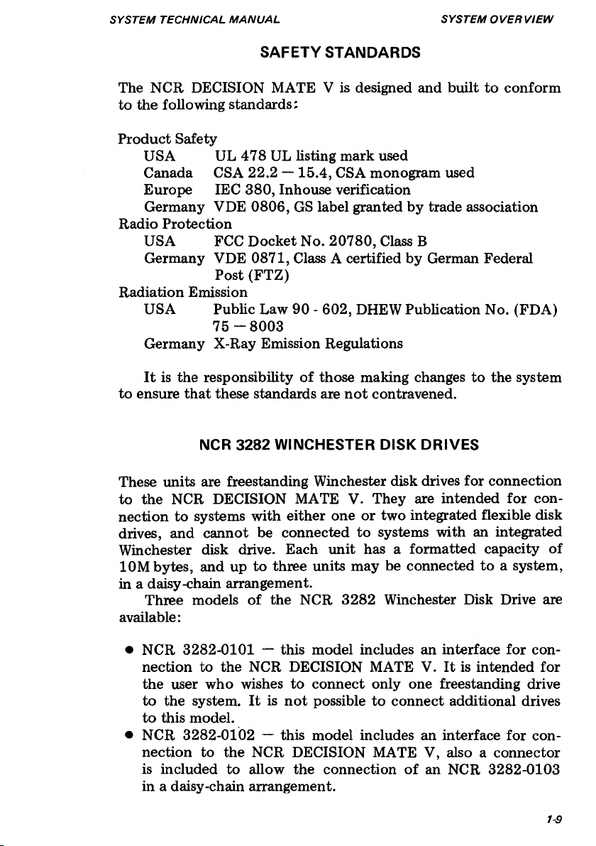
ENV IRO N MENT AL CONS IDERAT IONS
The NCR DECISION MATE V is designed to operate in a normal
“office-type” environment, without the need for special heating
or air conditioning. The environmental requirements are shown
in Figure 1.4; operating the computer at or beyond these limits
may cause errors or damage to the hardware.
Operatin g Tem perature
Temperatu re Change 10°C (50°F ) per hour
Relative Hum idity 20% to 80%
Trans it Temperature
Storage Tem perature 10°C to 50 °C (50°F to 1 2 0°F)
Figure 1.4 E nv ironme nta l requirements
1-8
10°C to 35 °C (50°F - 95° F) at 500 metres
(derated 3.3° C per 1000 metres)
-4 0° C to 60° C (-40 ° F to 140 °F)
Page 15
SYSTEM TECHNICAL M ANUAL
SAFETY STAND ARDS
SYSTEM OVERVIEW
The NCR DECISION MATE V is designed and built to conform
to the following standards:
Product Safety
USA UL 478 UL listing mark used
Canada CSA 22.2 — 15.4, CSA monogram used
Europe IEC 380, Inhouse verification
Germany VDE 0806, GS label granted by trade association
Radio Protection
USA FCC Docket No. 20780, Class B
Germany VDE 0871, Class A certified by German Federal
Post (FTZ)
Radiation Emission
USA Public Law 90 - 602, DHEW Publication No. (FDA)
7 5 -80 0 3
Germany X-Ray Emission Regulations
It is the responsibility of those making changes to the system
to ensure that these standards are not contravened.
NCR 3282 W INCHESTER DISK DRIVES
These units are freestanding Winchester disk drives for connection
to the NCR DECISION MATE V. They are intended for con
nection to systems with either one or two integrated flexible disk
drives, and cannot be connected to systems with an integrated
Winchester disk drive. Each unit has a formatted capacity of
10M bytes, and up to three units may be connected to a system,
in a daisy-chain arrangement.
Three models of the NCR 3282 Winchester Disk Drive are
available:
• NCR 3282-0101 — this model includes an interface for con
nection to the NCR DECISION MATE V. It is intended for
the user who wishes to connect only one freestanding drive
to the system. It is not possible to connect additional drives
to this model.
• NCR 3282-0102 — this model includes an interface for con
nection to the NCR DECISION MATE V, also a connector
is included to allow the connection of an NCR 3282-0103
in a daisy-chain arrangement.
1-9
Page 16
• NCR 3282-0103 — this model connects to the NCR 3282-
0102 and also has a connector permitting the connection
of another NCR 3282-0103.
All models are supplied with a cabinet that includes the drive,
power supply, fan, power cables, and the appropriate intercon
nection cables to provide for easy assembly of the units in a daisy-
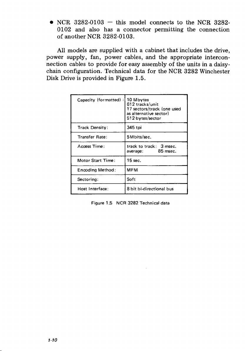
chain configuration. Technical data for the NCR 3282 Winchester
Disk Drive is provided in Figure 1.5.
Capacity (fo rm atted ) :
Tra ck De nsity: 345 t pi
Tra nsfe r Rate:
Access Tim e: tra ck to trac k: 3 msec.
M otor Start Tim e: 15 sec.
Encoding Me th od:
Sectoring: Soft
Host Interface: 8 b it bi-direction al bus
Figure 1.5 NCR 3 282 Technical data
10 Mbytes
612 trac ks /u nit
17 s ectors/track (one used
as alternative sector)
512 bytes/sector
5M bits /se c.
average: 85 msec.
MF M
1-10
Page 17
SYSTEM TECHNICAL MANUAL
HARDWARE DESCRIPTION
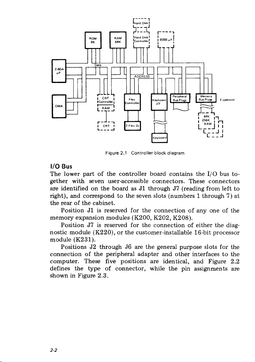
CONTR OLLER MODULE
HARDWARE DESCRIPTION
The controller module consists of two printed circuit boards, the
controller board and the graphics controller board. Two types of
graphic controller boards are used: one, with 32Kbytes of RAM
for systems with a monochrome CRT, the other, with 96 Kbytes
of RAM for systems with color CRT.
CON TROLL ER BOARD
The controller is a 300mm x 290mm printed circuit board and
utilizes a Z80A microprocessor and auxiliary logic to drive and
control a family of 8-bit common memory and peripheral modules.
Figure 2.1 shows a block diagram of the controller board.
• Z80A microprocessor is operated with a 4 MHz clock.
• The LSI flexible disk controller contains the circuitry and con
trol functions for interfacing one or two flexible disk drives. It
is capable of supporting double density format including
double sided recording. Hand shaking signals are provided
which make DMA operation easy to incorporate with the aid
of the DMA controller integrated circuit.
• The RAM controller provides mulitplexed addresses and ad
dress strobes, as well as refresh access arbitration for the
64 Kbytes dynamic RAM contained on the controller board,
and also for the memory expansion modules. (Up to a maxi
mum of 256Kbytes, or 512Kbytes with the multi-layer con
troller board).
• The loudspeaker is designed to produce tones for keyboard
acceptance click, bell, and music demonstration. A separate
circuit provides the frequencies from 110Hz to 1174.7Hz. The
small audio speaker is housed on the controller board. The
loudness is adjusted by a user-accessible potentiometer.
• The keyboard interface connects the ASCII encoded keyboard
to the controller board by a four-wire cable carrying logic
ground, frame ground, +5V, and data signal. The keyboard is
polled by the controller. When a key is pressed, the serial
data is returned on the same line. For a detailed description
see the keyboard description.
2-1
Page 18
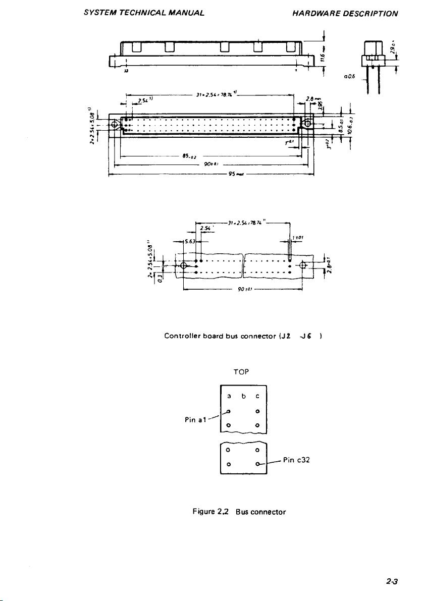
I/O Bus
The lower part of the controller board contains the I/O bus to
gether with seven user-accessible connectors. These connectors
are identified on the board as J1 through J7 (reading from left to
right), and correspond to the seven slots (numbers 1 through 7) at
the rear of the cabinet.
Position J1 is reserved for the connection of any one of the
memory expansion modules (K200, K202, K208).
Position J7 is reserved for the connection of either the diag
nostic module (K220), or the customer-installable 16-bit processor
module (K231).
Positions J2 through J6 are the general purpose slots for the
connection of the peripheral adapter and other interfaces to the
computer. These five positions are identical, and Figure 2.2
defines the type of connector, while the pin assignments are
shown in Figure 2.3.
2-2
Page 19
SYSTEM TECHNICAL MANUAL
HARDWARE DESCRIPTION
Con tro ller board bus connector (JZ ^1 S )
Figure 2.2 Bus connector
Page 20
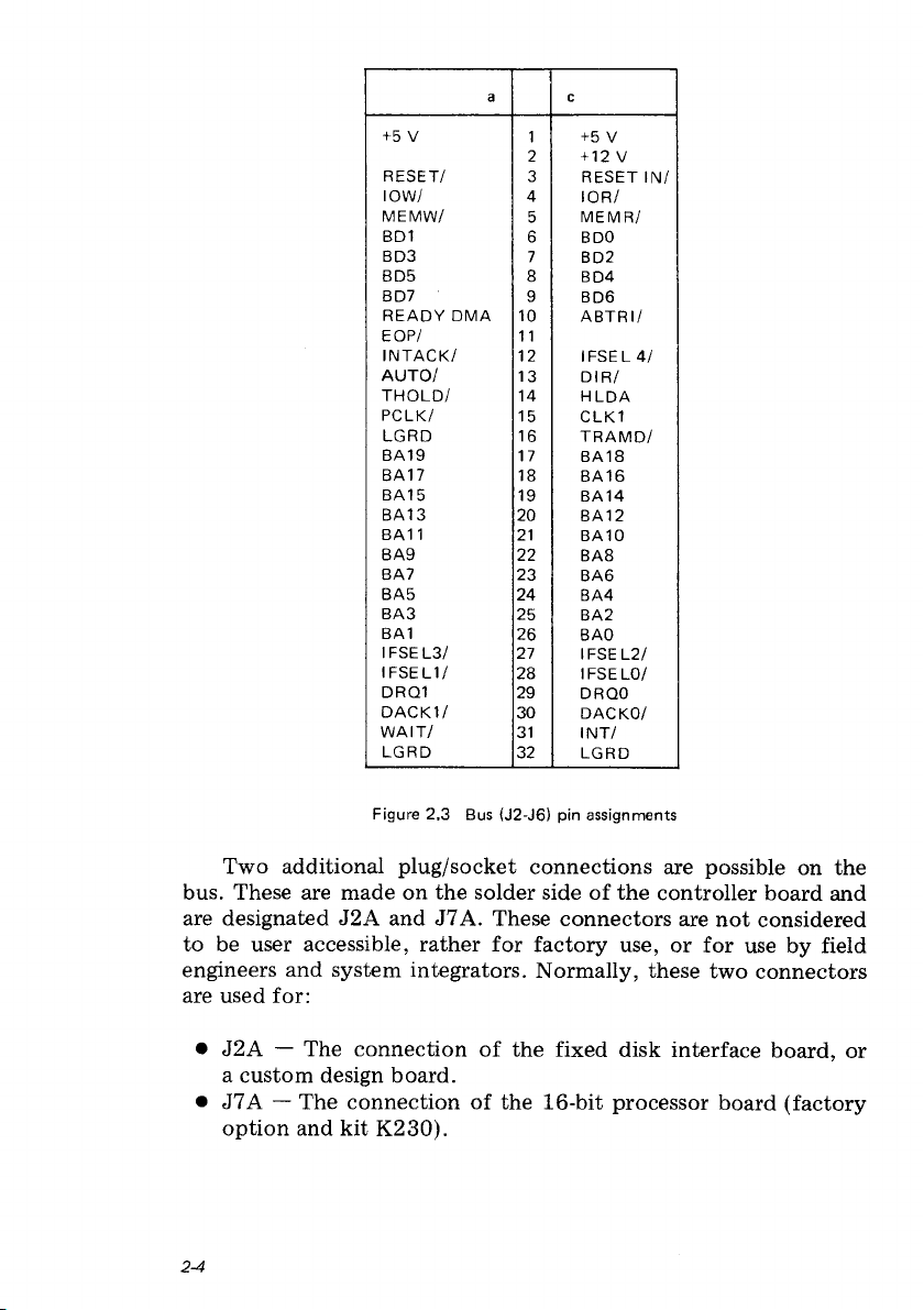
a
c
+5 V
RESET/ 3
IOW / 4
ME MW/
BD1
BD3
BD5
BD7
REA DY DM A
EOP / 11
IN TA CK/ 12
AUT O/
THO LD / 14
PC LK/
LG RD
BA 19
BA 17
BA1 5
BA13
B A11 21
BA 9
BA7
BA 5
BA 3
BA1
IF SE L3 / 27
IF SE L1/
DRQ1
DAC K1/ 30
W AIT /
LG RD
20
22
23
24
25 BA2
26 BAO
28
29
31
32
1 +5 V
2
+ 12 V
RESET IN /
I OR /
5 ME M R/
6 BDO
7 BD2
8 BD4
9
BD6
10
A BTR I/
IFSEL 4/
13 D IR /
H LD A
15
CLK1
16
TRAM D/
17
BA 18
18
BA1 6
19 BA 14
BA1 2
BA 10
BA 8
BA 6
BA4
IF SE L2/
IFSELO/
DRQO
DA CK O/
I NT /
LG RD
Figure 2.3 Bus (J2-J6) pin assignments
Two additional plug/socket connections are possible on the
bus. These are made on the solder side of the controller board and
are designated J2A and J7A. These connectors are not considered
to be user accessible, rather for factory use, or for use by field
engineers and system integrators. Normally, these two connectors
are used for:
• J2A — The connection of the fixed disk interface board, or
a custom design board.
• J7A — The connection of the 16-bit processor board (factory
option and kit K230).
2-4
Page 21
SYSTEM TECHNICAL MANUAL
HARDWARE DESCRIPTION
The power requirements for the I/O bus plugs are:
• For each peripheral plug + 5V ± 5% max. Current 0.5A
or
+12V ± 5% max. Current 0.1 A
• For all plugs (Jl, J2, J2A, J3, J4, J5, J6, J7 and J7A)
+ 5V + 5% max. 5.0A
+12V ± 5% max. 0.6A
The DC voltage levels for the I/O bus plugs are:
• Input/Output HIGH-Voltage V[j = 2.4 to 5.5 Volts
• Input/Output LOW-Voltage Vl = -0.5 to 0.8 Volts
Timing charts are provided in Figures 2.4 to 2.8.
2 5
Page 22
£
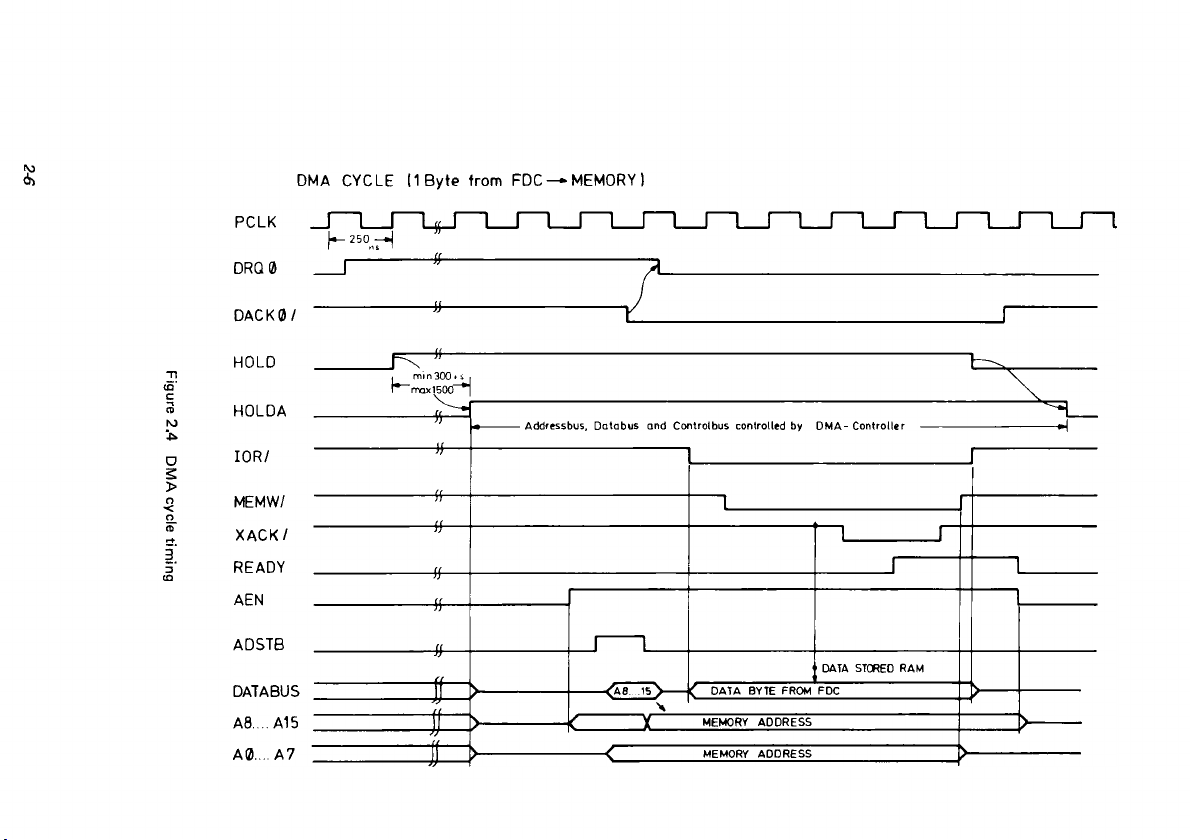
Figure 2.4 DMA cycle tim ing
DMA CYCLE CIByte from FDC — MEMORY)
Page 23
SY ST EM TE CH NICA L M A NU AL H AR DW AR E DES CR IPTIO N
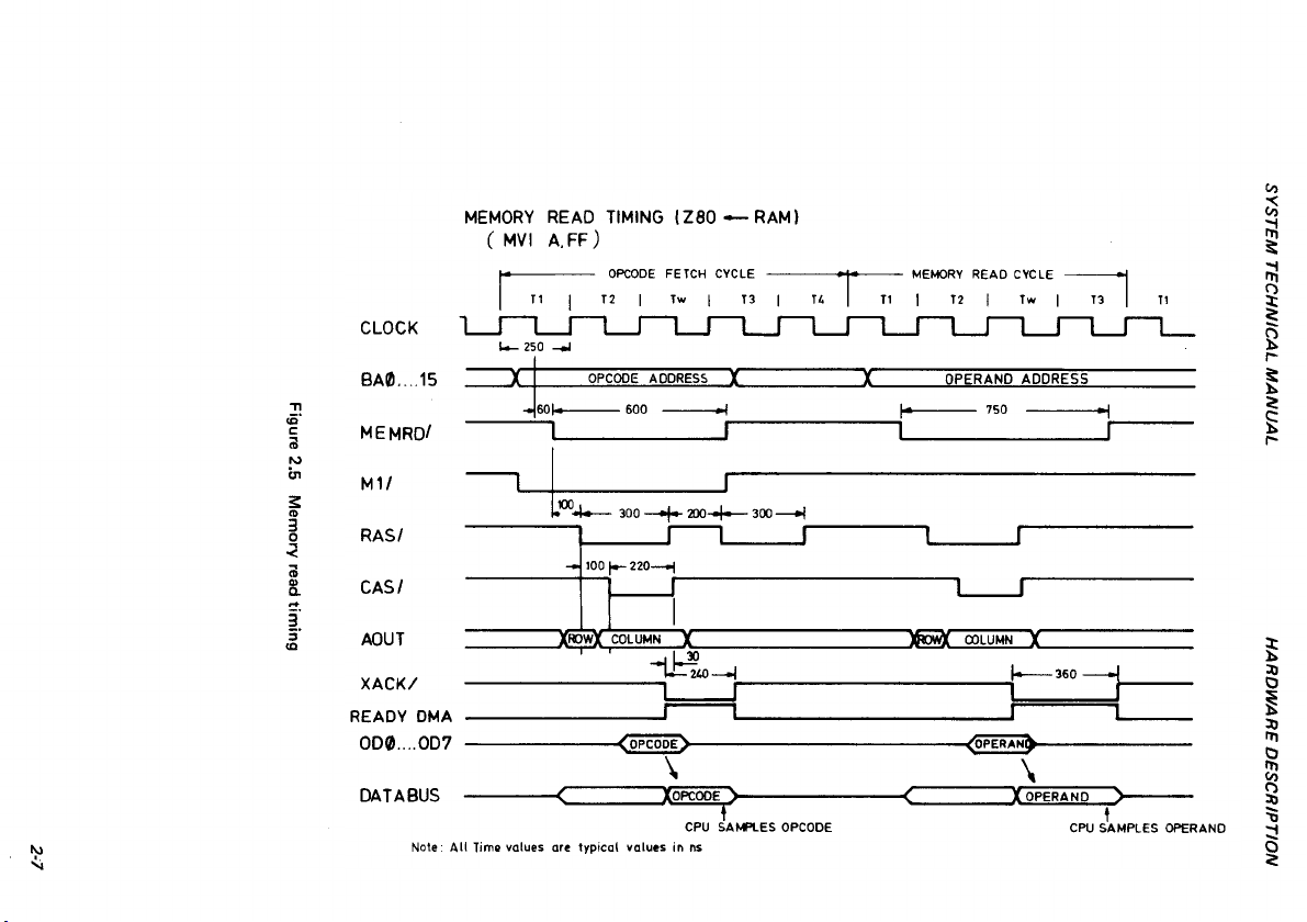
Figure 2.5 Me mory read tim ing
N>
•s i
Page 24
do
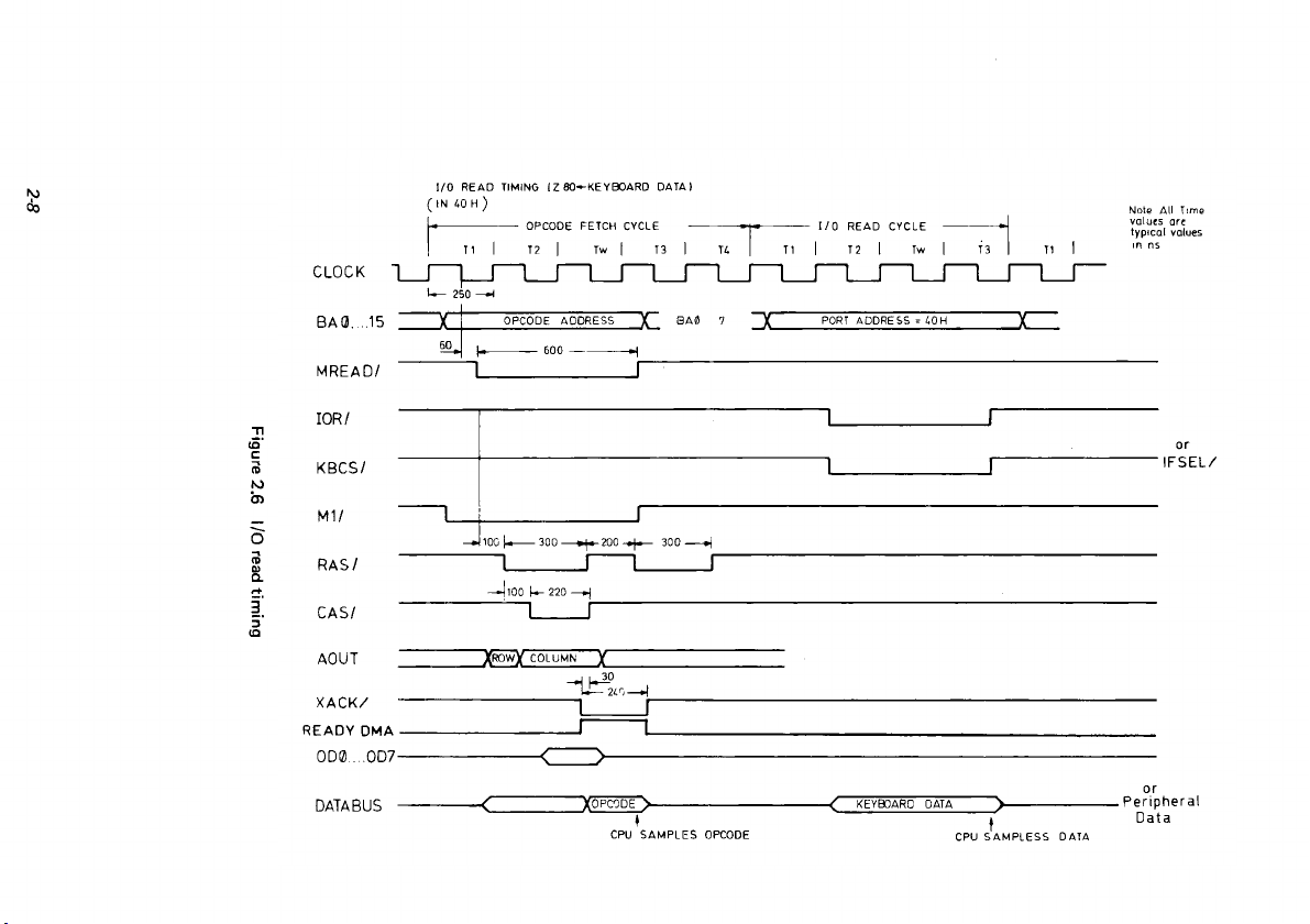
Figure 2.6 I/O read timing
Page 25
SY ST EM TE CH NICA L MAN UA L H AR DW AR E DESCRI PTION
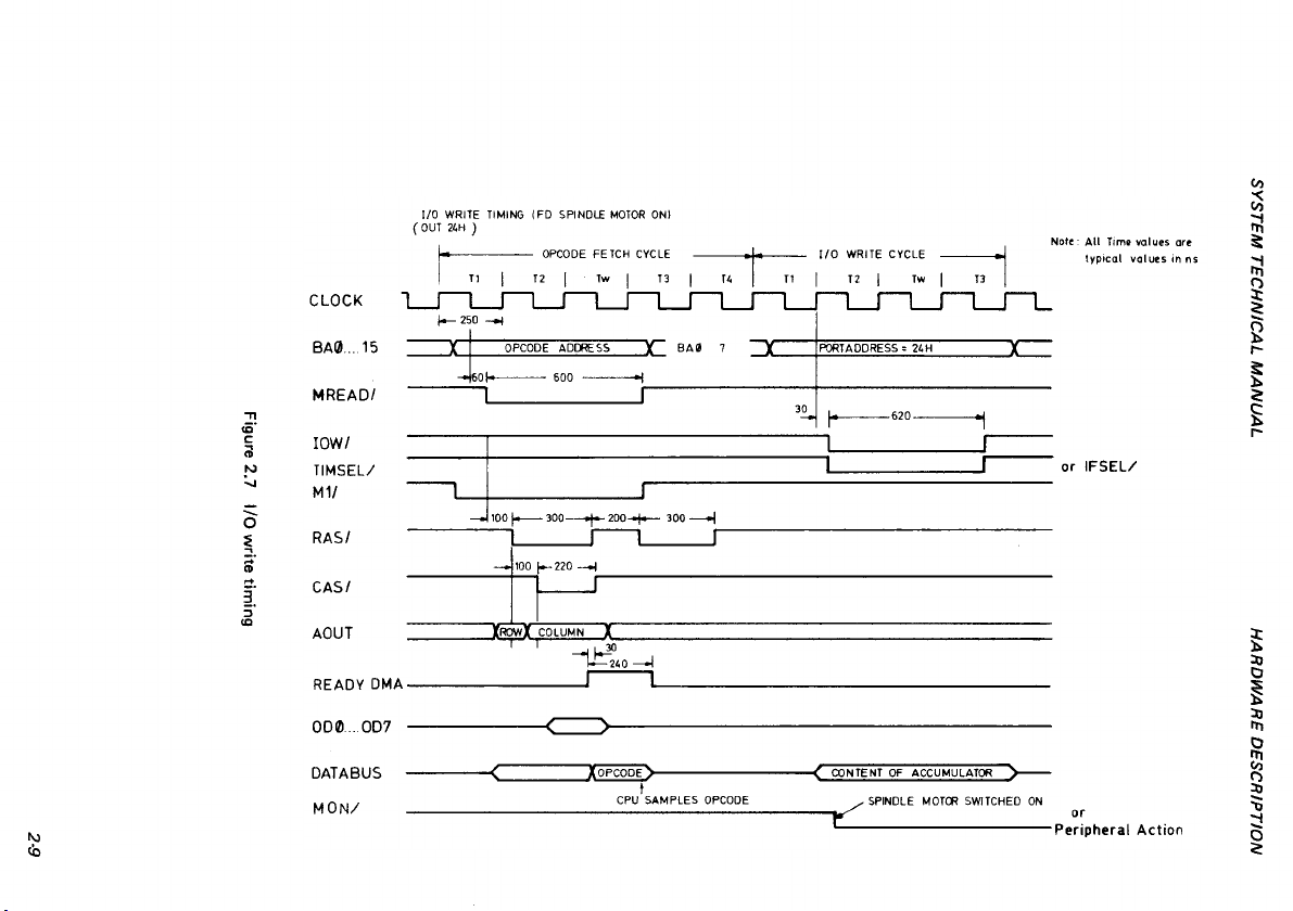
Figure 2.7 I/O w rite tinning
to
Page 26
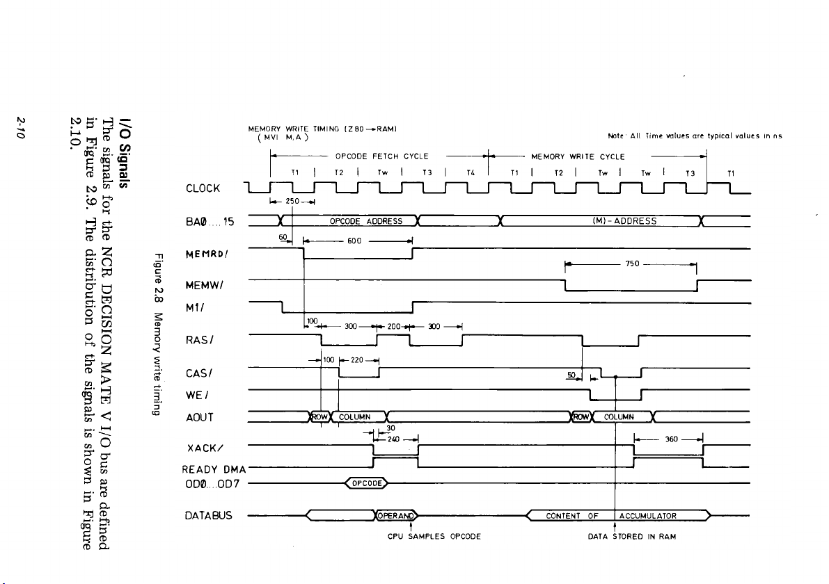
2- 10
in Figure 2.9. The distribution of the signals is shown in Figure
The signals for the NCR DECISION MATE V I/O bus are defined
2.10.
I/O Signals
Page 27
S Y S T EM T E C H N IC A L M A N U A L H A R D WA R E D E S C R IP TI O N
2-11
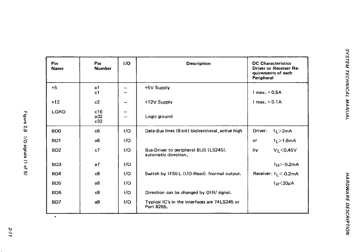
Pin Pin I /O
N am e N um ber
+ 5
+12
Fi gur e 2. 9 I /O signals (1 of 5)
LG R D
BD O c6
BD 1
B D2 c7
B D3
B D4 c8
B D5 a8 I/O
B D6 c9
B D7 a9
a1
c1
c2
c16
a 32
c3 2
a6
a7
_
—
-
_
—
I/ O
I/ O
I/ O
I/ O
I/ O
I/ O
I/ O
+ 5V Su pp ly
+ 12 V Su pp ly
Lo gic grou nd
Data -Bu s lines (8 -b it) bidirection al, a ctive hig h D river: l|_ >2m A
Bus- Driver t o p eri ph era l BU S (LS 2 45 ),
a ut om atic d ire ct ion .
S witch by IF S E L (I/O -Rea d ). N orma l ou tp ut .
D ire cti on can be ch anged by D IR / s igna l.
Typ ical IC 's in th e interfac es are 74L S 24 5 or
Port 82 5 5.
D escri pt ion D C C harac ter istics
D riv er o r Re ceiver Re
quir em en ts of each
Pe ripher al
I m ax . = 0 .5 A
I m ax . = 0 .1 A
or I l > 1.6m A
by V l < 0 .4 5 V
l| -|> -0 .2 m A
Re cei ver : l[ _< -0 .2 m A
l( -l< 2 0pA
Page 28
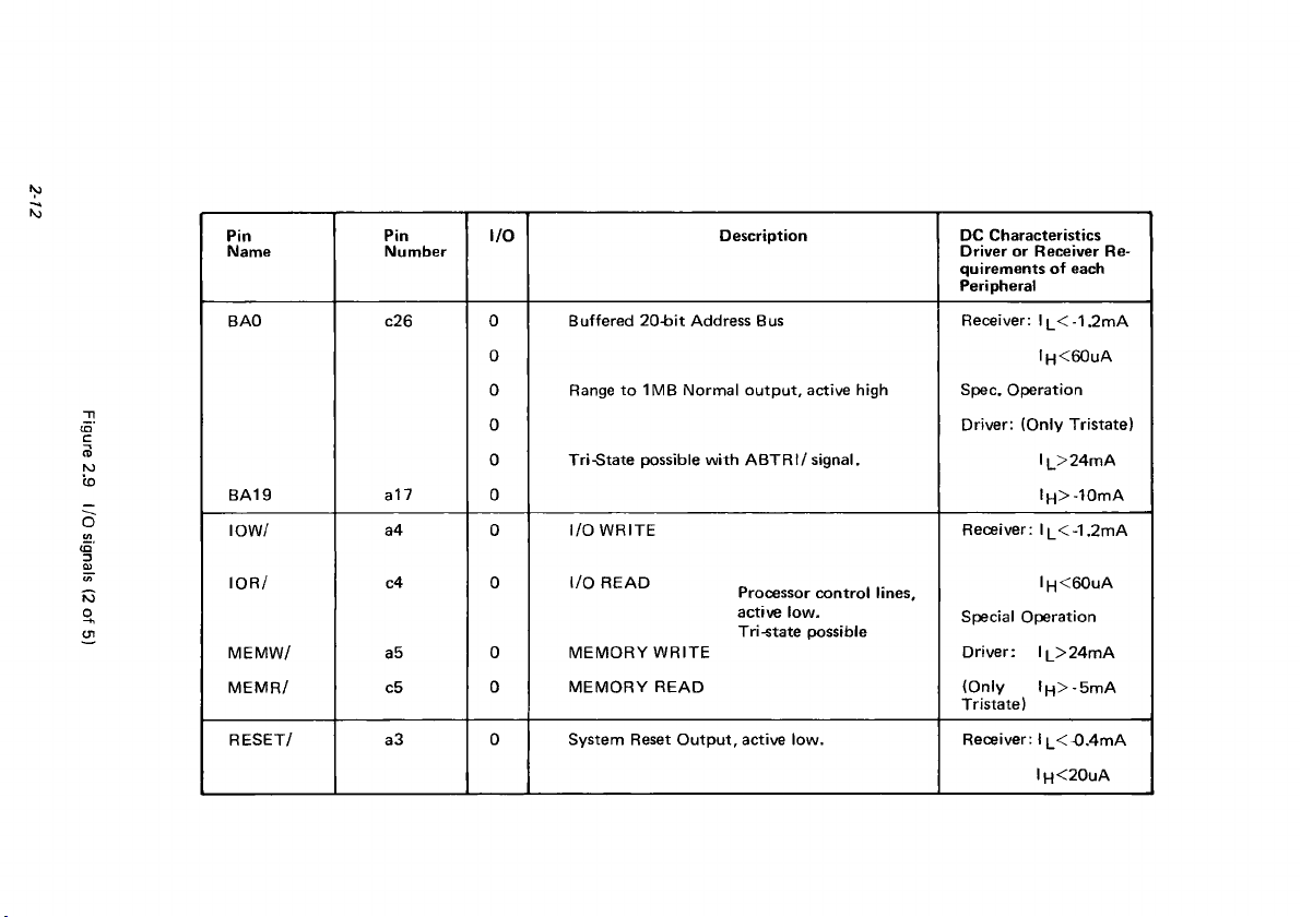
2- 12
Pin
Name N um ber
BAO
Figure 2.9 I/O signals (2 o f 5)
BA 19
IOW/
IO R/
ME MW/
M EM R/ c5 0
RE SE T/
Pin
c26
a17
a4
c4
a5 0
a3 0 System Reset Outp ut, active low . Receiver: I (_<-0.4mA
I/O
0
0
0
0
0
0 l|-l> -10m A
0 I/O WRITE
0 I/O RE AD _ .. .
Bu ffered 20 -bit Address Bus Receiver: l|_< -1.2m A
Range to 1MB Normal ou tput, ac tive high Spec. Op eration
Tri-State possible with A BTR I/s igna l.
MEMOR Y WRITE Driver: l|_ >24mA
MEMOR Y READ
Description DC Characteristics
Processor c on tro l lines.
active low .
Tri-sta te possible
Dr iver o r Receiver Re-
quirem en ts o f each
Peripheral
l(- l<6 0uA
Drive r: (Only Tris tate)
I |_>24mA
Receiver: IL <- 1.2m A
l|- l<60 uA
Special Operation
(O nly l(-) >- 5m A
Trista te)
Ih < 2 0uA
Page 29
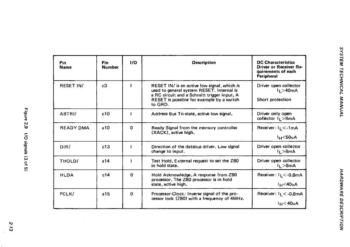
SYSTEM TECHNICAL MANUAL HARDWARE DESCRIPTION
Pin
Name
RESET IN/ c3 1
Figure 2.9 I/O signals (3 o f 5)
A B TRI / c10 1
REA DY D MA a10 0
DIR /
THOL D/
H LD A
PCLK/ a1 5 0
2 -1 3
Pin
Nu mber
c13 1
a14
c14
I/O
1
0
RESET IN / is an active low signal, wh ich is
used to general system RESET. Internal is
a RC c irc uit and a S ch m itt trigger inp ut. A
RESET is possible for example by a switch
to G R D .
Address Bus Tri-state, active low signal.
Ready Signal fro m the mem ory contr oller
(X AC K), active high.
Direc tion of th e databus d riv er. Low signal
change to inp ut.
Test Ho ld. External request to set the Z8 0
in hold state.
Ho ld Acknow led ge. A response fro m Z80
processor. The Z80 processor is in hold
state, active high.
Processor-Clock: Inverse signal of th e pro
cessor lock (Z80) with a freq uency o f 4 MH z.
Description
DC Cha racteristics
Drive r o r Receiver Re
quirem en ts of each
Peripheral
Driver open collector
Sh ort pro tectio n
Driver o nly open
co lle ctor l[_> 8m A
Receiver: l|_< -1mA
Driver open co llec tor
Driver open collector
Receiver: l|_ <-0.8m A
Receiver: l|_<-0.8m A
1 |_>40m A
I(-I<50uA
I L>8 m A
I [_>8m A
I h <40uA
l|- )< 40u A
Page 30

2 -1 4
Pin
Name
C LK 1/ c15 0 Clock o utput 1 MH z.
Pin
Nu mber
I/O Description
DC Characteristics
Dr iver o r Receiver Re
quirem en ts of each
Peripheral
I l < -0.8m A
Ih < 4 0 uA
Figure 2.9 I/O signals (4 o f 5)
TR AMD/
c16 I Test RA M-D isable. F or external ROM or RAM
ex tension. S witching w ith the system RA M.
The RA M ou tp ut w ill be disabled. Used b y the
Dia gno stic m odu le. The signal is active low .
I NT / c31 I INTE RR UPT. In terru pt for Z80 , active low. D rive r on ly, open
IN TA CK/ a12 0
IN TE RR UPT ACKNOW LE DG E from the Z80
Processor, active low.
Dr iver o nly, open
co lle cto r l|_>8 m A
co lle cto r I (_> 8mA
Receiver: li_<-1.2 mA
I|-I< 60 uA
W AIT/ a31
DRQO c29
DRQ1
a 29 1
I W AIT/ set the Z80, 8088, and DM A co ntr oller
in Wait-State (not ready ), active lo w
1
DM A-R equest for Channel 0, active high Driv er on ly Tristate
DMA Request for C hannel 1, active high.
As ynchro nou s channel request inpu ts are used
by peripherals t o request DM A service.
DA CKO/ c3 0 0 DM A-Ackn owledge Channel 0, a ctive low .
DACK1 / a 30 0 DM A-A cknow led ge Channel 1, a ctive low . These
lines in dicate an active DM A channel.
Driver o nly, open
co lle cto r l|_ >8 mA
I h > -2m A
I i_>2m A
Receiver: l[_<-0.5 mA
IH < 2 0uA
Page 31

SYSTEM TECHNICAL MANUAL HARDWARE DESCRIPTION
Pin
Name
EOP / a1 1
Figure 2.9 I/O signals (5 of 5)
IFSELO/ c28 0 Interfa ce select 0 to 4, activ e low .
IF SE L1/ a28 0 The Interfa ce does no t need o wn address
IFSE L2/ c27 0
IF SE L3/ a27 0 is made by any IFSEL and BA 3 (B A3 /).
IF SE L4/ c1 2 0 (10 Periphera ls). Au tom atic change of th e data
A UTO /
2 -1 5
Pin
Nu mber
a13
I/O
I/O
Description
End o f Process-EOP signals tha t DM A service has
been com ple ted. A lso in pu t active low.
Fo r details 8237 A-5 Spec.
decoder.
The Select of the I/O ports in the perip herals
bus dir ec tio n. This change is not possible w hile
a D MA fun ct ion is being p erform ed.
Change perip heral fro m board type 1 to board
type 2. N ot connected on board typ e 1.
DC Cha racteristics
Dr iver o r Receiver Re
qu irements of each
Peripheral
Receiver: 11_<-0.4mA
lH <2 0uA
only for 3 Peripherals
Drive r open Collec tor
I |_> 5mA
Receiver:
I l < -0.8mA
Ih <40 uA
Receiver: l|_< 1.2mA
I h < 60/uA
Pu ll-up resistor
1-10 Koh m to +5 V
Page 32

2-16
Figure 2.1 0 Signal dis tri bu tio n
Page 33

SYSTEM TECHNICAL MANUAL
Interface Configuration
HARDWARE DESCRIPTION
The configuration of the I/O interface and information on the
interface select signals is provided in Figure 2.11.
Figure 2.11 In terface configu ration
2-17
Page 34

GRAPHICS CO NTROLLER BOARD
With the 32Kbytes of graphics memory, the system can create a
640 x 400 resolution image. Upper and lower case characters are
displayed in a 6 x 9 dot pattern on a 8 x 16 dot matrix which
allows for descended lower case characters. The graphic controller
operates in mixed mode. It can draw the following figures: hori
zontal and vertical lines, vectors, rectangles, arcs, circles, graphic
character symbols, line pattern or area pattern, and slanted figures
(+n x 45). Also, the CRT controller supports scrolling, zooming
set mask, reset mask, replace complement and clear screen. Re
verse and normal video, blink attribute and half intensity are also
available. (See NEC 7220 data sheets)
The graphics controller board is connected directly onto the
controller board with two connectors, J/P 113, and J/P 114. The
pin assignments for these connectors are shown in Figure 2.12.
Pin assignments P114
Figure 2.12 G raphic co ntroller connectio ns
Pin assignments P113
The graphics controller board for color systems has a memory
capacity of 96Kbytes, and can display eight colors — black, white,
red, green, blue, yellow, magenta, and cyan.
In the text mode the characteristics are:
• 25 lines, 80 characters per line
• Characters in any of the eight colors
• Background in any of the eight colors
• Blinking attribute
2-18
Page 35

SYSTEM TECHNICAL MANUAL
In the graphics mode the characteristics are:
• Each dot position in any of the eight colors
• No attributes
HARDWARE DESCRIPTION
16-BIT PROCESSOR
•
The 16-bit processor can be installed in an NCR DECISION
MATE V, allowing the computer to function as either an 8- or
a 16-bit processor.
The 16-bit processor is availabe in two versions; both versions
function identically. The two versions are:
• A factory-installed feature (F230), or an engineer-installed
kit (K230); the board is connected to the solder side of the
controller board at P/J7A. This version is not installable by the
user.
• A self-contained module (K231) which the user can plug di
rectly into the controller bus at slot 7.
The configuration of the 16-bit processor board is:
• 8088 processor with 5 MHz clock
• Bus controller
• 4K x 8 PROM
• Spare socket for a co-processor (e.g. 8087)
• Switch logic for dual processor concept
Because the Z80A and the 8088 processor use the same bus,
only one processor will work at a time. The other processor is
in HOLD state. Both processors have equal rights and will perform
all memory and I/O operations.
Only the operating processor can perform switching to the
other processor.
The 16-bit processor operates in maximum mode.
Contents of the PROM:
Address range FF000-FFFFF
Start address after Reset FFFFO
Jump to start point of the operating system
Jump to start point of the operating system Level 0 diagnostic
2-19
Page 36

Figure 2.1 3 16 -bit processor timing
The processor timing of the 16-bit processor is shown in
Figure 2.13, and the pin assignments in Figure 2.14.
2-20
Page 37

SYSTEM TECHNICAL MANUAL
HARDWARE DESCRIPTION
Figure 2.14 1 6-b it processor pin assignments
POWER SUPPLY
The power supply comprises the following modules:
• Power connector
• Primary fuse
• Transformer
• Rectifier
• Switcher (+5V, +12V)
• 1 Secondary Fuse for unregulated output voltage
2-21
Page 38

The power supply is capable of operating with the following ac
power sources.
Frequency
Nominal Voltage
100
Range
9 0 -10 7
120 1 04 -1 27
49 to 61 Hz
220
19 8-23 5
230 207 - 246
240 21 6 -2 57
The average ac input wattage is 70W (Basic Model w/o periph
erals). The outputs of the standard power supply are:
Supply
+18V to +35V
+18V to +35V
Regulated
+ 5.1V± 3%
+12.2V+ 3%
Max. Current
10.0 A
3.2 A
Ripple
< 50mVpp
< 120mVpp
Models with hard/flexible disk combination require a larger
transformer and switcher assembly. The outputs of these are:
Supply
Regulated
Max. Current Ripple
+18V to +35V
+18V to +35V
+ 5.1V± 3%
+12.2V+ 3%
13.0 A
4.1 A
< 50mVpp
< 120mVpp
The color CRT also requires a larger transformer, but the
standard switcher and rectifier can be used for controller board,
flexible disks, keyboard, and I/Fs. The rectifier and switcher for
the color CRT are placed on the CRT board.
Output power requirements for the color CRT are:
Regulated Max. Current Ripple
107V±2V
2 -2 2
0.5 A <400mVpp
Page 39

SYSTEM TECHNICAL MA NUAL
HARDWARE DESCRIPTION
Current limiting and over voltage protection are provided. The
electrical power is enough for both the computer and its interfaces
and options, but printers and free-standing disk drives require their
own ac power source. The following power line transients should
not affect the specified performance:
Input Voltage
50% of nominal
Duration Frequency of Occurrence
1/2 cycle Once in 10 seconds
The power supply assembly is available in three models:
• For a power source with a nominal voltage of 120 Vac
• For a power source with a nominal voltage of 22QVac
• A model that can be strapped to suit power sources with
nominal voltages of 100, 230, or 240Vac
These different models of the power supply are identified by
the “Power Code,” which is a part of the model number.
Power Code
Nominal Voltage
60 120 Vac
65
70*
220 Vac
100 Vac
74* 230 Vac
75*
240 Vac
* Selectable by transformer strapping
The strapping of the transformer for power supplies with
power codes 70, 74, and 75 is shown in Figure 2.15.
2-23
Page 40

Figure 2.15 Transforme r connections
FLE XIBLE D ISK D R IVES
Integrated in the computer are one or two 5 1/4-inch flexible disk
drives to provide mass storage of programs and data for the com
puter. The drives contain read/write electronic controller elec
tronics, driver mechanics, read/write heads, and headpositioning
mechanism. The disk drive on the left is called A, the second drive
on the right side is called B. For maximum motor life, if no com
mands have been issued to the drives within 15 seconds after
completion of a previous command, the drive motor is turned off.
The head load mechanism is coupled with motor on signal.
Systems with an integrated fixed disk have only one flexible
disk drive, this is mounted on the rightmost side of the computer
and is called drive A.
Power requirements for the flexible disk drive are given in
Figure 2.16, and technical data in Figure 2.17.
Vo ltage Cu rre nt Ripple
+ 5 V +5% Typic al 0.5 A max. 0.8 A
+1 2V +5% Typ ica l 0.25 A m ax. OS A <20 0 mVpp
Max. power diss ipa tion: less than 10W.
<10 0 mV pp
2-24
Figure 2.16 Power require men ts
Page 41

SYSTEM TECHNICAL MANUAL
HARDWARE DESCRIPTION
Capacity (double-sided, do ub le den sity )
un forma tte d
Fo rmatte d (CP/M)
Fo rmatte d (MS-DOS)
Tra cks per inch
Tra cks per dis k side
Sectors per track (CP/M)
Sectors per tra ck (MS-DOS) 9
Bytes per sector
M otor sta rt tim e
Head moveme nt (track to tra ck)
Data tra nsfer tim e 25 0 bits/sec
Figure 2.1 7 Technica l data
50 0 Kby tes
32 0 Kbytes
360 Kby tes
48
40
8
512
<40 0 msec
< 6 msec
The flexible disk drives use the standard pin assignments as
shown in Figure 2.18.
R EA DY / 34
SIDE SEL/
R DDA TA / 30 29
WRPROT/ 28 27
TRAC K0 /
WR EN /
W RD AT A/ 22 21
STEP/ 20 19
D IR / 18
MOT OR ON / 16 15
SEL 1/ 12
SE L0 / 10 9
IN DE X/
H DLO AD/
32
26
24
14
8
6 5
4
2 1
33
GRD
31
GR D
GR D
GR D
25 GRD
23
GR D
GR D
GR D
17
GR D
GRD
13
GR D
11
GRD
GR D
7
GR D
GR D
3
GR D
GR D
Figure 2.18 Pin assignments
The input and output signals to the disk drive are standard,
industry-compatible signals. These signals are:
Drive Select (0.1.2.3)
Active low input signal to select one of four FDD. Drive Se
lect active turns the motor on, loads the heads, and turns on
the front panel LED of the selected drive.
2-25
Page 42

Index
Active low output signal which is at an active level each time
the index hole is sensed. This signal is active for one pulse each
disk revolution to indicate the beginning of a track. Index
should be held active when no flexible disk is inserted in the
system.
Motor On
Active low input signal to turn the motor on. Time is allowed
by the system before reading or writing to allow the motor
to start. The line is deactivated after 2 seconds (nominal) fol
lowing the last command. This turn off signal may be varied
by the host system depending on application.
Direction Select
Input signal to define the direction the heads move when
the Step line is pulsed. Active low causes the head to move
toward the center of the disk. Active high causes the head to
move toward the outside of the disk.
Step
Active low input signal to move the head in the direction
specified by Direction Select. Minimum pulse width for step
is 0.8m s. Direction Select is not changed within 1ms on each
side of the trailing edge of Step. Each step pulse is delayed
by 6ms from the preceding step.
Write Data
Input signal to provide the data to be written on the flexible
disk. Each transition from high to low causes the current
through the read/write heads to reverse, causing a data bit to
be written. This line is enabled by Write Gate active. Write
Data is not active during a read operation. Write pulse width
for both data bit and clock pulse shall range more than 0.25ms.
Write Gate
Active low input signal to enable data to be written on the
flexible disk. Write Gate not active enables the stepper logic
and read data logic.
Track 00
Active low output signal to indicate when the read/write heads
are positioned at track zero. Track 00 is not active when the
read/write heads are not at track zero.
Write Protect
Active low output signal to indicate when a write protected
disk is installed in the drive. The drive inhibits writing and
provides the write protect signal.
2-26
Page 43

SYSTEM TECHNICAL MANU AL HARDWARE DESCRIPTION
Read Data
Output signal containing the “Raw Data” (clock and data to
gether) as detected by the drive electronics. The Read Data
signals are composite clock and data pulses of 1 microsecond,
+ 250 nanoseconds.
In Use
Active low input signal indicates that all of the daisy changed
FDDs are under the control, of the system, and the indicator
on the front panel is on. (not used)
Ready
Active low output signal indicates that the FDD is in ready
state; it is satisfied when the FDD is powered on, the disk is
installed, the disk rotates at nominal speed, and two Index
pulses have been counted after disk starts rotation. Required
time for this signal to become true after the Motor On signal
becomes true is less than 800 ms.
FIXED (WINCHESTER) D ISK
The Winchester disk drive uses two non-removable 5 1/4-inch disks
as storage media. The total fomatted capacity of the four surfaces
is 10 Mbytes. The two disks are called disk B and disk C. The
Western Digital Winchester disk controller interfaces the disk
drive to the host processor. All necessary buffers and receivers/
drivers are included on the Winchester disk controller board to
allow direct connection to the drive. Between the disk controller
board and main controller board, a small interface board for bus
adaption is included.
Power requirements for the fixed disk drive are given in Figure
2.19, and technical data in Figure 2.20.
Vo ltage
+1 2V ±5%
+ 5V ±5%
Current R ipple
1.6 A typic al, 3 .5 A max.
1.1 A ty pica l, 1.7 A max .
Figure 2.1 9 Power require men ts
>50 mVp p
> 50 mVpp
2-27
Page 44

Capacity (fo rm atted) 10 Mbytes
Tracks per inch
Tra cks per u nit 612
Sectors per trac k 17
(1 as altern ativ e s ector)
Bytes per sector 512
M otor start time 15 sec
Head movement (track to track)
(average)
Date tra nsfer time 5 Mbits/sec
Figure 2.2 0 Techn ical data
345
3msec
85msec
The technical details of the Western Digital disk controller are
shown in Figure 2.21.
Encoding meth od
Sectoring Soft
Host Inte rfac e 8 -bit bi-dire ctional bus
Data Transfer Rate 5.000 M bits/sec.
Pow er Requirements
Figure 2.21 C on troller tech nical data
MFM
5V ±5% , 3A ma x.
The input and output signals for the drive are:
Write Gate
The active state of this signal, or logical one level, enables data
to be written on the disk. The inactive state of this signal, or
logical zero level, enables data to be transferred from the drive.
During power fail or power up, all data recorded on the drive
shall be retained reliably, regardless of the frequency of occur
rence of dc power transitions at the drive itself, and regardless
of the sequence and rate of dc voltage decay or rise; the user
must provide the WRITE GATE input with an open circuit
(inactive, high impedance driver) during these conditions.
Head Select 20 and 2 l
These two lines provide for the selection of each individual
read/write head in a binary coded sequence. Head Select 20
is the least significant line. Heads are numbered 0 through 3.
When both Head Select lines are false, head 0 will be selected.
2-28
Page 45

SYSTEM TECHNICAL MANUAL
HARDWARE DESCRIPTION
Direction In
This signal defines direction of motion of the R/W head when
the Step line is pulsed. A logical zero defines the direction as
“out” and if a pulse is applied to the Step line, the R/W
heads will move away from the center of the disk. If this line
is a logical one, the direction of motion is defined as “in” and
the R/W heads will move toward the center of the disk. Di
rection must not change during step time.
Step
This interface line is a control signal which causes the R/W
head to move with the direction of motion defined by the
Direction In line. Any change in the Direction In line must be
made at least 100ns before the leading edge of the step pulse.
The buffered seek mode is automatically selected any time
step pulses are issued at a rate between 25 and 500
jisec. The
minimum time between successive steps is 3.0mS. In the slow
step mode, the R/W heads will move at the rate of the in
coming step pulses.
Drive Select 1-4
Drive Select, when a logical one connects the drive interface
to the control lines and activates the LED on the front panel
of the drive. Shunts are provided on the drive which can be cut
in a specified pattern so as to determine which unique select
line (DS1-4) on the interface will activate that particular drive.
MFM Write Data
This is a differential pair that defines the transitions to be
written on the track. The transition of +MFM Write Data line
going more positive than the -MFM Write Data will cause a
flux reversal on the track, provided Write Gate is active. This
signal must be driven to an inactive state (+MFM Write Data
more negative than -MFM Write Data) by the host system
when in a read mode.
To ensure data integrity at ti e error rate specified, the
write data presented by the host must be pre-compensated on
tracks 128 through 305. Data patterns which cause a large
amount of bit shift will have appropriate data bits shifted early
or late with respect to the nominal bit cell position. Bit shift
compensation, whether early or late with respect to the
nominal bit cell position, will be 12ns.
2-29
Page 46

Seek Complete
This line will go from a logic zero to a one when the R/W
heads have settled on the final track at the end of a seek.
Reading or writing should not be attempted when Seek
Complete is a logic zero.
Seek Complete must go inactive for any of the following
cases:
1 . A recalibration sequence is initiated (by drive logic) at
power on or after power failure because R/W heads are not
over track zero.
2. 12/usec (typical) after the leading edge of a step pulse or
series of step pulses.
3. The dc voltage fault portion of the write fault circuit is
activated.
Track 0
This interface signal indicates a logic one only when the drive’s
R/W heads are positioned at track zero (the outermost data
track). When the Track zero signal goes ‘true,’ it shall always
be ‘true’ prior to Seek Complete ‘true.’
Write Fault
This signal indicates that a condition exists at the drive that
will cause improper writing on the disk. When this line is a
logic one, further writing shall be inhibited at the drive until
the condition is corrected. It cannot be reset via the interface.
There are four conditions which will cause Write Fault to
be activated:
• Write current malfunction:
Write current in a head without Write Gate active
or
Write Gate and Drive Select active with no write current
in a head.
• A drive malfunction causing more than, or less than, one
head to be selected, or a malfunction causing a head to be
selected for read during write or for write during read.
• dc voltages are grossly out of tolerance.
• Write Gate and an inactive condition on Seek Complete.
2-30
Page 47

SYSTEM TECHNICAL MANUAL HARDWARE DESCRIPTION
Index
This interface signal is provided by the drive once each revolu
tion (16.67mS nom.) to indicate the beginning of the track.
This signal is normally logic zero (normally high) and makes
the transition to logical one to indicate Index. Only the trans
ition from high to low is valid.
Ready
This interface signal when a logic one together with Seek Com
plete, indicates that the drive is ready to read, write, or seek,
and that the I/O signals are valid. When this line is a logic zero,
all writing, reading, and seeking are inhibited. Ready shall be
inactive only as a result of and during recovery from a power
off condition or whenever the dc voltage monitor portion of
the Write Fault circuit is activated.
MFM Read Data
The data recovered by reading a pre-recorded track is trans
mitted to the host system via a differential pair of MFM Read
Data lines. The transition of the +MFM Read Date line going
more positive than the -MFM Read Data line represents a
flux reversal on the track of the selected head.
KEYBOARD
The low profile ASCII encoded keyboard is designed according to
NCR Corporate Appearance Plan (CAP) styling and newest ergo-
nometric requirements. It is connected to the system logic by a
four-wire twisted cable, non-extended length 0.5m.
Key arrangement consists of standard alpha keys, the 10-key
numeric keypad, cursor control keys, 20 programmable function
keys with escutcheon for function key description, and following
features:
• Automatic repeat entry on all data keys
• Rollover key feature for fast operation
• Double zero key
• Word processing mode (shift inversion lock for alpha keys
only)
• 8-byte FIFO buffer (plus 20 bytes on controller)
• Simple decimal point/comma exchange
The keyboard is currently available in two versions to provide
the languages shown in Figure 2.22.
2-31
Page 48

VERS ION 1
Figure 2.22 Keyboard languages
VERSI ON 2
The selection of the required language is made by the switch
assembly mounted under the base of the keyboard, see Figure
2.23.
Figure 2.23 Language code selection
Keytip sets are provided so that the keyboard layout matches
the standard national layouts; see Figure 2.24 for version 1 key
board, and Figure 2.25 for version 2.
2-32
Page 49

SYSTEM TECHNICAL MANUAL
HARDWARE DESCRIPTION
Figure 2.24 Keyboard layouts (1 of 2)
2-33
Page 50

SWEDISH,FINNISH
NORWEGIAN
SPANISH
2-54
ITALIAN
Figure 2.24 Key board layo uts (2 o f 2)
Page 51

SYSTEM TECHNICAL MANUAL
HA RDW AR E DESCRIPTION
SWISS GE RMAN
SWISS-FR ENCH
FREN CH
AUSTRALIAN ( PRELIMINARY )
Figure 2.25 Keyb oard layouts (1 o f 2)
2-35
Page 52

CA NADIAN (BILIN GU AL - P RELIM INARY )
SOUTH A FRI CAN
PORTU GUESE
2-36
YU GOS LAV IAN
Figure 2.25 K eyboard layouts (2 of 2)
Page 53

SYSTEM TECHNICAL MANUAL
HARDWARE DESCRIPTION
Technical details of the keyboard are provided in Figures
2.26 to 2.28.
Width
Height
Depth 216 mm ( 8.5 in.)
Weight 2 kg ( 4 .4 lb.)
Figure 2.2 6 Keyboard dimensions and weig ht
Su pply voltage
Cu rrent 100 m A (max.)
Lo gic level '1 '
Logic level '0'
Figure 2.27 Ke ybo ard voltage requireme nts
J 10 9
Pin
1
2 Frame Gnd
3 +5V
4 SDP OLL/ p oll/da ta line
5
F un ction C olor
Logic Gnd black 4
Reserved
Figure 2.28 Keyboard cable pin assignments
42 9 mm (16.9 in.)
38 mm ( 1.5 in.)
+5 Vdc
2.4 to 5.3 Vd c at max. 3 mA
0 to 0.5 V dc at max. 3 0m A
shield 5
white
ye llo w
red 1
K ey bo ard
PC B (T B 1)
2
3
The joy stick is an option for program games. Functionally,
the joy stick is connected parallel to the cursor keys, with a
relationship between the arrows on the keyboard and the direction
in which the joy stick is moved. The pin assignments for the joy
stick connector are shown in Figure 2.29.
Pin
Figure 2.29 Joy stick pin assignments
Assignment
1
2
3 C ol 11
4
5 Log. Gnd
6 C ol 4
7
8
9 Reserved
Col 10
Col 9
Col 12
+5 V
Row 4
2-37
Page 54

KEYBOARD CODES
The layout of the keyboard is shown in Figure 2.31 and gives the
key-switch position number for each of the 100 keys in the key
board. Each key-switch can generate up to three different codes
depending upon whether it is pressed alone, together with the shift
key, or together with the Control key.
The codes generated by the alphabetic keys are changed from
lower to uppercase or upper to lowercase when the Capital Mode
key is pressed, for example, pressing the key in position C5 on the
US English version of the keyboard produces the keycodes and
characters shown in Figure 2.30.
Key(s) Keycode Character
C5
C5 with S hift 47
C5 w ith Capital Mode
C5 with C apital Mode and S hif t 67
C5 with Control
Figure 2.30 Keycode example
Figure 2.31 K eyboard switc h positions
67
47
17
9
G
G
9
The keycodes for version 1 keyboards are shown in Figure
2.32, and for version 2 keyboards in Figure 2.33.
2-38
Page 55

SYSTEM TECHNICAL MANUAL
HARDWARE DESCRIPTION
A5 20
A 50 30 30 30 30 30 30
A5 2
A53 2E 2E
B99
BO
B1 7A
B2
B3
B4 76
B5 62 42 02 62 42 02 62
B6 6E 4E 0E 6E 4E OE 6E
B7 6D 4D
B8
B9 2E 3E
B10 2F 3F
B11
B50
B51 31
B52 3 2
B53
B54
CO
C1 61 41
C2 73
20 20 20 20 20 20
30 30
7C
5C
5A 1A 7A 5A 1A 7A
78
58 18 78 58 18 78
43
63
56 16 76 56 16 76
2C 3C
-
2B DB
DC BC 31
DD
33 DE
88
88 98 88
53 11 73
30 30 30 30
30
2E 2E
-
5C
1C
03 63 43 03 63
6D
0D
-
-
-
BB 2B
BD
BE
01 61
4D OD 6D
2C 3C
2E 3E
2F 3F
32
33
88 98 88
41
53
-
7C 1C 3C 3E
-
-
-
BB
DB
BC
DC
BD 32
DD
BE 33
DE
01
13
20 20 20 20 20
30 30 30 30 30 30
30 30 30 30 30
2E 2E
2C 3B
2E
2D 5F
2B
31
61 41
73
-
-
5A 1A 79
58 18 78
43
03
56 16 76 56 16
42 02
4E OE
4D OD 6D 4D OD
- 2C 3B -
3A
- 2E
1 F 20 5F 1F
DB BB
DC BC
DD BD 32 DD
DE BE
88
98 88 88
01
53 13
2E
2E
3C
63
62
6E 4E
2B DB BB
31 DC BC
33 DE BE
61
73 5 3 13
-
3E
59
58 18
43 03
42 02
OE
3A
98
-
41
01
-
19
-
BD
Figure 2.32 Version 1 key-switch codes (1 of 8)
2 3 9
Page 56

64 44 04
C3
C4 66 46 06
67 47 07 67 47 07 67 47 07 67 47 07
C5
C6 68 48 08 68
C7 6A
C8 6B 4B OB 6B 4B
C9
C10 3B
C11
C12 60 7E
C13
C50 2D
C51
C52 35 D5 B5 35 D 5 B5 35
C53
C54
DO
D1
D2 77 57 17 77 57 17 77 57 17 77 57 17
D3 65
D4 72 52
D5 74 54 14 74 54 14 74
D6
D7
D8
4A
6C
4C OC
3A
27
22 00 3A 2A
88
88 98 88 88
F4
34 D4 B4 34 D4 B4 34 D4
D6
36
2A DA BA
71
51
45 05 65 45 05 65 4 5
79
59 19
75 55
49
69
64 44 04
46 06 66
66
48 08
0A 6A 4A OA 6A 4A OA 6A 4A OA
6C 4C OC
3B 2B
-
1E 5D 7D 1D
F4
2D
F5
36 D6 B6 3 6
B6
27 D A BA
11 71
12
15
09 69
51
72 52
79
59 19
75 55 15 75 55
49
64 44 04 64 44 04
46 06 66 4 6 0 6
68 48 08 68 48 08
OB
6B 4B OB
6C 4C OC 6C 4C OC
7B 5B 1B
-
7C 5C
-
40
2A
98 88 88
F5
11 71
12 72
09
F4
2D
D5 B5 35
D6 B6 36 D6 B6
2A D A BA
51 11 71
52 12 72 52 12
54 14 74 54 14
79
59
49
69
6B
7C 5C
1C 7B
23
-
98 88 88 98
F5 2D
34
B4
2A DA
05 65 45 05
19 7A 5A 1A
15 75 55 15
09
6A
4B OB
5B 1B
5E 1E
F4
D4 B4
D5
51
4A OA
1C
F5
B5
BA
11
2-40
Figure 2.32 Version 1 key-switch codes (2 of 8)
Page 57

SYSTEM TECHNICAL MANU AL
HARDWARE DESCRIPTION
D9 6F 4F OF 6F 4F
70
D10
D11 5B 7B
D12 5D 7D
D13
D50
D51 37
D52
D53 39 D9 B9
D54 2F DF BF 2F
EO
E 1 31 21
E2
E3
E4
E5
E6 36 5E
E7
E8 38
E9 39 28
E10
E11 2D 5F 1 F
E12
E13 8B
E14
50 10 70 50 10
1 B
1 D
86 7F 96
D7
B7 37 D7 B7 37 D7
38 D8 B8
1B 1 B 1 B
-
32 40
33 23
34 24
35 25
37
30 29
3D 2B
09 09
-
-
-
-
-
26
-
2A
-
-
-
-
8B 9B 8B
09 09 09
40 60
5B 7B
86
38 D8 B8 38 D8 B8
39 D9 B9 39 D9 B9 39
1B 1 B 1 B 1B 1B 1 B
31
32
33
34 24
35 25
36 26
37 27
38 28
39 29
30
2D 3D
5E 7E 1E 27 60
OF 6F 4F OF
50
70
00 7D 5D 1D 7D
5E 7E 1E
1B
7F
96 86
BF
DF
21
-
22
-
23
-
-
-
-
-
-
-
5F
1F 30
-
8B 9B 8B 8B 9B
09 09 09 09 09
7F
96 86 7F
2F DF BF 2F
31 21
32 22
33 23
34 24
35 25
36 26
37 2F
38 28
39
2B
29
3D
3F
-
-
00 27
6F 4F OF
10 70
2B
37
B7
38 D8 B8
1 B 1 B 1 B
31 21
-
32 22
-
33
-
34
-
35
36
-
37
-
38
-
39 29
-
30
-
7E
8B 8B 9B
50 10
5D 1D
2A
-
96
D7 B7
D9 B9
DF BF
-
-
40 -
24
-
25 -
26 -
2F
-
28 -
-
3D -
3F
-
60 00
09 09
Figure 2.32 Version 1 key-switch codes (3 of 8)
2-41
Page 58

US
ENG LISH
U K / IN T
ENG LISH
E50
81
82
E51
E52 83
E53 84 84 94
E54
85 85
FO
EO CO A 0
F1
E1
F2 E2
F3 E3
F4
E4 C4
F5 E5 C5
F6 E6
F7
E7
F8
E8 C8 A8 E8
F9 E9 C9
F10 EA CA A A
F11
EB CB
F12
EC CC AC EC
F13
ED
F14 EE CE
F50 EF
FO
F51
F52
F I D1
F53 F2
F54
F3 D3
91
81
82 92 82 82 92 82
83 93 83 8 3 93 83
95 85 85 95
C1 A1 E1
C2
A2 E2 C2
C3 A3
A4 E4
A5 E5 C5
C6 A6
C7
A7
A9 E9
AB EB
CD
AD ED
AE EE
CF
AF
DO BO
B1
D2 B2
B3 F3 D3 B3
DAN ISH
81 81 91 81
84
84
EO CO A0
C1 A1 E1
E3
C3
C4 A 4 E4 C4
E6 C6 A 6
E7
C7 A 7 E7
C8 A8 E8
C9
EA CA AA EA
CB
CC AC EC CC
CD AD ED CD
CE AE EE CE
EF
CF A F EF CF
FO DO BO
F 1
D1 B1
F2 D2
GER M A N
81 91
82 92 82
83 93
94 84 84 94
85 85 95 85
EO CO A 0
A1 E 1
C1
A2 E2 C2
A3
E3 C3
A5 E5 C5 A5
E6 C6 A6
A9
E9
AB
EB CB
FO DO BO
F 1
B2 F2 D2 B2
F3 D3 B3
A2 E2
A3 E3
A4 E4
C7 A7 E7
C8 A8 E8
A9 E9
C9
CA
AA EA CA
AB EB
AC EC
AD ED
AE EE
AF EF
D1
B1
81 81
83 83 93
84
EO
E5 C5
E6
FO DO
F1
F2
F3 D3
91
82 92
84 94
85
95
CO A 0
C1 A1
C2
A2
C3 A3
C4 A4
A5
C6 A6
A7
C7
C8
A8
C9 A9
AA
CB AB
CC
AC
CD
AD
CE AE
CF
AF
D1 B1
D2 B2
BO
B3
2-42
Figure 2.3 2 Version 1 key-switches (4 o f 8)
Page 59

SYSTEM TECHNICAL MANUAL
HARDWARE DESCRIPTION
A5 20 20 20 20 20
A 50 30 30 30 30 30 30
A5 2 30 30 30 30 30
A53 2E 2E
B99
BO
3C 3E
B1 7A 5A 1A 7A 5A 1A
B2
78 58 18 78 58
B3
B4
B5 62
B6 6E 4E 0E 6E 4E 0E
B7
B8
B9
B10
B11
B50 2B DB BB 2B DB BB
B51 31 DC BC 31 DC BC 31
B52
B53 33 DE BE
B54 88
CO
C1 61
C2
43 03
63
76
56 16 76 56 16
42
6D 4D 0 D 6D 4D
2C 3B
2E 3A
2D 5F 1 F 2D 5F 1F
32 DD BD 32 DD BD 32
88 98 88 88
41 01
73
53
2E 2E
-
2C 3E
-
63 43 03
02
62 42 02
2C 3B
-
2E 3A
-
33
61
13 73 53 13
20 20
30 30 30 30 30 30 30
-
-
18 78
0D 6D
-
-
DE BE
98 88
41
01
20 20 20 20 20
30 30 30 30 30 30
2E
2E
3C 3E
7A 5A 1A
58 18
63 4 3 03 63 43
76
56
62
42 02 62 4 2 02
6E 4E OE 6E 4E OE
4D OD 6D 4D OD
2C
3B
2E
3A
2D 5F 1 F
2B
DB
DC
DD BD
33 DE
88 98 88
61 41 01
73
53
2E 2E
-
3C
-
77 57 17
78
16
76 5 6 16
2C 3B
-
2E
-
2D 5F 1F
BB
2B DB BB
31
BC
32
BE 33 DE BE
61
13
73 53 13
-
3E
-
58 18
03
-
3A
-
DC BC
DD BD
88 98
41 01
Figure 2.32 Version 1 key-switch codes (5 of 8)
2-43
Page 60

5WEDISH
/F I N N ISH
NO R
W EG IA N
SPA NISH
IT ALIAN
C3 64
C4
C5
C6
C7
C8
C9
C10
C11
C12
C13 88
C50
C51
C52
C53
C54
DO
D1
D2
D3
D4
D5 74 54
D6 79
D7
D8
44 04 64 44 04 64
66 46 06
67 47 07 67 47 07
68 48
6A
6B
6C 4C OC
7C 5C 1C 7C 5C
7B 5B 1 B
40 2 A
2D
34 D4 B4
35
36
2A
71
77 57 17
65
72 52
75 55 15
69
08
4A OA 6A 4 A
4B OB 6B
-
88 98
F4
F5
D5 B5 35 D5 B5
D6 B6
DA BA 2A
11
51
05
45
12 72 52 12
14 74 54 14
59 19 79
49
09
46 06
66
48
68
6C
7B
40 2 A
88 88 98
2D
34 D4 B4
36 D6 B6
71 51 11 71
77 57 17
65 45 05
75 55 15
69
08 68
OA 6A
4B OB 6B
4C
OC 6C
1C 7C
5B
1B 27
-
F4
F5
DA BA 2A
59 19 79
49
09
44 04 64
66
46
67
47 07 67
48 08 68
4A OA
4B
4C
5C 1C
60 00
7B
7D 1D
88
88 98 88
2D F4
34
D4 B4 34
35
D5 B5 35
36
D6
DA BA
51
77
57 17
65
45 05
72
52
74
54 14 74
59 19
75
55 15
69
49 09
44 04
06 66 46 06
47 07
48 08
6A 4A OA
6B
OB
OC
F5 2D F4
B6 36 D6
11
12 72
4B OB
6C 4C OC
7B 5C
60
5B 1 B
7C 40 00
88 98
D4 B4
D5 B5
2A
DA BA
71
51
7A
5A 1A
65 4 5
79
75 55 15
69 4 9 09
05
52 12
54 14
59 19
F5
B6
11
1C
2-44
Figure 2.3 2 V ersion 1 ke y-switch codes (6 o f 8)
Page 61

SYSTEM TECHNICAL MANUAL
HARDWARE DESCRIPTION
D9 6F 4F OF 6F 4F OF 6F 4F OF
D10 70
D l l
D12 5E 7E 1E 5E 7E 1E 2B 2A
D1 3
D50
D51 37
D52 38 D8 B8
D53
D54 2F DF BF
EO 1B 1 B 1 B 1B 1 B
E 1 31 21
E2 32 22
E3 33 23
E4 34 24
E5 35 25
E6 36 26
E7 37 2F
E8 38 28
E9
E10
E 11 2B
E12 27
E13 8B 8B 9B 8B
E14 0 9
50 10
7D 5D 1D 7D
7F
86
39
39 29
30 3D
96 86 7F 96 86 7F 96
D7
B7 37 D7 B7 37 D7 B7
□9 B9 39
-
-
-
-
-
-
-
-
-
-
3F
-
00
60
09 09 09 09 09 09 09
50
70
38
2F DF
31 21
32 22
33 23
34 24
35 25
36 26
37 2F
38 28
39 29
30 3D
2B 3F
27 60
10 70 50 10 70 50 10
1D 5E 7E 1E 5D
5D
D8 B8 38 D8 B8 38
D9 B9 39 D9 B9 39
BF
2F DF BF 2F
1 B 1B 1B 1B
31
-
32 22
-
33
-
34 24
-
35 25
-
36
-
37 2F
-
38
-
39 29
-
30
-
40 3F
-
00 5B 5D 1 B 7E 5E 1E
9B 8B
8B
-
21
-
-
23
-
-
-
26
-
-
28
-
-
3D
-
-
8B 9B 8B 8B
09 09
6F 4F OF
7D 1D
2B 2A
7F
86
37 D7
D8 B8
D9 B9
DF BF
1 B 1B
1 B
31 21
32 22
33
23
34 24
35
25 -
36 26
37
2F
38
28 -
39 29
30 3D
27
3F
09 09
-
96
B7
-
-
-
-
-
-
-
-
-
9B
Figure 2.32 Version 1 key-switch codes (7 of 8)
2-45
Page 62

E50
81 81 91 81 81 91 81 81 91
82 82 92
E51
E52
83 83 93
E53 84 84 94
E54
85 85 95
FO EO CO A 0
F1 E 1 C1 A1
F2
E2 C2 A2
F3
E3 C3 A 3
F4 E4 C4
F5 E5 C5 A5
F6 E6
F7
F8
F9
F 10
F11 EB CB
F12
F13 ED CD
F14
F50
F51 FO DO
F52
F53 F2 D2 B2
F54
C6 A6 E6
E7 C7 A7 E7
E8 C8
E9
C9 A9
EA CA A A
EC CC
EE CE
EF CF AF
F1 D1
D3
F3
82 82 92 82
83 83 93 83
84 84 94 84
85 85 95 85
EO CO A0 EO
E l C1 A1 E 1
E2 C2 A 2
E3 C3 A3 E3
A4 E4
A8 E8
AB EB
AC EC CC AC
AD ED CD AD
AE EE CE
BO
B1 F1 D1 B1 F1
B3
C4 A4 E4 C4
E5 C5 A5
C6 A6 E6
C7 A 7 E7
C8 A8 E8
E9 C9 A9
EA CA AA
CB AB
AE EE CE
EF CF
FO DO BO
F2 D2 B2
F3 D3
AF EF CF
B3 F3 D3
82 92
93
83
84 94
85 95
CO A0
A1
C1
E2 C2 A2
C3 A3
A4 E4
E5 C5
E9
EA CA
EB CB AB
EC CC
ED
FO DO BO
F2 D2
A5 E5
C6 A6
C7 A 7 E7
C8 A8
C9 A 9 E9
AA EA
AC EC
CD
AD ED
AE EE
AF EF CF
D1
B1 F1
B2
B3 F3
81
81 91
82 82
83
84
85 85
EO CO A0
E1
E2 C2 A2
E3
E6 C6 A 6
E8 C8
EB
FO
F2 D2 B2
92
83 93
84 94
95
C1 A1
C3 A3
C4 A4
C5 A5
C7 A7
A8
C9 A9
CA
AA
CB AB
CC
AC
CD A D
CE
AE
AF
DO BO
D1 B1
D3 B3
2-46
Figure 2.32 Version 1 key-switch codes (8 o f 8)
Page 63

SYSTEM TECHNICAL M ANUAL
HARDWARE DESCRIPTION
A5 20 20 20 20 20
A 50
30 30 30 30 30 30
A52
30 30 30 30 30 30 30
A53 2E
B99
BO
B1 79
B2
B3
B4
B5
B6 6E
B7
B8
B9
B10
B11
B50
B51 31
B52
B53
B54
CO
C1
C2
2E
3C 3E
59 19
78 58 18 7 8 58
63 43 03 63
76 56 16 76
62 4 2 02 62 42
4E 0E 6E
6D
4D 0D 6D 4D OD
2C 3B
2E 3A
2D 5F 1F
2B DB BB 2B
DC BC 31
32
DD BD 32
33 DE BE 33
88 88
-
41
61
73 53 13 73 53
2E 2E
-
3C 3E
-
79
2C 3B
-
2E 3A
-
2D
98 88 88
01
61
20 20
30 30 30
2E 2E
-
3C 3E
-
59
43 03 63
56 16 7 6
4E
5F 1 F
DB
DC BC 31
DD
DE BE
41
77
19
18 78
02 62 42
OE 6E
2C
3B 2E
-
3A 2F
-
3D
BB
2B
BD
32
33 DE
98 88
71
01
13 7 3
20 20 20
30 30
-
-
57 17
58 18 78
43 03 63 4 3
56 16 7 6 56
02 62 42 02
4E OE 6E 4E OE
3F
-
-
-
2B -
DB BB 2B DB
DC BC 31
DD BD 32
BE 33 DE
88 98 88
11
51
53 13 73 53
20 20
30 30 30
30 30 30
2E 2E
5C
7A 5 A 1A
6D 4D OD
2C 3C
2E 3E
2F 3F
61 41 01
-
7C 1C
58 18
03
16
-
-
-
BB
DC BC
DD BD
BE
88
98
13
Figure 2.33 Version 2 key-switch codes (1 of 8)
2-47
Page 64

S W IS S-
GERM A N
S W IS S -
FRE N CH
FRE NCH
C A N A D ./
A U S TRAL.
C3 64 44
C4
66
C5 67 47
C6 68
C7 6A 4A OA
C8
6B 4B OB
C9
6C 4C
C10
7C
C11 7B 5B 1 B 5B 7B 1B 7C 25
24
C12
C13 88
C50
2D
C51 34 D4 B4
C52
35 D5 B5 35 D5 B5 35
C53 36 D 6 B6 36 D 6 B6 36 D 6
C54 2A DA BA 2A D A BA
DO
71
D1
D2 77 57 17 77 57 17
D3
65 45 05 65 45 05 65 45 05
D4
72 52 12
D5 74 54 14
D6 7A 5A 1A 7 A 5 A 1A 79
D7
75 55 15
D8
69 4 9 09
04
06 66 46 06 66 46
46
07 67 47 07
48 08
OC 6C 4C OC
5C 1C 5C 7C 1C 6D 4D OD 3B 3A
23
-
98
88
F4
F5 2D
11 71 51 11
51
44 04
64
48 08
68
6A 4A
6B 4B
24
23
88
88
F4
D4 B4 34 D4 B4 34
34
72 52 12 72 52
54
74
55
75
49
69
64 4 4 0 4 64 44
67 47
68 48 08 68 48 08
OA 6A 4 A OA 6A 4A
OB 6B 4B OB 6B 4B
6C 4C OC 6C 4C
60
-
98 88
F5
14 74 54 14 74
15 75
09
23 1D
88
2D
2A D A
41
61
7A 5A 1A
49
69
06 66 4 6 0 6
07 67 47
27 22
1C
60
98 88
F4
D5 B5
59 19
55
2D F4
F5
35
36 D6
B6
BA 2A
71
01
77 57
65 45 05
72
12
79
15
75 55 15
09 69 49 09
04
07
OA
OB
OC
20
7B 1B
88 98
D4 B4
D5 B5
DA BA
51
52
54 14
59 19
-
F5
B6
11
17
12
2-48
Figure 2.33 Version 2 key-switch codes (2 of 8)
Page 65

SYSTEM TECHNICAL MANU AL
D9
6F 4F
D1 0 70 50
D11 7D 5D
D12
D1 3
D50
D51 37 D7 B7 37
D52
D53 39 D9
D54 2F
EO
E1 31
E2
E3 33
E4
E5 35
E6
E7 37
E8
E9
E10
E11
E12
E13
E14
27
7E
86 7F
38 D8 B8
DF
1 B 1B
2B
32
22
2A
34
7D
25
36
26
2F
38 28
39 29
30
3D
21
3F
5E 60 00
8B 8B
09
09
OF 6F
40 70 50
1D 5D 7D 1 D 5E
1E 7E 27
96 86 7F 9 6
38
B9 39
BF 2F
1B 1B 1 B
31
-
32 22
-
33 2A
-
34
-
35 25
-
36
-
37 2F
-
38
-
39
-
30
-
21
-
5E 60 00
9B 8B
09 09
OF
4F
10 70 50
1E
B7
D7
B8 38
D8
D9 B9 39
BF
DF
1 B 1B 1B
2B
-
-
-
7D
-
-
26
-
-
28
-
29
-
3D
-
3F
-
9B
8B
09 09 09
HARDWARE DESCRIPTION
6F
24
86 7F
37
2F
26 31
7B 32
22
27
28
50
7D 37
21
5C 39
40
29
2D
8B
09
4F OF
7E
2A -
D7
D8
D9 B9
DF
33
34
35
36
38
30 0 0
5B
5F 1 F
8B
6F 4F OF
10
70
50 10
1E
5D 5B 1D
5E 7E 1E
96
B7 37 D7 B7
B8
BF 2F
1B
-
-
-
-
- 35
- 36 7D -
-
- 38 2A -
-
1 B 2D
9B 8B
09
7F
86
38 D8 B8
39 D9
DF BF
1B 1B 1B
21 -
31
32 40
33
23 -
34
24 -
25
37
26
39
28 -
30 29 -
5F 1 F
3D 2B -
8B
09 09
96
B9
-
-
-
9B
09
Figure 2.33 Version 2 key-switch codes (3 of 8)
2-49
Page 66

E50
81 81 91 81 81 91 81 81
E51 8 2
E52
E53
E54
FO EO
F1 E1
F2 E2 C2 A2
F3 E3 C3
F4 E4 C4
F5 E5
F6 E6
F7 E7 C7 A7
F8 E8 C8
F9 E9
F10 EA
F11 EB CB
F12
F13 ED CD
F14 EE
F50 EF CF
F51
F52 F1
F53
F54 F3
82 92 82 82
83 83 93
84
84 94 84 84 94 84
85 85
EC
FO
F2
95 85
CO A0 EO CO A 0
C1 A1 E1 C1 A1 E1
A3
A4 E4 C4 A 4 E4
C5 A5 E5 C5 A5
C6 A6 E6 C6
A8 E8 C8 A 8
A9
C9
CA AA EA CA AA EA
AB
CC
AC
AD
CE AE EE CE
AF
DO BO FO
D1 B1 F 1
D2
B2 F2 D2
D3
B3 F3 D3 B3
83
83
85
C2
E2
E3
C3 A3 E3
C7
E7
E9 C9 A9 E9
EB
CB AB EB CB
EC CC
ED
CD
EF CF
DO BO FO
D1 B1 F1
92 82 82
93 83
95 85 85
A2 E2 C2
A6 E6
A7 E7 C7
AC EC
AD
AE EE CE
AF EF CF
B2 F2 D2
83
84
EO CO A0
C1 A1 E1
C3 A3
C4 A4 E4
E5 C5
C6 A6
E8 C8
C9 A 9
CA
CC AC
ED CD
DO
D1 B1 F 1
F3 D3
91
92
93 83 8 3 93
94 84 84 94
95 85 85 95
A2 E2
A5 E5 C5 A5
A7 E7 C7 A7
A8
AA EA CA A A
AB EB CB
AD ED CD A D
AE
AF EF CF AF
BO FO DO BO
B2
B3
81
81
82 82 92
EO CO A 0
E3 C3 A3
E6 C6 A6
E8 C8 A8
E9
EC CC AC
EE CE AE
F2 D2 B2
F3 D3 B3
91
A1
C1
A2
C2
C4 A4
A9
C9
AB
D1 B1
2-50
Figure 2.33 Version 2 key-switch codes (4 o f 8)
Page 67

SYSTEM TECHNICAL MANU AL
HARDWARE DESCRIPTION
C A N A D .
BILING.
SO UTH
A F R IC AN
20
A5
A 50 30
A52 3 0
A53 2E
B99
BO
5C 7C 1C 2C 3E
B1 7A 5A
B2 78
B3 63 43
B4
76 56 16 76 56
B5 62 42 02
B6 6E 4E OE
B7 6D 4 D
B8
2C 3C
B9 2E 3E
B10 2F 3F
B11
B50 2B DB
B51 31
B52 3 2
B53 3 3 DE BE 33
B54 88
CO
C1 61 41 01
C2 73
PORTU -
GUE S E
20 20 20 20 20 20 20
30 30 30 30 30 30 30
30 30 30 30
2E
-
1A
58 18 78 58 18 78
03 63 43 03 63 4 3 03 63
OD 6D 4D OD 6D
-
-
-
BB
DC BC 31 DC BC
DD BD
88
98 88 88
13
53
JUG O -
S L A V IA N
20 20 20
30 30 30
30
30
2E 2E
7A
62 42
6E 4E OE
2C 3B
2E
2D 5F 1F 2D 5F 1F 20 5F
2B
32
61
73 53 13 73
-
-
5A 1A
16 76 56 16 76
02
-
3A
-
DB BB 2B DB
DD BD
DE BE
98
41
01
30 30 30 30
2E 2E
3E
3C
77 57 17 79
58
62 42
6E
4E OE 6E 4E
4D
3B
2C
2E 3A
31
DC BC 31
32 DD
33
DE BE
88 88
71
51
53 13 73 53
2E 2E
-
3C 3E
-
18
78 58 18
02 62 42 02
OD
6D 4D OD
2C 3B
-
2E
-
BB 2B DB BB
32
BD
33
98 88 88
11
61
59 19
43 03
56 16
3A
41
20
30
30
-
-
OE
-
-
1 F
DC
BC
DD BD
DE BE
98
01
13
Figure 2.33 Version 2 key-switch codes (5 of 8)
2-51
Page 68

C A N AD.
BILING.
SO UTH
A F R IC A N
PORT U -
GUE SE
JUG O -
S L A V IA N
C3 64 44
C4
66
C5 67 47 07 67
C6
68 48 08
C7
6A 4 A
C8 6B
C9
6C 4C OC
C10
3B 3A
C11 27
C12
60 7B 1B 21 41
C13
88 88
C50
2D
34
C51
C52
35 D5 B5 35
C53
36 D6
C54
2A DA
DO
D1 71
D2
77 57
D3
65 45 05
D4 72
D5 74
D6 79
D7
75
D8
69 49 09
04
46 06
OA 6A
4B OB
-
22 0 0
98 88
F4
F5 2D
D4 B4 34
B6 36
BA
11
51
17 77
52 12
54 14 74
59 19 79
55 15 75
64 4 4
66 4 6
47
68 4 8
4A OA
6B 4B
6C
4C OC 6C
7C
5C
7B 5B
88
F4
D4
D5
D6 B6
2A
DA BA 2 A
71
51 11
57
65 45
72 52
54 14
59
55
49
69
04
64 44 04
06 66
07 67
08
68 4 8 08 68
6A
OB
6B 4B OB 6B
1C 7D 5D
1B
7C
27
-
98
88 88
F5 2D F4
B4
34 D4
B5 35
36 D6
61
17
7A 5A
05
65 45 05
12
72 52
74 54
79
19
15 75 55
09
49
69
64
46 06
47 07 67
4A OA
4C OC
5C
60 00 7E
D5
DA BA
41
59 19
1D 7C
1C 7B
98 88
F5
B4
B5 35
B6
01 71
1A
12 72
14
15
09
69 49
66
6A 4 A
6C 4C
2D F4
34 D4
36
2A
77
65
74
7A
75
44 04
46 06
47
48
4B
5C
5B
5E
88
D5
D6 B6
DA
51 11
57
45 05
52
02
54
5A
55 15
09
07
08
OA
OB
OC
1C
1B
1E
98
F5
B4
B5
BA
17
14
1A
2-52
Figure 2.33 Version 2 key-switch codes (6 of 8)
Page 69

SYSTEM TECHNICAL MANUAL
HARDWARE DESCRIPTION
C A N A D .
BILING.
SO UTH
A F R IC A N
D9 6F 4F OF 6F
D10
70 50
D11 5D
D12 5E
D1 3
D50
86
D51 37 D7 B7 37 D7 B7 37
D52 38
D5 3
39 D9 B9 39 D9 B9 39
D54
2F DF BF 2F DF BF 2F DF
EO
1B 1B 1 B 1B 1B 1B 1B
E 1
31 21
E2
32
E3 33
E4
34 24
E5 35
E6 36
E7 37
E8 38 2 A
E9 39
E10
30
E11
2D 5F 1F
E12
3D 2B
E13 8B 8B
E 14 09
PORTU - JU GO-
GUE SE
10
70 50 10 70
5B 1 D
7E 1E 5E 7E 1E 2B 2A
7F
D8 B8 38 D8 B8 38
40
23
25
7D
26
28
29
09 09 09 09
7D 5D 1D 7B
96 86 7F 96 86 7F
31 2B
-
32 22
-
33 23
-
34 4 0
-
35 25
-
36 26
-
37
-
38 28
-
39
-
30 3D
-
2F
27 60 00
-
9B 8B 8B 9B 8B 8B
S L A V IAN
4F
OF 6F 4F OF 6F 4F OF
31 21
-
32 22
-
33 23
-
34 24
-
35
-
36 26
-
2A
29
3F
37 2F
-
38 28
-
39 29
-
30 3D
-
40 3F
-
09 09 09 09
50 10 70 50
5B 1B 7D 5D 1D
2B
-
96 86
D7 B7 37 D7 B7
D8 B8 38 D8 B8
D9 B9 39 D9 B9
BF 2F DF
1B 1B 1B 1B 1B
- 31
32 22
-
33 23
-
34
-
25
5E 7E
35
-
36 26
-
37 2F
-
38 28
-
39 29
-
30
-
27
-
1E 40 60
9B 8B 8B 9B
09
27
7F
21
24
25
3D
3F
09
10>
-
96
BF
-
-
-
-
-
-
-
-
-
-
-
00
09
Figure 2,33 Version 2 key-switch codes (7 of 8)
2-53
Page 70

C ANAD.
BILING .
SO UT H
A FR IC A N
PORT U -
GUE SE
JUG O -
S L A V IA N
E50 81
E51
E52
E53
E54
FO EO
F 1
F2 E2 C2
F3
F4
F5
F6 E6 C6
F7 E7 C7 A 7 E7
F8
F9
F10
F11
F12
F13 ED
F14
F50 EF CF A F
F51
F52 F1
F53 F2 D2 B2 F2
F54
81 91 81 81 91 81
82
82 92 82 82 92 82
83
83 93 83 83 93 83
84
84 94 84 84
85
85 95 85 85 95
CO A0 EO CO A0
E1
E3
E4 C4 A4 E4 C4 A 4
E5 C5
E8 C8 A8 E8
E9
EA CA
EB CB
EC CC
EE
FO DO BO
F3 D3
A1 E1 C1 A1 E 1
C1
A2 E2 C2
C3 A 3 E3 C3 A3
A5
A6 E6 C6 A6 E6
C9 A9 E9 C9 A9 E9
AA EA CA A A EA
AB
AC EC CC AC EC
AD
CD
CE
AE EE CE AE
D1 B1 F 1 D1 B1 F 1
B3
94 84
A2 E2 C2
E5
C5 A5 E5
C7 A7 E7
C8 A8 E8
EB
CB AB EB CB
ED CD AD
EF CF
FO
F3
AF EF
DO BO
D2 B2 F2
D3 B3 F3
81
91 81
82 92 82 82
83 93
84 94
85
85
EO
CO
C1 A1 E 1
E3
C3 A3 E3 C3 A 3
E4 C4 A4
C5 A5 E5 C5
C6 A 6
C7 A 7 E7 C7
C8 A8
C9 A9 E9
CA
CC
ED CD
EE CE
CF AF EF CF AF
FO
DO BO FO
D1 B1
D2 B2 F2
D3 B3
83 83 93
84 84 94
95 85 85 95
A0
EO CO
A2 E2 C2
E4 C4 A 4
E6
E8 C8 A8
AA EA CA
AB
EB CB AB
AC EC CC
AD ED CD A D
EE
AE
F1
F3 D3 B3
81 91
92
A0
C1 A1
A2
A5
C6
A6
A7
C9 A9
AA
AC
AE
CE
DO BO
D1 B1
D2 B2
2-54
Figure 2.33 Version 2 key-switch codes (8 of 8)
Page 71

SYSTEM TECHNICAL MANUAL
MONOCHROME CRT
HARDWARE DESCRIPTION
With the monochrome 12-inch CRT, text with 25 horizontal lines
across the screen can be displayed. Each line has 80 character
positions. It also has graphics capability to draw complex pictures.
This graphics capability makes the screen all points addressable
(APA). (640 points horizontally and 400 points vertically.) The
tube uses a green-colored phosphor for a green display on a dark
background. An anti-reflection surface is provided. The screen is
refreshed at 56.2Hz, the horizontal frequency is 23.8k Hz. The
CRT requires a supply voltage of +12Vdc±5% and a maximum
current of 1.5A. Brightness and contrast controls are conveniently
located on the front of the unit, allowing easy adjustment for dif
ferent user’s preference and room lighting.
The dimensions of the character field on the CRT screen are
shown in Figure 2.34.
Figure 2.34 CRT character field
2S 5
Page 72

The signals and pin assignments between the controller board
and the CRT are shown in Figure 2.35, and a timing diagram in
Figure 2.36.
HORIZONTAL VIDEO
HORIZONTAL DRIVE
Con tro lle r Board
(T B 101)
Pin 1
2
3
4
5
Figure 2.35 CRT signals
Signal
HSYNC Pin 5
+1 2V 4
VIDEO 3
VS YN C 2
LG RD
CR T Board
(J/P 1)
1
VERTICAL VIDEO
VERTICAL DRIVE
2-56
Figure 2.36 CR T (mo nochrome) t im ing
Page 73

SYSTEM TECHNICAL MANUAL HARDWARE DESCRIPTION
COLOR CRT
The 12-inch color CRT displays 25 horizontal lines with 80 charac
ters per line. In the graphics mode, the CRT is all points address
able with 640 pixels horizontally and 400 pixels vertically. Charac
ters are in a 6 x 9 matrix on an 8 x 16 box. The CRT can display
eight colors; black, white, red, green, blue, yellow, magenta, and
cyan. The selection of color is controlled by the software. Screen
refresh is at 56.06 Hz, the horizontal frequency is 24.27 KHz.
The CRT requires a supply voltage of 107Vac±2V with a
maximum current of 0.45A. The CRT monitor accepts separate
direct drive inputs at TTL level to video blue, video green, video
red, horizontal drive, and vertical drive circuits.
Technical details of the color CRT are shown in Figure 2.37.
Defle ction angle 90 Degrees
CR T surface
Phospor
Dot trio pitch
Nu mber of colors 8
Non-glare, a nti-re fle ction , h igh-con trast
P22 (red , green, blu e)
0.31 mm
Figure 2.37 CR T Tech nica l details
RS-232-C PERIPHERAL ADAPTERS
The adapter consists of a small printed circuit board, containing
a 2651 programmable communications interface and support
logic, a connecting cable and plug, and a housing that allows
direct connection to the I/O bus of the NCR DECISION MATE V.
Three versions of the adapter are available, K211, K212, and
K213:
• K211 for the connection of communications devices such as
modems and line couplers
• K212 for the connection of serial printers and terminals
• K213 for the connection of serial plotters
2-57
Page 74

Functionally, the adapters are similar: the differences being in
the connecting cables and plugs, and the straps on the printed
circuit board. The 2651 programmable communications integrated
circuit supports many serial data communication disciplines in full
or half-duplex mode. The interface is capable of transmission rates
from 50 to 19200 baud.
The pin assignments for the I/O bus connector are shown in
Figure 2.38. These signals match those of the I/O bus and are
defined in the I/O bus description in this manual. The differences
in the cables are shown in Figure 2.39.
2-58
Figure 2.38 RS-232C pin assignments
Page 75

SYSTEM TECHNICAL MANUAL
HARDWARE DESCRIPTION
M O D E M
P R I N T E R
PLOTTER
Figure 2.39 RS-232C cables (1 of 2)
Page 76

Figure 2.39 RS-232C cables (2 o f 2)
The signals to and from the adapter are standard RS-232-C
signals; Figure 2.40 defines the required voltage levels for correct
operation; Figure 2.41 defines the standard RS-232-C interface
signals.
+ 3 V . .. 12V
- 3V . .. 12V
MAX. INPUT
VOLT. 25V
Figure 2.40 RS-232C voltage levels
2-60
Page 77

SYSTEM TECHNIC AL MA NU AL
HA RDWAR E DESCRIPTION
TRA NS M IT DA TA
(TD)
RE CE IVE DA TA
(RD)
CLEAR TO SE ND
(CTS)
RE QUEST TO SEND
(RT S)
D ATA SET READY
(DSR)
D AT A TER MIN AL
REA DY (DT R)
D ATA SI GNA L
RATE SEL ECT
(DSRS)
TRA NSM IT TE R
S IG N AL ELEME NT
TIM IN G (TS ET)
Seria l (5-8 Bit) data tr ansm itte d by the com
pu ter . Logic ‘1’ is lo w, logic '0' is high . Between
character transm issio ns this signal wi ll be low.
Seria l (5-8 Bit) data received by the te rm inal.
Logic '1' is low , logic '0' is high . Between
characters this signal must be low.
In put to the com puter, m ust be high fo r data
transmission.
This o utpu t indicates th at the te rm ina l wishes
to tran sm it. In the no modem mode th is signal
is alw ays hig h. In the modem and ha lf d uplex
modes, th is signal is lo w, when there is no
data for the termin al to tr ansm it, and high
when the te rm ina l wishes to transm it.
In pu t to the com pu ter, must be high for
data transm ission in the modem mode. This
signal is ignored in the no modem mode.
O utput indicating th at the c om puter is ready
to receive data.
Controls a feature of some modems whic h
allows them to transm it at two dif ferent
signalling rates. On = high signal rate. This
signal (ON state = 1 2V) can also be used fo r
jum pers in modemless ope rations.
Ex ternal clock fo r transmitter
RECEIVER S IGNA L
ELE ME NT T IM IN G
(RS ET)
CAR RIER DETEC T
(CD)
External clo ck for receiver
In pu t fro m th e modem. This signal indicates
th at the (CD) modem is correctly receiving
the data carrier signal fro m the rem ote m odem.
This line must be high for receiving d ata.
Figure 2.41 RS-232-C signals
2-61
Page 78

SOFTWARE STRAPPING
The following asynchronous communications features are selected
by the operating system software:
• 5, 6, 7, or 8-bit data characters
• 1,1 1/2, or 2 stop bits
• Odd, even, or no parity
® Baud rates at — 50 1800
75 2000
110 2400
134.5 3600
150 4800
300 7200
600 9600
1200 19200
• Line break signal generation and detection
• False start bit detection
• Parity overrun, and framing error detection
• Internal diagnostics
HARDWAR E STRAPPING
Hardware straps are used to indicate K211, K212, or K213, see
Figure 2.42.
J1 J2
K 21 1 (Modem)
K2 12 (Printe r)
K213 (Plotte r)
Figure 2.4 2 RS-232-C Hardw are strapping
CENTRONICS PERIPHERAL ADAPTER
Closed
Open
Open
Open
Closed
Closed
The adapter (K210) provides an interface between the computer
and Centronics-compatible (parallel) printers.
The adapter consists of a small printed circuit board, con
taining an 8255 programmable communications interface and
support logic, a connecting cable and plug, and a housing that
allows direct connection to the I/O bus of the NCR DECISION
MATE V.
2-62
Page 79

SYSTEM TECHNICAL MANUAL
HARDWARE DESCRIPTION
The wiring of the connecting cable and plug is shown in
Figure 2.43, and the pin assignments for the I/O bus connector
are shown in Figure 2.44. The signals match those of the I/O bus
and are defined in the I/O bus description in this manual.
Figure 2.43 Centronics cable
2-63
Page 80

a
c
+5 V
IR Q
RE SET/
IOW/
BD1
BD3
BD5
BD7
LG RD
BA1
LG RD 32
10
11
12
13
14
15
16
17
18
19
20
21
22
23
24
25
26
27
28
29
30
31
1
+5 V
2
3
4
IO R/
5
6
BDO
7
BD2
8
BD4
9
BD6
CLK1
BAO
IFS ELO /
LG RD
Figure 2.44 Centro nics pin assignments
The signals to and from the adapter are standard TTL level.
The rise and fall time of the signals must be less than 0.2/tsec. The
interface timing is shown in Figure 2.45.
The Centronics interface signals are defined in Figure 2.46.
2-64
Page 81

SYSTEM TECHNICAL M ANUAL
Figure 2.4 5 C entronics interfac e tim ing
HARDWARE DESCRIPTION
STROBE/
A CKN LG /
BUSY
D ATA 1-8 Signals repre sent in fo rm ation o f parallel data "H IG H " =
PE " H IG H " signal indicates th at the pri nte r is ou t of paper.
SL CT
AUT O FE ED / (O utp ut) Au to line feed (o ption ).
IN IT / (Outp ut) Prin ter reset (op tio n).
ERR OR /
Pulse is used to c lock read data in. The pulse width must
be more than 1 Msec at receiving printer. Read in of data
is perform ed at the "l o w " level of this sig nal.
Indicate s tha t data has been received b y the p rin te r. New
data c annot be received before AC KNL G is reset. Pulse
w idth 2 .5 Msec to 10 Msec.
When "HIG H " the printer indicates t ha t it cannot receive
data. The signal becomes " HIG H " in the fo llowin g cases:
- Durin g data en try (depending on printe r)
- Durin g printing op era tion
- In off -line state
- Durin g print er er ror status
- Du ring line feed
log 1; "L OW " = log 0.
(Inp ut) Printer is in selected mode (o pt ion ).
(Inp ut) Indicates p rinter error (option) fo r exam ple at
paper en d, off-line , safety s witch open, failure status.
TE ST 1-4 Optiona l loop test inpu ts.
Figure 2.46 Centronics signals
2-65
Page 82

MEM ORY EXPANSION MODULES
The memory expansion modules (K200, K202, and K208) are
contained in small housings that fit directly into the I/O bus of
the NCR DECISION MATE V. Three different modules are avail
able; however, only one at a time may be installed; and this must
be fitted to slot 1.
The modules contain semiconductor memory ICs (dynamic
RAM) and a bus interface connector. They are available in the
following sizes:
• 64K bytes — to provide a system capacity of 128K bytes
• 192 K bytes — to provide a system capacity of 256 K bytes
• 448 K bytes — to provide a system capacity of 512 K bytes
a
+5 V
AOUT7
AOU T6
AOU T4
ODO
OD1
OD 3 14
LG R D
IDO
ID1
ID2
ID 3
ID4
ID5
ID6
ID7
CAS2 /
CAS3/
OD4
RA S/
OD 6
LG RD
c
1
+5 V
2
3
4
AOU T5
5
AOU T3
6
7
8
9
10
AOU T2
11
AO UT1
12
AO UTO
13
OD2
15
16
LG RD
17
18
19
20
21
22
23
CA S7/
24
CA S6 /
25
CAS5 /
26
CAS4 /
27
CAS1 /
28
29
OD5
30
WE /
31 OD 7
32
LG RD
2-66
Figure 2.47 Memory expansion pin assignment
Page 83

SYSTEM TECHNICAL MANUAL
BLANK INTER FAC E ADA PTER
HARDWARE DESCRIPTION
This adapter provides the system integrator with the basic hard
ware to allow him to develop and install custom-built interfaces
or options for special requirements.
The adapter consists of a small printed circuit board (blank)
complete with an I/O bus connector, contained in a small housing
that permits direct connection to the I/O bus of the NCR DE
CISION MATE V. The dimensions of the blank board are given
in Figure 2.48. The developer must consider the standard bus I/O
arrangement and the power limitations as specified in the I/O bus
description of this manual.
Figure 2.48 Blank interface board dimension
2-67
Page 84

HINTS ON PRINTER CONNECTION
Printers (and other devices) recommended by NCR are fully com
patible with the NCR DECISION MATE V; with the appropriate
adapter the device can be connected to the computer, without
any modifications, and it will function correctly. Many other de
vices, that have not been tested by NCR, are also fully compati
ble and can be connected without any modifications being carried
out. Other RS-232C and Centronics-compatible devices may re
quire some modifications to make them fully compatible with the
NCR DECISION MATE V.
This section provides some hints on how to connect non-
recommended devices.
• Study the descriptions and schematics in the hardware part of
this manual
• Read the section “Interfacing Printers”
• Study the documentation provided with the device that is
being connected to the computer
• Select the adapter kit that matches your requirements as near
as possible
• Only one printer or plotter may be connected to the computer
at a time
CENTRON ICS PE RIPHER AL ADAPTER (K 210)
Generally, Centronics-compatible printers can be connected
without difficulty. This type of interface offers the following
advantages:
• No strapping required
• High transmission speed
• Status signals (e.g. out-of-paper) easily controlled by appli
cation software
NOTE: Some printers (e.g. Epson) are Centronics and RS-232C
compatible and it may be necessary to make a printer hard
ware change; check the printer documentation. Many printers
will not function until the operating system software has been
loaded.
RS-232C PERIPHERAL ADAPTERS (K 212, K213)
Using RS-232C compatible printers generally requires more care
ful selection of printer and interface. Some form of strapping is
often required in three different areas:
2-68
Page 85

SYSTEM TECHNICAL MANUAL
HARDWARE DESCRIPTION
• The printer
• The peripheral adapter
• The NCR DECISION MATE V software
Even when these three parts of the system appear to be com
patible, it may be that the system does not function correctly.
The following information should help in resolving some of the
problems that may be encountered.
The operating system software used by the NCR DECISION
MATE V (CP/M and MS-DOS) supports the X On - X Off proto
col. The CONFIG utility in these operating systems allows for:
• Number of bits
• Parity selection
• Number of start/stop bits
• Baud rate
These must be set to match the settings in the printer exactly.
It is possible that many printers do not meet these requirements
except at certain baud rates and when they are in the “full-duplex”
mode.
The NCR versions of CP/M and MS-DOS do not support the
ETX/ACK protocol.
The kit K212 is designed to match the X On — X Off protocol
and expects the printer to provide ON signals (+12V, space) at:
• Pin 20, Data Terminal Ready (DTR)
• Pin 4, Request to Send (RTS)
PR INTERS NOT SUPPORTING X O N - X OFF
If a printer does not send control data back to the computer,
then control is achieved by a control line controlling the printer
buffer. This line does not have a standard pin assignment, and may
be connected to many different pins (e.g. 2, 4, 11, 13, 19, 20).
Check the printer documentation to determine which pin is used.
Kit K212 is prepared for control by pin 4, Request To Send
(RTS). See Figure 2.49.
Figure 2.49 Printer control
2-69
Page 86

In the RS-232C interface the signal RTS corresponds to Clear
To Send (CTS), and this signal is used to control the Programmable
Communication Interface 2651.
If the printer uses pin 20, Data Terminal Ready (DTR) for
control, then the kit K213 may be used without further modifi
cation.
Printers that use other pins for control (2, 11, 13, 19) require
either a change to the cabling, or a special intermediate connecting
cable.
PRINTER FAILS TO PRINT
1. Check software strapping (CONFIG)
2. Check strapping of Jl, J2 on RS-232C interface board
3. Check printer strapping
4. Check pin 5 (RTS) is on, +12V
5. Monitor interface with an oscilloscope or a digital analyser
INCORRECT PRINTING
In the X On — X Off mode, check:
1. Pin 20 (DTR) is on (+12V)
2. All strappings
3. Connect a bridge between TB1-4 and TB1-8 on the RS-232C
interface board
4. Monitor interface with an oscilloscope or digital analyser
In other modes of operation check if TB1-8 (CTS) on the
RS-232C interface board changes state when the printer buffer
is full. If TB1-8 does not change state, connect this pin to the line
that provides the printer buffer status.
2-70
Page 87

SYSTEM TECHNICAL MANUAL
APPENDIX A
IN ITIA L IZATIO N FIRMWARE
(CONTRO LLER BOARD)
APPENDIX A
A-1
Page 88

A- 2
Page 89

SYSTEM TECHNICAL M ANUAL
APPEND IX A
A-3
Page 90

181 ;
18 2 s
18 3 ** * A DDR ESS EQ UAT ES FO R FD C * **
18 4 ; * ** ** ** ** ** ** ** ** ** ** **
18 5 :
1 86 ;
18 7 0 05 0 ROMS T E QU 50 H
18 8 0 05 0 FD CST EQU 5 0H ; MAI N- ST AT US —R EG IST ER
18 9 0 051 FD CRA EQ U 51 H : REA D DA TA
19 0 0 05 1 FDC WR EQ U 5 1H : W RIT E DA TA
191 00 08 F DC IN EQU 08 H ; FDC I NT B IT IN S YST EM S TAT US
19 2 ;
19 3 ;
19 4 ** * F DC -F UN CT ION E QU ATE S * **
19 5 ; * ** ** ** ** ** ** ** ** ** *
19 6 ;
19 7 0 04 2 F RT RK EQ U 42 H ; REA D A T RAC K
19 8 ;
19 9 0 00 3 FD CSF' E EQU 0 3H ; S PE CI F Y
2 00 00 04 F DCS EN EQ U 04 H : SE NSE D RI VE S TAT US
20 1 0 04 5 FDCW D EQU 45H ; W RIT E D ATA
2 02 0 04 6 FD CRD E QU 4 6H ; RE AD D ATA
2 03 0 007 FD CRE E QU 0 7H ; REG AL I BR AT E
2 04 0 00 8 FD C SIS EQU 08 H ; SE NSE I NT ER RU PT STA TUS
2 05 0 04 A FD CR ID EQ U 4AH t RE AD ID
20 6 0 04 D F DC FT E QU 4 DH a FORM AT A TR ACK
20 7 OO OF F DC SEE EQ U OFH ; SEE K
2 08 ;
2 09 ;
21 0 ** * FD C S TR ING E QU ATE S * **
?1 1 ; * ** ** ** ** ** ** ** ** *
2 12 a
2 13 ;
21 4 0 00 8 FD CE OT EQ U 8 H ; FI N AL S ECT OR N R OF A I RAC K
2 15 ;
216 a
21 “ a
2 18 ;
21 9 ;
A - 4
Page 91

SYSTEM TECHNICAL MANUAL
APPEN DIX A
A
- 5
Page 92

A -6
Page 93

SYSTEM TECHNICAL MANU AL
APPENDIX A
A-7
Page 94

A-8
Page 95

SYSTEM TEC HNIC AL MA NU AL
AP PENDIX A
A-9
Page 96

A-10
Page 97

SYS TEM TEC HNICAL MANUA L
AP PEN DIX A
A-11
Page 98

A-12
Page 99

SYSTEM TECHNICAL MA NU AL
AP PENDIX A
A- 13
Page 100

A-14
 Loading...