

Page 1
NCR
53C700/53C700-66
SCSI
1/0
Processor
Data
Manual
Page 2
The
product(s) described in this publication
is
a licensed product
of
NCR
Corporation.
TolerANT and SCSI SCRIPTS are registered trademarks
It
is
the policy
firmware become available.
without notice.
NCR
products are
product in such applications without the written consent
For information on updates to this or other
Division electronic bulletin board at (719) 596-1649.
Copyright ©1993
By
NCR
Dayton, Ohio
All
Rights Reserved
Printed in
of
NCR
not
Corporation
U.S.A.
U.S.A.
Corporation to improve products
NCR
Corporation, therefore, reserves the right to change specifications
intended for use in life-suppott appliances, devices, or systems. Use
NCR
products, contact the
of
NCR
Corporation.
as
new technology, components, software, and
of
an
ofthe
appropriate
NCR
NCR
officer
Microelectronic Products
is
prohibited.
NCR
c
Page 3
Preface
SCSI
This manual assumes some prior knowledge
Specifications
of
current
and
proposed
SCSI
standards.
For
background
information, please contact:
ANSI
11
West
42nd
Street
New
York,
NY
10036
(212) 642-4900
Ask for document
Global Engineering
2805
McGaw
number
Documents
X3.131-1986 (SCSI-I)
Irvine, CA 92714
or
(800)-854-7179
.?
Ask for document
ENDL
Publications
14426 Black Walnut
(714) 261-1455
number
X3.131-199X (SCSI-2)
Court
Saratoga, CA 95070
(408) 867-6642
Document
names:
SCSI
Bench Reference,
SCSI
Encyclopedia
Prentice Hall
Englewood Cliffs,
NJ
07632
(201) 767-5937
Ask for document
face
number
ISBN
0-13-796855-8,
SCSI:
Understanding the Small Computer System Inter-
NCR
Microelectronic Products
(719) 596-1649
The
SCSI
Electronic Bulletin
(719) 574-0424
NCR
53C700/53C700-66
Data
Manual
Division
Board
Electronic Bulletin
Board
Page 4
Revision Record
Page
No.
Dale
Remarks
nJa
nJa
nJa
nJa
7-1
nJa
10/89
12/89
2190
1/92
2192
11/92
Revision 2.3, Draft
Revision 2.4, Draft
Revision 2.5, Draft
Revision
Added
Revision
3.0, Preliminary, Added the
Input
Leakage-SCSI
4.0, Final, Reformatted to new standard
NCR
53C700-66 and
RST
electrical specification
NCR
TolerANT
ii
NCR
53C700/53C700-66
Data
Manual
Page 5
Table
Preface .......................................................................................................................................... i
of
Contents
Chapter
One
Introduction
General Description ...................................................................................................................
SlOP
Features Summary ......................................................................................................
Chapter
NCR's
Benefit Summary .................................................................................................................. 1-2
Two
TolerANTTM Active Negation Technology .................................................................
Functional Description
SCSI
Core ...........................................................................................................................
DMA
SCSI
SlOP
How
16-Bit
80286
80386
32-Bit
80486/80386
How
How
Interrupts ............................................................................................................................. 2-8
Core ..........................................................................................................................
SCRIPTS
Data
the
SlOP
Data
Mode
Mode
Data
the
SlOP
to Transfer
Processor .................................................................................................... 2-2
Paths .................................................................................................................. 2-2
Transfers16
Transfers for Bus Master Read
16-Bit
16-Bit
Transfers ........................................................................................................... 2-6
Mode
Data
Data
.............................................................................................................. 2-6
Fetches Instructions ...................................................................................... 2-6
Data
or
32-Bit
Transfers ....................................................................................... 2-4
Transfers ................................................................. , ..................... 2-5
as
a Bus Master .................................................................................. 2-6
Data
............................................................................ 2-3
and
Write Cycles 80286 Mode
or
80386
Mode
1-1
1-1
1-1
2-1
2-1
.... 2-4
Chapter
Three
Signal Descriptions
NCR
53C700/53C700·66
Data
Manual
iii
Page 6
Chapter
Four
Registers
Register Descriptions ................................................................................................................. 4-3
SCSI Control 0 (SCNTLO), Address 00 ReadlWrite ............................................................ .4-3
SCSI Control 1
SCSI Destination
(SCNTLl),
ID
(SDID), Address 02 ReadIWrite .......................................................... .4-8
Address
01
ReadlWrite ............................................................ .4-6
SCSI Interrupt Enable (SIEN), Address 03 ReadIWrite .........................................................
SCSI Chip
SCSI
SCSI
SCSI
ID
(SCID), Address 04 ReadIWrite ................................................................... 4-10
Transfer (SXFER), Address 05 ReadlWrite ............................................................... .4-11
Output
Output
Data
Latch (SODL), Address 06 ReadIWrite ................................................ .4-13
Control Latch (SOCL), Address 07 ReadlWrite .............................................. 4-14
SCSI First Byte Received (SFBR), Address 08 Read Only .................................................. .4-14
SCSI
Input
SCSI Bus
SCSI Bus Control Lines (SBCL), Address
DMA
SCSI
Status 0 (SSTATO), Address
SCSI
Status 1
SCSI
Status 2 (SSTAT2), Address
Data
Latch
Data
Lines (SBDL), Address
(SIDL), Address 09 Read Only ...................................................... .4-15
Status (DSTAT), Address
(SSTATl),
Address
OA
Read Only ....................................................... .4-15
OB
Read 53C700, ReadlWrite -66 ......................
OC
Read Only ............................................................... .4-17
OD
Read Only .............................................................. .4-18
OE
Read Only ............................................................... 4-20
OF
Read Only .............................................................. .4-21
Scratch A (SCRATCHA), Address 10-13 ReadIWrite ....................................................... .4-22
Test
Chip
Chip
Chip
Chip
Chip
Chip
Chip
Chip
Temporary
DMA
Interrupt
Chip
Chip
DMA
DMA
DMA
DMA
DMA
DMA
DMA
DMA
DMA
Scratch
0 (CTESTO), Address 14 Read Only ................................................................ .4-22
Test 1 (CTESTl),
Test 2 (CTEST2),
Test 3 (CTEST3),
Test 4 (CTEST4),
Test 5 (CTEST5),
Test 6 (CTEST6),
Test 7 (CTEST7),
Stack
(TEMP),
FIFO
(DFIFO),
Status (ISTAT), Address
Test 8 (CTEST8),
Test 9 (CTEST9),
Address 15 Read Only ................................................................. .4-23
Address 16 Read Only ................................................................. .4-23
Address
17
Read Only ................................................................. .4-24
Address 18 ReadlWrite ............................................................... .4-25
Address
Address
Address
19
lA
IB
Address
ReadIWrite ................................................................. 4-26
ReadIWrite ................................................................ .4-27
ReadIWrite ................................................................ .4-28
lC-IF
ReadlWrite ...................................................... .4-29
Address 20 ReadIWrite ................................................................... 4-29
21
ReadlWrite .............................................................. .4-31
Address 22 ReadlWrite ................................................................. 4-33
Address 23 Read Only .................................................................. 4-34
Byte Counter (DBC), Address 24-26 ReadIWrite ...................................................... .4-34
Command
Next Address for
SCRIPTS
SCRIPTS
Mode
(DCMD),
Pointer (DSP), Address
Address 27 ReadlWrite ........................................................... .4-35
Data
(DNAD), Address 28-2B ReadIWrite ................................... .4-35
2C-2F
ReadlWrite .............................................. .4-36
Pointer Save (DSPS), Address 30-33 ReadIWrite ...................................... .4-36
(DMODE),
Address 34 ReadlWrite ............................................................... .4-37
Interrupt Enable (DIEN), Register 39 ReadIWrite ..................................................... 4-38
Watchdog
Control
B (SCRATCHB), Address
Timer
(DWT),
(DCNTL),
Address 3A ReadIWrite .................................................... .4-39
Address 3B ReadIWrite ............................................................ .4-40
3C-3F
ReadlWrite ........................................................ .4-41
.4-8
.4-16
iv
NCR
53C700/53C700-66
Data
/ "
1",-
Manual
Page 7
Chapter
Command
Five
Set
Block Move Instructions ............................................................................................................ 5-1
Indirect Addressing Field (Bit 29) ......................................................................................... 5-2
Opcode Field (Bits 28, 27) ................................................................................................... 5-2
Phase Field (Bits 26-24,
MSG,
Transfer Counter Field (Bits 23-0,
Start Address Field (Bits 31-0,
CID,
& I/O) ......................................................................... 5-3
DBC
register) ................................................................. 5-4
DNAD
register) .................................................................... 5-4
I/O Instructions ......................................................................................................................... 5-5
Opcode Field (Bits 29, 28, 27) .............................................................................................. 5-6
Select with A
SCSI
Destination
SET
Target Role (Bit 9) ....................................................................................................... 5-8
Assert
Jump
ACKI
Address Field .............................................................................................................. 5-8
TN/
Field (Bit 24) ............................................................................................ 5-7
ID
Field (Bits 23-16) ................................................................................ 5-8
(Bit 6) & Assert A
TN/
(Bit 3) Fields ................................................................. 5-8
Transfer Control Instructions ..................................................................................................... 5-9
Chapter
How
to
Opcode Field (Bits
29,28,
27) ............................................................................................ 5-10
Phase Field (Bits 26, 25, 24) ............................................................................................... 5-11
Jump
if
TruelFalse Field (Bit 19) ........................................................................................ 5-11
Data
Compare
(Bit 18) ....................................................................................................... 5-12
Compare Phase Field (Bit 17) ............................................................................................. 5-12
Data
Compare
Mask for Compare
Data
to be Compared Field (Bits 7-0) ................................................................................. 5-13
Jump
Address Field (Bits 31-0,
Six
Use
the
How
to Start the
How
to Execute Normal
How
to Execute Single-Step
Steps Necessary to Start
How
to
Test
How
to Implement Parity Options ........................................................................................ 6-4
How
to Control Parity .......................................................................................................... 6-6
What Parity Errors
How
to
Test
Field (Bit 16) .............................................................................................. 5-12
Data
(Bits 15-8) .................................................................................... 5-12
DNAD
register) ................................................................. 5-13
53C700/53C700-66
SlOP
the
the
in the SCSI SCRIPTS
SCRIPTS
SCRIPTS
SCRIPTS
SlOP
in the Loopback Mode ....................................................................... 6-3
and
Interrupts Occur? ............................................................................. 6-7
DMA
FIFO
....................................................................................... 6-1
................................................................................. 6-1
....................................................................................... 6-2
................................................................................................ 6-8
Mode
............................................................. 6-1
NCR
53C700/53C700-66
Data
Manual
v
Page 8
How
to Test the SCSI FIFO ..................................................................................... ............ 6-9
How
to Abort an Operation ................................................................................................ 6-10
How
to Disconnect the
How
to Select a Target ....................................................................................................... 6-14
How
to Reselect
How
to Respond to Multiple SCSI IDs ............................................................................... 6-15
How
to
Use
How
to use Differential SCSI Interface ............................................................................... 6-18
an
Single-Ended SCSI Interface ........................................................................... 6-16
SlOP
.............................................................................................. 6-13
Initiator ................................................................................................ 6-14
How to Terminate the SlOP Device .................................................................................... 6-18
Chapter
Seven
Electrical Specifications
DC
Characteristics ..................................................................................................................... 7-1
NCR
TolerANT Active Negation Technology Electrical Characteristics (53C700-66 Only) ......... 7-5
AC
Electrical Characteristics ...................................................................................................... 7-9
Timings ...................................................................................................................................
Appendix
A
Register Summary
Appendix
B
Mechanical Drawing
Appendix
SCSI Engineering
C
Notes
7-10
Appendix
0
53C700
vi
vs
53C700-66
Differences
NCR
53C700/53C700-66
Data
Manual
Page 9
Chapter
Introduction
One
If
"
Chapter
One
Introduction
General Description
The
NCR
53C700
the industry's fIrst intelligent host adapter
The
chip.
eration solution for high-performance host-toperipheral interfacing.
integrated directly on the motherboard or externally adapted to EISA, Micro
buses.
The
(labeled and called
(labeled
and the 53C700-66 are both packaged
pin
Quad
differences exist between the two chips they will
be called by their names,
functionally equivalent they will be referred to by
SlOP.
SlOP
• Supports 25
memory bus speeds
• Supports 32-bit word data bursts with variable
burst lengths
• Unique interrupt status reporting
• High-speed asynchronous/synchronous
bus transfers
• High performance
• Supports variable block size & scatter/gather
data transfers
53C700 chip
53C700
and
called the 53C700-66).
Flat Pack (QFP). In this manual, when
Features Summary
is
available
and
SCSI
I/O Processor (SlOP)
is
a powerful, next gen-
The
53C700 can
Channel™,
as
either a 50
the
53C700)
but
33
MHz
CMOS
or
when they are
80386 and 80486
technology
a 66
The
on
be
or
MHz
MHz
53C700
as
a 160-
is
a
other
chip
chip
SCSI
• Minimizes
• Performs complex bus sequences without
interrupts
• Memory transfers
53C700 and
53C700-66
•
Single + 5 V supply
Active negation
and
ACK
technology improves rise times
transfer rates in both single-ended and differential modes
NCR
TolerANTTM
SCSI
I/O start latency
up
to 47 MB/s for the
up
to 62 MB/s for the
of
SCSI
signals with
Data, Parity,
NCR's
TolerANT
and
REQ
Fast SCSI
Active Negation Technology
TolerANT
NCR's
to
TolerANT (Active Negation Technology) allows
optional active negation
information transfer phases. More
TolerANT refers to
Technology in
of
ing
is
only in the 53C700-66 chip. Following
summary
in the
• Filters high frequency noise
inputs due to bus reflections
sients
• Wide hysteresis Schmitt triggers with optimal
threshold points
• Fast SCSI-2 performance
ended and differential cables
is
an
NCR
trade marked term referring
SCSI transceiver technology.
of
SCSI
NCR's
SCSI
drivers
input signal in
of
the
53C700-66 chip.
on
VTERM
SCSI
TolerANT
Active Negation
and
receivers. This feature
features
on
NCR's
signals during
specifIcally,
to the condition-
is
a
and
benefits
on
SCSI
signal
or
voltage tran-
both
single-
NCR
53C700/53C700-66
Data
Manual
1-1
Page 10
Chapter
Introduction
•
One
Better high level noise margin
on
SCSI
out-
puts
Reduced data double clocking problems
•
•
Controlled slew rate
• Compatible with
and
ALT-2
controlled V
OJIOH
termination, i.e.
terminator overload
•
Low
power dissipation in terminator
• Glitchless
•
No
current leakage from
powered
SCSI
down
outputs
on
power up/down
SCSI
bus when
• Active Negation
TolerANT
poor cabling environments.
are tolerant
other devices would
provides improved data integrity
NCR
SCSI
devices
of
cabling environments in which
be
subject to
data
corruption.
in
Active negation is some times called active
deassertion.
Active negation
in
(bit 4)
both
the
single-ended
TolerANT
One
and
Alternative
proposed by
is
enabled by setting
CTEST8
is
compatible with both the Alternative
the
American National Standards
register.
and
differential mode.
Two
termination schemes
It
the
can
EAN
be
used
Institute.
Active negation causes
data,
and
parity signals
to
be
actively pulled
REQ,
ACK,
up
the
SCSI
approximately three volts by internal transistors
each pin.
reduced noise when
The
benefits
the
of
this technology include
signal
is
going high
(deasserted), increased performance due to bal-
anced
duty
cycles,
and
improved
Fast
SCSI
transfer rates.
Benefit Summary
no
bit
in
to
on
Supports 32-bit word data bursts with variable
burst lengths
SCSI
Minimizes
110 start latency - Only 500
ns to begin compared to 2- 8 ms
Performs complex
bus
sequences without
interrupts including restore data pointers
Unique
ISR
interrupt status reporting - Reduces
overhead
High-speed asynchronous/synchronous
bus transfers
53C700153C700-66 = 5.0
53C700 = 6.25
53C700-66 = 10
Memory
MBls
MBls
transfers in excess
MBls
asynchronous
synchronous
synchronous
of
50
MB/s
Integration
Full 32-bit
High performance
Integrated
Allows intelligent
on
a mother
Ease
of
Use
Reduces
DMA
bus master
SCSI
SCRIPTS
Host
board
SCSI
development effort
core
processor
adapter performance
Emulates existing intelligent host adapters
Easily adapted
Method
(CAM)
to
the
SCSI
Common
Access
Preserves existing software
Development tools
and
SCSI
SCRIPTS
provided
All interrupts are maskable
and
pollable
SCSI
Performance
Supports 25
and
33
memory bus speeds
Supports variable block size
data transfers
1-2
MHz
80386
or
80486
& scatter/gather
Flexibility
High level programmer's interface (SCSI
SCRIPTS)
Allows tailored
main
from
SCSI
memory
sequences
NCR
53C700/53C700-66
to
be
executed
Data
Manual
Page 11
Chapter
Introduction
One
Flexible sequences
to
adapt
to
unique
to
tune
SCSI
Accommodates changes in
interface defmition
Low
level programmability (register oriented)
80286,
Externally adaptable
80386SX, 80386
to
EISA,
other system buses
Supports changes from initiator
dynamically
Reliability
2 K volts
Typical
ESD
350
protection
mV
SCSI
bus hysteresis
Protection against bus reflections
impedance mismatches
bus
Controlled
improves reliability,
assertion times (reduces
and
tion)
110 performance
devices
the
logical 110
or
80486 support
SCSI
eases
MCA,
FCC
and
to
target roles
signals
due
to
certifica-
or
RFI,
Latch-up
protection greater
Voltage feed-through protection
leakage
20%
Ground
current
of
signals are power
through
plane isolation
of
logic
Testability
All
SCSI
signals accessible
grammedllO
SCSI
loopback diagnostics
Self-selection capability
SCSI
bus signal continuity checking
than
SCSI
and
ground
110 pads
through
100 rnA
(minimum
pads)
and
pro-
chip
NCR
53C700/53C700-66
Data
Manual
1-3
Page 12
~
J,..
SCSI
Core
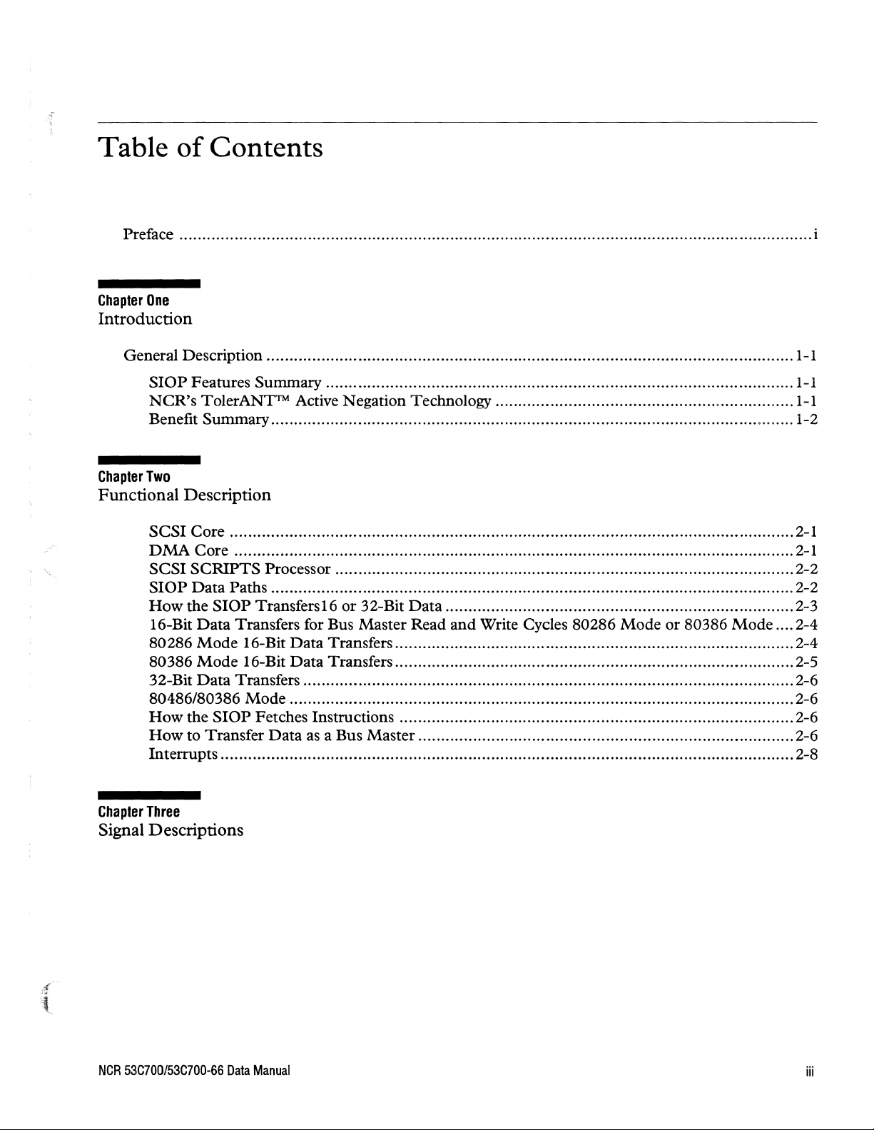
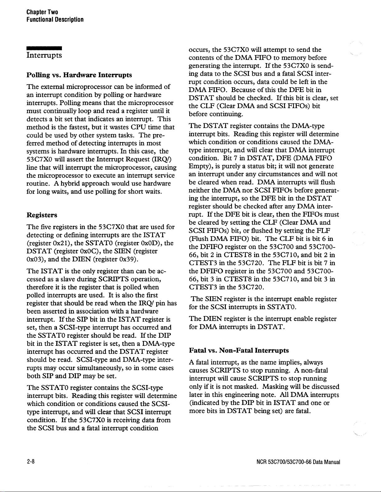
---------
DMACore
SCSI
FIFO
-----
--
--
SCSI
Data
Test
rl
11
SCSI
and
Reserved
DMA
Async
I
Sync
I
Registers
Registers
Registers
Control
Control
•
SCSI
I
I
I
I
---------
-
Control
SCSI
Sequences
~
ro--------
.on
cO·
c::
@
.....
I
.....
z
C")
::tI
U'I
Ct.)
C")
""-J
o
!i;2
U'I
Ct.)
C")
~
o
I
0)
0)
c::I
g
A
C
~.
PJ
3
-
C")
==-
:::1»
CI"CI
CI.
_
c::
m
n-
:::'c
CI=
=m
z
(")
jj
~
.....
~
n
.....
g
a.
C'>
c
s-
s:
~
s:::
e!...
DMA
FIFO
Host
Data
I/O
Control
-
SCRIPT
Host
Bus
Host
Processor
Control
Control
(
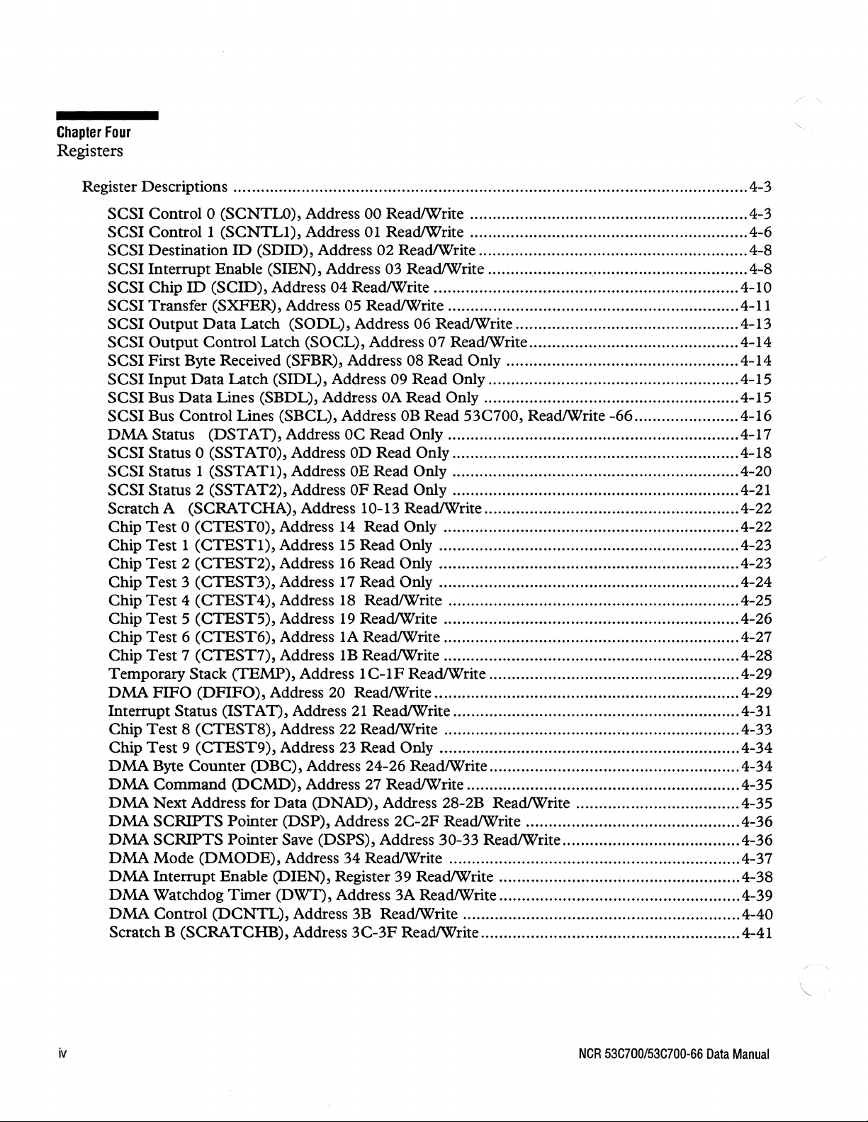
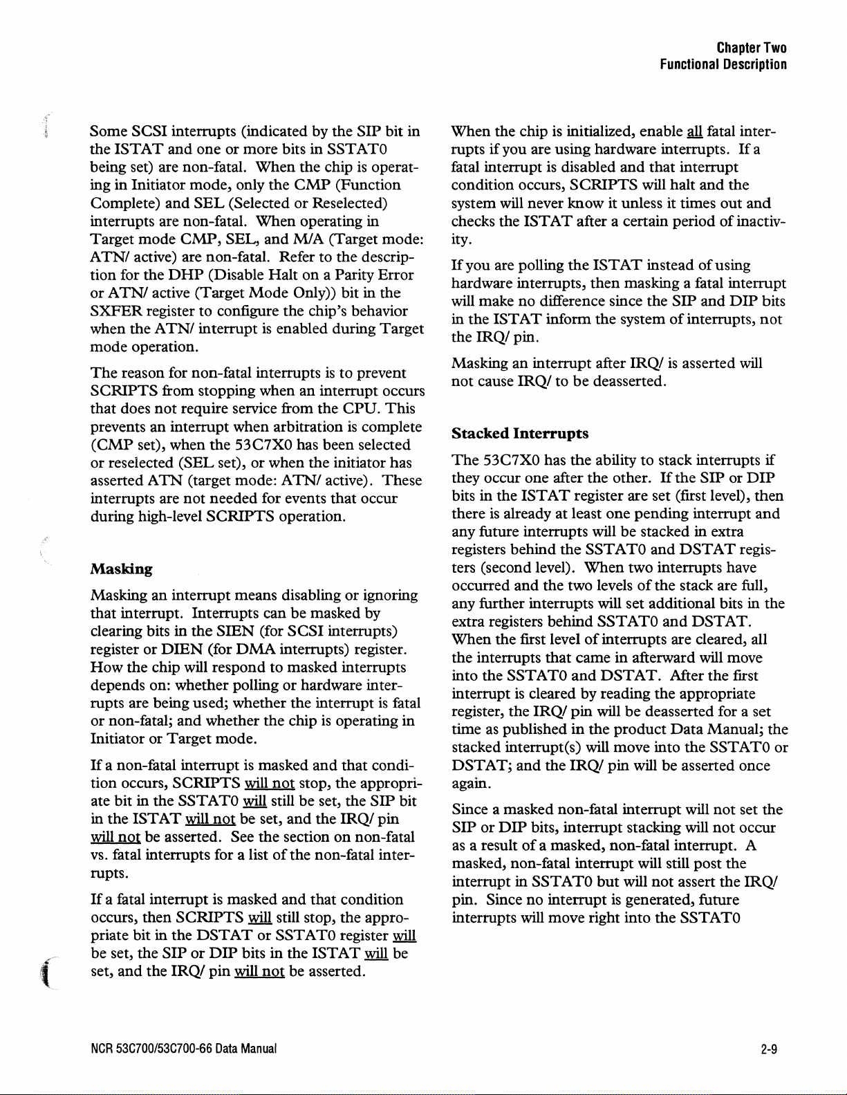
Page 13
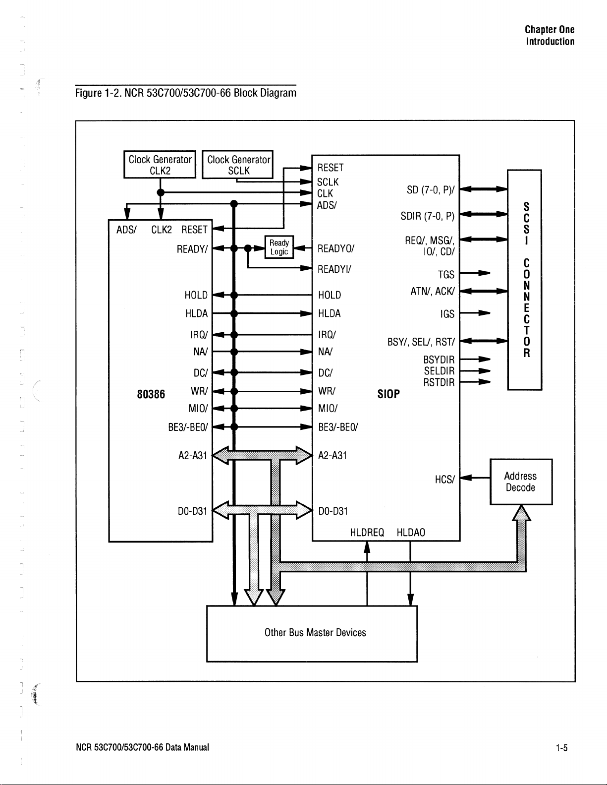
Figure
1-2.
ADSI
NCR
53C700/53C700-66
I
Clock
Generator
CLK2
t
CLK2
80386
RESET
READYI
HOLD
HLDA
BE3/-BEOI
Block
Diagram
II
Clock
Generato
SCLK
_ I
Ready
T
-1
-
IRQ! IRQ!
NN
DCI
-
..
WR/
MIOI MIOI
logic
..
- -
..
-
I---
-
-
-
..
..
..
RESET
SCLK
CLK
ADSI
READYOI
READY
HOLD
HLDA
NN
DCI
WRI
BE3/-BEOI
II
BSY/,
SlOP
SD
SDIR
REQ!,
ATN/,
SEU,
(7-0,
P)I
(7-0,
P)
MSG/,
101,
CDI
TGS
ACKI
IGS
RSTI
BSYDIR
SELDIR
RSTDIR
..
..
Chapter
Introduction
S
C
S
I
C
0
N
N
E
C
T
0
R
One
A2-A31
A2-A31
f4
DO-D31 DO-D31
~
.........
~
>
~
HLDREQ
Jf
Other
Bus
Master
Devices
HLDAO
r
HCSI
Address
Decode
J.
~
NCR
53C700/53C700-66
Data
Manual
1-5
Page 14

[
[
Page 15
pier
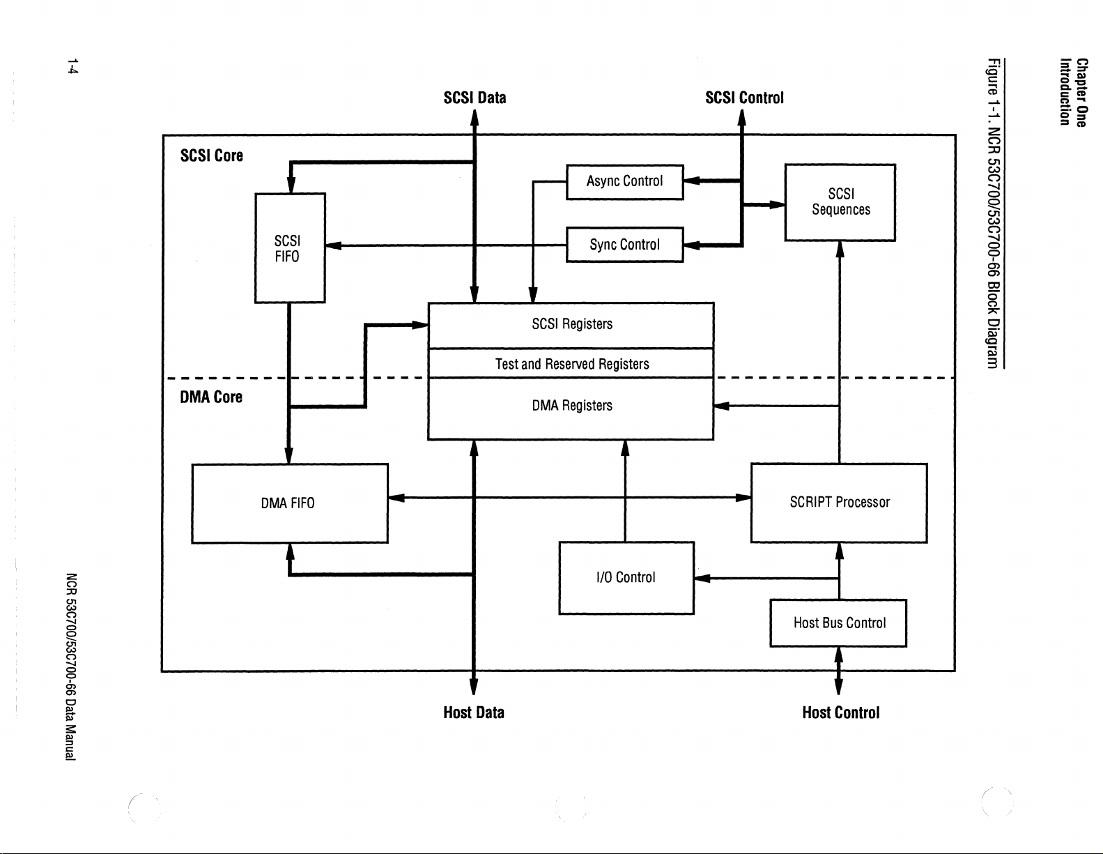
Functional Description
The
NCR
53C700
the first intelligent SCSI Host adapter on a chip.
A high-performance
32-bit bus master
integrated with a
accommodate the flexibility requirements
only
SCSI-I,
This flexibility
protocol performance problems that have plagued
both intelligent and non-intelligent adapter de-
(See the SCSI I/O Processor Block Diagrams
signs
in Figures
the same structure as the
features.
1-1
SCSI
I/O Processor (SlOP)
SCSI
core and an intelligent
DMA
SCSI
but
SCSI-2,
is
supported while solving the
and 1-2).
controller have been
SCRIPTS
and
The
53C700 plus added
Processor™ to
eventually SCSI-3.
53C700-66 contains
of
is
not
Chapter
Functional
ported.
selection and operate as
target.
physical connection to the board or the
Unlike previous generation devices, the
can be controlled by the
through a high level logical interface. Commands
controlling the
main Host memory. These commands instruct
the
for a disconnect, transfer information, change bus
phases and in general, implement all aspects
SCSI protocol.
The
SCSI
core may perform a self-
both
an initiator
The
53C700 can test the
SCRIPTS
SCSI core are fetched out
SCSI core to select, reselect, disconnect, wait
SCSI
pins for
SCSI bus.
SCSI core
Processor
Two
Description
and
a
of
the
of
the
J
,~
SCSI Core
The
SCSI core
tion to
nous transfer rate requirements.
offers synchronous transfers
asynchronous transfers
53C700-66 offers synchronous transfers
MB/s with asynchronous transfers
The
to
requirements or
The
high level control interface. Like first generation
SCSI devices, the
cessed as a register oriented device.
sample and/or assert any signal on the
can be used in error recovery and diagnostic
procedures. Loopback diagnostics are also sup-
SCSI-2 wide bus and enhanced synchro-
programmable SCSI interface makes it easy
"fine
tune"
SCSI core offers low level register access or a
is
designed to allow simple migra-
The
53C700
up
to 6.25 MB/s with
up
to 5 MB/s.
the system for specific mass storage
SCSI-2 requirements.
SlOP
SCSI
core can be ac-
The
up
to 5 MB/s.
The
SCSI bus
up
to 10
ability to
DMACore
The
DMA
attaches easily to the 80286, 80386,
and 80486 processors.
MHz
MHz
externally adapted to other system buses such
EISA, Micro Channel or attached through a "bus
gasket"
The
SlOP
automatically supports misaligned
As
with the 80386/80486, data bus enables are
provided for each byte lane. A 32-byte
allows the
or 32-bit) words to
bus interface providing memory transfer rates
to 47 MB/s for the 53C700
53C700-66.
core
is
a bus master
The
80386/80486 (the 53C700-66 supports 33
80386/80486) bus timings and may be
to a 680XO
supports 16 or 32-bit memory and
SlOP
device.
to support two, four, or eight (16
be
burst across the memory
DMA
53C700 supports 25
and
device that
80386SX,
as
DMA
62 MBlsec for the
transfers.
FIFO
up
(
NCR
53C700/53C700-66
Data
Manual
2-1
Page 16
Chapter
Functional
The
through
uninterrupted
Two
Description
DMA
the
core is tightly coupled
SCRIPTS
processor which supports
to
the
SCSI
scatter/gather memory operations.
core
A flexible arbitration scheme allows either daisychained
"ORed"
memory bus request imple-
or
mentations.
SCSI
SCRIPTSTM
Processor
new
bus device types (i.e. scanners, communication gateways, etc.),
the
SCSI-2/310gical bus defmitions without
sacrificing
SCSI
system
I/O
SCRIPTS
bus
in
use. Therefore, scripts for
implementation
the
scripts for
an
or
to
incorporate changes in
performance.
are independent
of
an
80386
80386SX
Micro
can
ofthe
be
identical
Channel
plementation.
CPU
an
im-
and
EISA
to
The
SCSI
SCRIPTS
processor
structions
that
to
allows
be
Algorithms written
the actions
executed
Complex
pendently
The
SCRIPTS
operation in
ofthe
from
SCSI
of
the
500
16
required for traditional intelligent
The
SCRIPTS
Processor
both
fetched from
in
SCSI
SCSI
and
or
32-bit system memory.
bus
sequences are executed inde-
Host
CPU.
Processor can begin a
ns.
This
is
a 2
DMA
and
Host
memory.
SCRIPTS
DMA
cores
compares
Host
MIPS
SCSI
can
and
SCSI
to
2-8
adapters.
control
Processor offers performance
in-
are
110
ms
and
customized algorithms. Design your own algorithms
Figure
to
2-1.
tune
SlOP
SCSI
Data
bus
performance,
Paths
to
adjust
SlOP
The
on
two things.
• Is
• Is
Figure 2-1 shows
the
To
determine
when
ing steps.
to
Data
data paths
data
SCSI
Paths
through
being moved
data being sent asynchronously
the
in
synchronously.
how
data
SCSI
bus
in
each
of
the
if
any
bytes remain in
the
chip halts any operation, take
SlOP
is
or
out
moved
are
dependent
of
the
to
four modes.
the
chip
or
from
data
the
or
path
follow-
2-2
Asynchronous
SCSI
Send
Asynchronous
SCSI
Receive
Synchronous
SCSI
Send
Synchronous
SCSI
Receive
NCR
53C700/53C700-66
Data
Manual
Page 17
Functional
Chapter
Description
Two
•
Asynchronous
Target
1.
Use the algorithm described in the
register description to determine
are left in the
2.
Read the
to determine
register.
in the
number
•
Synchronous
SST
SODL
of
Target
1. Use the algorithm described in the
register description to determine
are left in the
2. Read the SSTAT1 register and test bit 5 to
determine
register.
byte in the
to the number
3. Read the
determine
SODR
one byte in the
one to the number
•
Asynchronous
SST
register.
Target
1. Use the algorithm described in the
register description to determine
are left in the
2. Read the SSTAT1 register and test bit 7 to
determine
register.
byte in the
to the number
•
Synchronous
Target
SCSI
Send -Initiator
Operation
DFIFO
if
DMA
AT
if
If
bit 5 equals 1, then there
register and add one to the
bytes left.
FIFO.
1 register and examine bit 5
any bytes are left in the
SCSI
Send -Initiator
Operation
DFIFO
if
DMA
if
any bytes are left in the
Ifbit
SODL
AT
if
any bytes are remaining in the
FIFO.
5 equals
register, therefore, add one
of
bytes left.
1 register and test bit 6 to
Ifbit
SODR
SCSI
1,
then there
6 equals 1, then there
register, therefore, add
of
bytes left.
Receive -
Initiator
Operation
DFIFO
if
DMA
if
any bytes are left in the
If
bit 7 equals 1, then there
SIDL
SCSI
FIFO.
register, therefore,
of
bytes left.
Receive -
Initiator
Operation
and
any bytes
SODL
is
a byte
and
any bytes
SODL
is
one
any bytes
SIDL
is
one
add
one
is
and
and
2. Read the
(the binary representation
valid bytes in the SCSI FIFO) to determine
any bytes are left in the
How the
16
or 32-Bit Data
The
SlOP
transfer.
transferred are summarized below. These two bits
do not determine how
fetched.
register controls whether
loaded 16-bits per transfer or 32-bits per transfer.
Table
2-1.
BW16
o o
SST A T2
SlOP
can transfer data 16-bits or 32-bits per
The
two bits controlling how data
The
Scripts-16 bit in the
Block
Move
286M
Description
32-bit data transfers,
and expects
register
SCSI
Transfers
SCSI
SCSI
Transfer
80486/80386 signals
and
test bits 7-4
of
the number
FIFO.
SCRIPTS
DCNTL
SCRIPTS
Bit
Descriptions
SlOP
are
of
if
is
are
asserts
x 1 16-bit data transfers, (slave &
master mode)
expects
1
Key: BW16
In
bus master mode, the
data to
0 16-bit data transfers, (master mode
data transfers only)
and expects
= Bus Width 16-bit in the
DMODE
286M
X
an
= 80286 Mode bit in the
=
Don't
odd-byte boundary address.
80286 signals
register
SlOP
80386 signals
register
Care
SlOP
optimizes moving
asserts and
SlOP
asserts
DMODE
1.
Use the algorithm described in the
register description to determine
are left in the
NCR
53C700/53C700-66
DMA
Data
FIFO.
Manual
DFIFO
if
any bytes
2-3
Page 18
Chapter
Functional
Two
Description
16-Bit
Master Read
80286
The
tion
instruction.
register.
first Block Move operation
DlS-D8,
transfer
DPO.
complete a Block Move instruction,
will
DPO.
Data
Mode
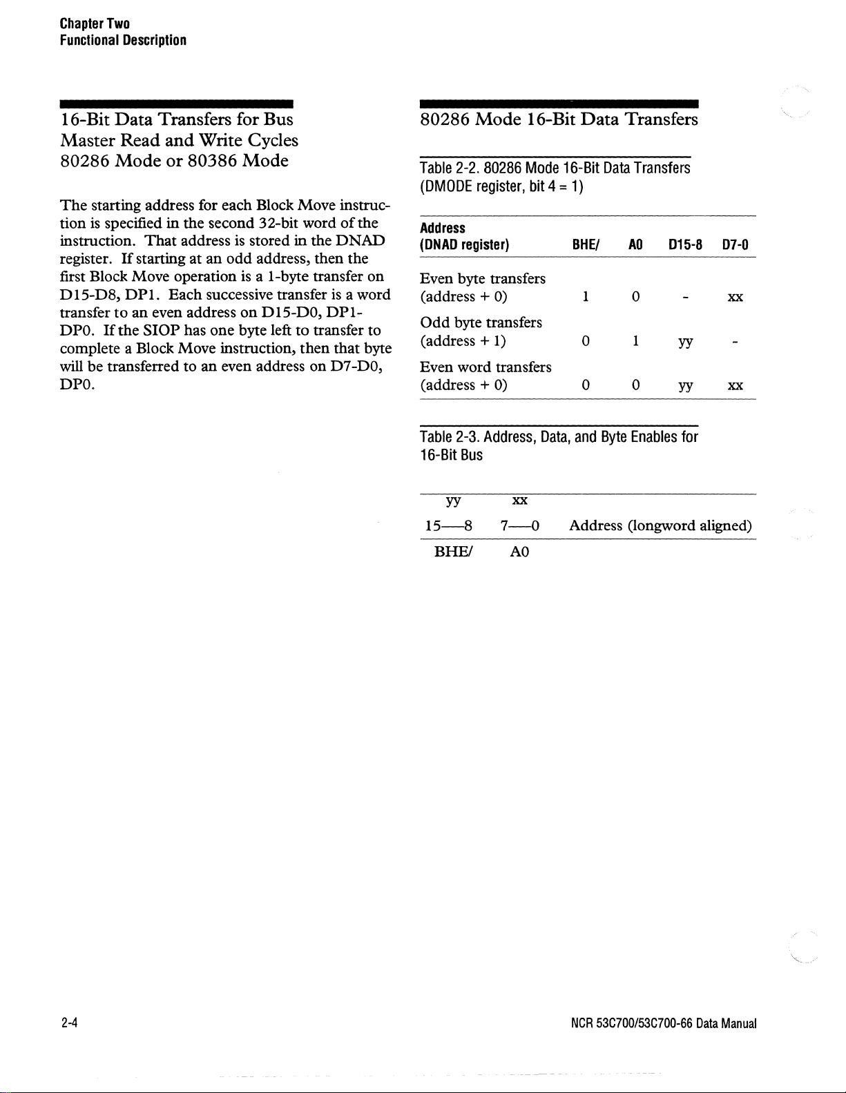
starting address for each Block Move instruc-
is
specified
to
If
be
transferred
Transfers for Bus
and
Write Cycles
or
80386
in
the
second 32-bit word
That
address is stored
If
starting
DPl.
an
the
SlOP
at
an
Each
successive transfer
even address
has
to
an
Mode
odd
address,
is
a I-byte transfer
on
DIS-DO,
one
byte left
even address
in
the
then
to
transfer to
then
on
of
the
DNAD
the
is
a word
DPl-
that
byte
D7-DO,
on
80286
Table
(DMODE
Address
(DNAD
Even byte transfers
(address
Odd
(address
Even word transfers
(address
Table
16-Bit
Mode
2-2.
80286
register,
register)
+ 0)
byte transfers
+ 1) 0
+ 0)
2-3.
Address,
Bus
yy
xx
16-Bit
Mode
bit
Data,
16-Bit
4 =
Data
Data
1)
BHEI
1
0 0
and
Byte
Transfers
Transfers
015-8
AO
0
1
Enables
yy
yy
for
D7-0
xx
xx
15-8
BHEI
7--0
AO
Address (longword aligned)
2-4
NCR
53C700/53C700-66
Data
Manual
Page 19
Functional
Chapter
Two
Description
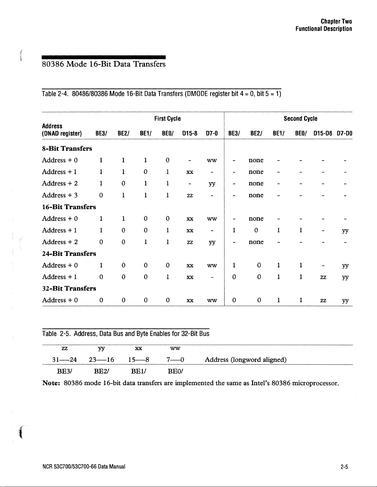
80386
Table
Address
(ONAO
8-Bit
Address + 0
Address + 1
Address + 2
Address + 3 0
16-Bit
Address + 0
Address + 1
/
Address + 2 0 0
Mode
2-4.
80486/80386
register)
Transfers
Transfers
16-Bit
Data
Mode
BE31
1
1 1
1
1 1 0 0
1
Transfers
16-Bit
BE2/
1 1
0
1
0 0
Data
BEll
0
1 1
1 1
1 1
Transfers
First
BEOI
0
1 xx
Cycle
015-8 07-0
(DMODE
ww
yy
register
BE31
zz
xx
1 xx 1 0
zz
ww
yy
bit
4 =
0,
bit
BE2/
none
none
none
none
none
none
5 =
1)
BEll
Second
BEOI
1 1
Cycle
015-08 07-00
yy
24-Bit
Address + 0
Address + 1 0 0 0
32-Bit
Address + 0 0
Table
Note:
Transfers
Transfers
2-5.
zz
31-24
BE31
80386
Address,
23-16
BE2I
mode
1
Data
yy
0
0 0 0
Bus
and
Byte
xx
15-8
BEll
16-bit data transfers are implemented the same as Intel's
0 0
1 xx
Enables
7-0
for
ww
BEOI
xx
xx
32-Bit
ww
ww
1 0
0 0
0 0 1
Bus
Address (longword aligned)
80386
1 1 yy
1 1
1
microprocessor.
zz
zz
yy
yy
('
NCR
53C700/53C700-66
Data
Manual
2-5
Page 20
Chapter
Functional
32-Bit
The
tion
instruction stored in
If
the
first Block
transfer
and
transfer will
BE3/-BEOI all driven active.
If
complete a Block Move instruction,
bytes will be transferred
with
If
complete a Block Move instruction,
will
driven active.
If
a Block Move instruction, those bytes
transferred
BEll,
80486/80386
Table
Two
Description
Data
starting address for each Block Move instruc-
is
specified in
bit 0 = 1,
DBC
on
BEll
the
SlOP
BEll
the
SlOP
be
transferred
the
SlOP
and
Transfers
the
second 32-bit word
the
DNAD
and
the
Byte
Counter
register
Move
D3I-D8,
all driven active.
and
BEOI driven active.
is
greater
operation involves a 3-byte
DP3-DPI
occur
on
D31-DO, DP3-DPO with
has two-bytes
BEOI driven active.
has one-byte
on
has three-bytes
on
D23-DO, DP2-DPO with BE2I,
to
on
to
D7-DO, DPO with BEOI
register.
Value stored
than
three,
with BE3/, BE2I,
Each
successive
transfer in order
DIS-DO,
transfer in
to
transfer to complete
then
then
DPI-DPO
order
then
will
Mode
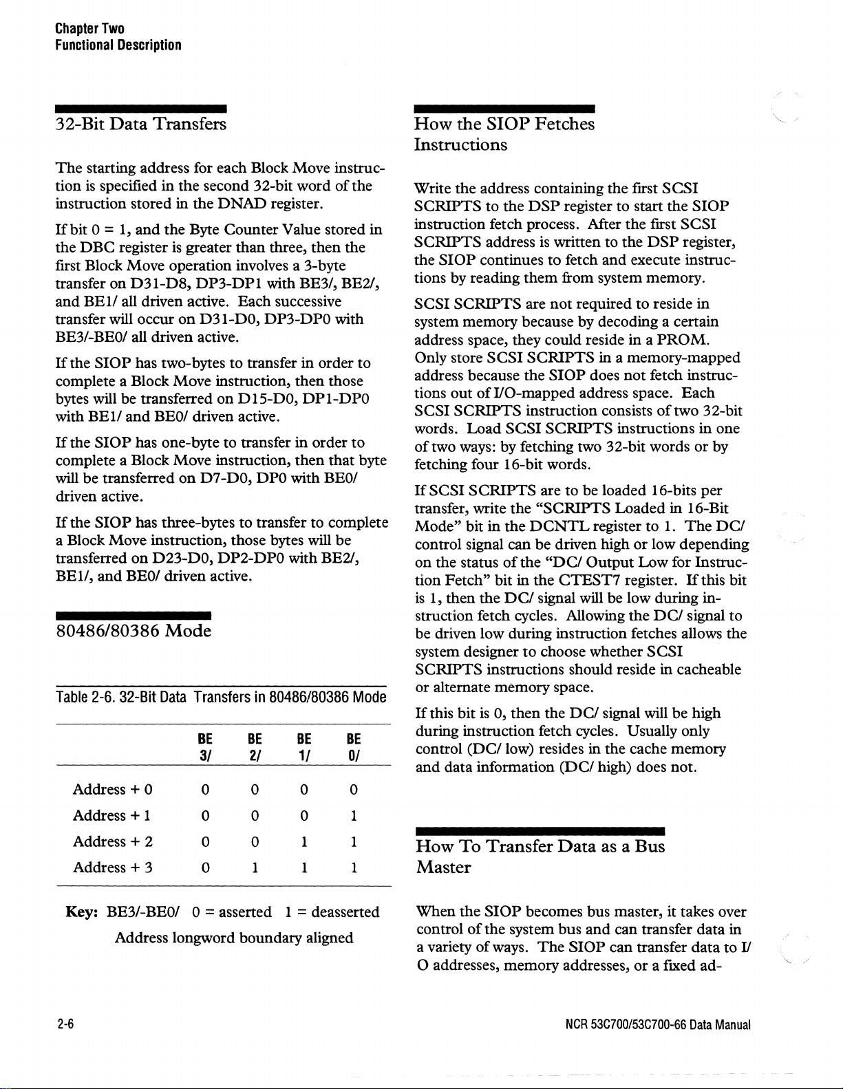
2-6.
32-Bit
Data
Transfers
BE
3/
Address + 0 0 0 0 0
in
80486/80386
BE
2/
BE BE
1/
ofthe
the
to
those
to
that
be
Mode
0/
in
byte
How
the
SlOP
Fetches
Instructions
Write
the
address containing
SCRIPTS
instruction fetch process.
SCRIPTS
the
SlOP
tions by reading
SCSI
system
address space, they could reside
Only store
address because
tions
SCSI
words.
of
two ways: by fetching two 32-bit words
fetching four 16-bit words.
If
SCSI
transfer, write
Mode"
control signal can
on
the
tion
is
I,
struction fetch cycles. Allowing
be
driven low during instruction fetches allows the
system designer
SCRIPTS
or
alternate
If
this
during instruction fetch cycles.
control
and
to
address
continues
SCRIPTS
memory
SCSI
out
of
1I0-mapped
SCRIPTS
Load
SCRIPTS
bit
in
status
Fetch"
then
the
instructions should reside in cacheable
bit
is
0,
(DCI
data
information
the
DSP
register to start
is
written to
to
fetch
them
from system memory.
are
not
because by decoding a certain
SCRIPTS
the
SlOP
instruction consists
SCSI
SCRIPTS
are to
the
"SCRIPTS
the
DCNTL
be
driven high
of
the
"DCI
bit
in
the
CTEST7
DC!
signal will be low
to
choose whether
memory
then
low) resides in
space.
the DC! signal will
(DCI
the
first
SCSI
the
Mter
the
first
SCSI
the
DSP
register,
and
execute instruc-
required
does
address space.
be
register
Output
to
reside
in a PROM.
in a memory-mapped
not
fetch instruc-
Each
of
two 32-bit
instructions
loaded 16-bits
Loaded
register.
Usually only
the
high) does not.
in 16-Bit
to
1.
The
or
low depending
Low
for Instruc-
Ifthis
during
the
DCI
signal
SCSI
be
cache
memory
SlOP
in
or
high
in
by
per
in-
one
DCI
bit
to
\
""'-.
,/
Address + I 0 0
Address
Address
Key:
2-6
+ 2 0
+ 3
BE3/-BEOI
Address longword boundary aligned
0
0=
asserted 1 = deasserted
0
0
I I 1
1 I
1
How
To
Transfer
Master
When
control
a variety
the
of
SlOP
the
of
o addresses,
Data
becomes bus master, it takes over
system bus
ways.
The
memory
as a Bus
and
can
SlOP
can
transfer
addresses,
NCR
53C700/53C700-66
or a fIXed
transfer
data
data
ad-
Data
in
to II
Manual
Page 21
Functional
Chapter
Description
Two
dress.
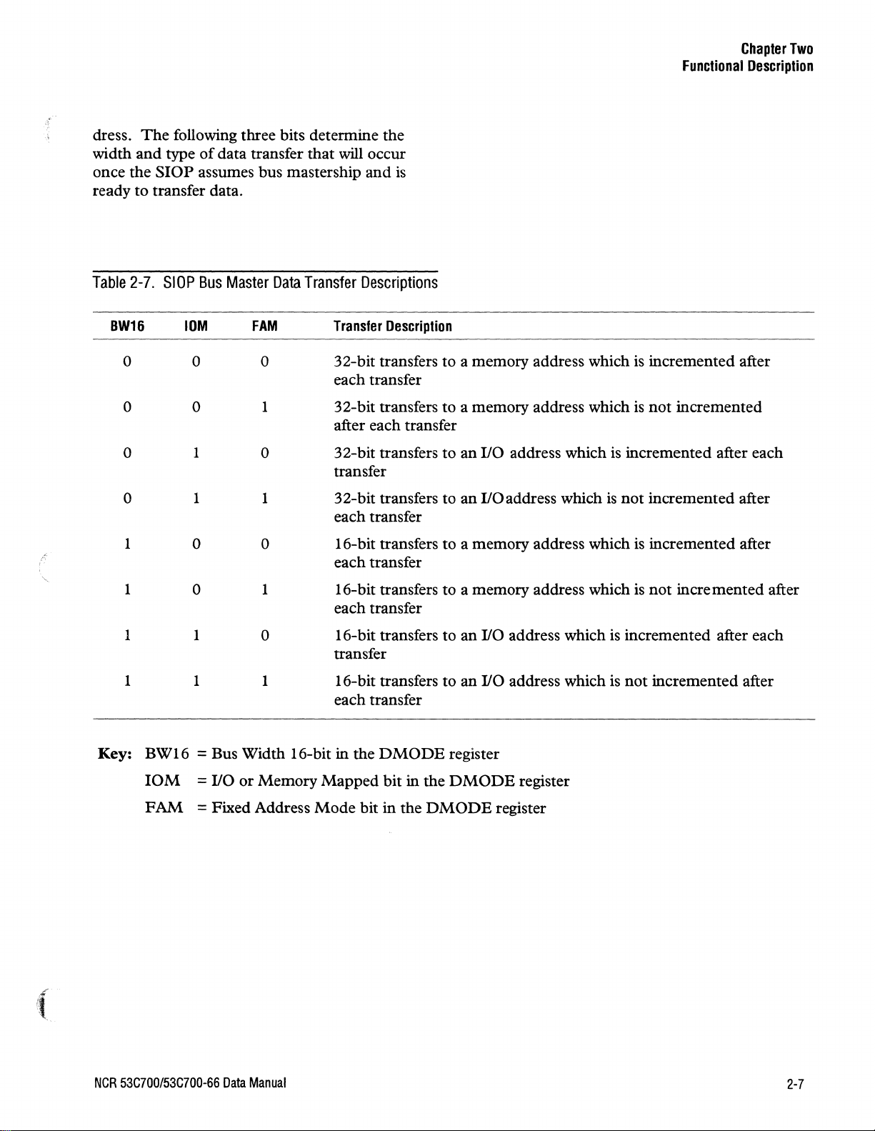
width and type
once the
The
following three bits determine the
of
data transfer that will occur
SlOP
assumes bus mastership and
is
ready to transfer data.
Table
2-7.
SlOP
Bus
BW16
0 0
Master
10M
Data
FAM
0
Transfer
Descriptions
Transfer
Description
32-bit transfers to a memory address which
is
incremented after
each transfer
0 0
1
32-bit transfers to a memory address which
is
not incremented
after each transfer
0
1
0
32-bit transfers to an
110 address which
is
incremented after each
transfer
0 1
1
32-bit transfers to an
110 address which
is
not
incremented after
each transfer
1
0
0
16-bit transfers to a memory address which
is
incremented after
each transfer
"-
I
0 1 16-bit transfers to a memory address which
is
not incremented after
each transfer
(
1 1
1 1
Key: BW16
10M = 110
FAM
0
16-bit transfers to an
transfer
1
16-bit transfers to an
each transfer
= Bus Width 16-bit in the
or Memory Mapped bit in the
= Fixed Address
Mode
bit in the
DMODE
DMODE
110
110
register
DMODE
register
address which
address which
register
is
incremented after each
is
not
incremented after
NCR
53C700/53C700-66
Data
Manual
2-7
Page 22
Chapter
Functional
Two
Description
Interrupts
Polling
The
an interrupt condition by polling
interrupts. Polling means that the microprocessor
must continually loop and read a register until it
detects a bit set that indicates an interrupt. This
method
could be used by other system tasks.
ferred method
systems
53C7XO
line that will interrupt the microprocessor, causing
the microprocessor to execute an interrupt service
routine. A hybrid approach would use hardware
for long waits, and use polling for short waits.
Registers
The
detecting or defining interrupts are the
(register
DSTAT
Ox03), and the
The
cessed
therefore it
polled interrupts are used.
register that should be read when the IRQ! pin has
been asserted in association with a hardware
interrupt.
set, then a SCSI-type interrupt has occurred and
the
bit in the 1ST
interrupt has occurred
should be read.
rupts may occur simultaneously,
both
The
interrupt bits. Reading this register will determine
which condition or conditions caused the
type interrupt,
condition.
the
vs.
Hardware
Interrupts
external microprocessor can be informed
or
hardware
is
the fastest,
of
is
hardware interrupts.
will
assert the Interrupt Request (IRQ!)
five
registers in the 53C7XO that are used for
but
it wastes
CPU
The
time that
pre-
detecting interrupts in most
In
this case, the
1ST A T
Ox21), the SSTATO (register
(register
1ST
AT
as
a slave during SCRIPTS operation,
If
OxOC),
DIEN
is
the only register than can be ac-
is
the register
the SIP bit in the
the
SIEN
(register
that
It
Ox39).
is
polled when
is
also the first
ISTAT
SSTATO register should be read.
AT
SIP
and
register
SCSI-type
DIP
may be set.
is
set, then a DMA-type
and
the
DST
and
DMA-type inter-
OxOD),
(register
register
If
the
A T register
so
in some cases
SSTATO register contains the SCSI-type
SCSI-
and
will clear that SCSI interrupt
If
the 53C7XO
is
receiving data from
SCSI bus and a fatal interrupt condition
of
the
is
DIP
occurs, the 53C7XO will attempt to send the
of
the
contents
DMA
generating the interrupt.
ing data to the
rupt
condition occurs, data could be left in the
DMA
DSTA
the
FIFO.
T should be checked.
CLF
SCSI bus and a fatal SCSI inter-
Because
(Clear
DMA
FIFO
to memory before
If
the 53C7XO
of
this the
If
this bit
DFE
is
bit in
is
and SCSI FIFOs) bit
send-
clear, set
before continuing.
The
DSTAT
register contains the DMA-type
interrupt bits. Reading this register will determine
or
which condition
type interrupt,
condition. Bit 7 in
Empty), is purely a status bit; it
an interrupt under any circumstances
be cleared when read.
neither the
DMA
ing the interrupt, so the
register should be checked after any
If
the
rupt.
DFE
be cleared by setting the
SCSI
FIFOs) bit, or flushed
(Flush
the
66, bit 2 in
CTEST3
the
66, bit 3 in
CTEST3
The
for the
The
for
Fatal
DMA
DFIFO
register
CTEST8
in the 53C720.
DFIFO
register in the 53C700 and 53C700-
CTEST8
in the 53C720.
SIEN
register
SCSI interrupts in SSTATO.
DIEN
DMA
register
interrupts in
vs.
Non-Fatal
A fatal interrupt,
causes
interrupt
only
SCRIPTS to stop running. A non-fatal
will
if
it
is
not
later in this engineering note. All
(indicated by the
more bits in
DSTAT
conditions caused the DMA-
and
will
DSTAT,
DMA
nor
SCSI
bit
is
FIFO) bit.
on
the 53C700
clear that
DFE
clear,
CLF
The
DMA
DFE
will
interrupts
FIFOs
bit in the
then
the FIFOs must
(Clear
by
setting the
CLF
interrupt
(DMA
not
and
FIFO
generate
will
not
will
flush
before generat-
DST
AT
DMA
DMA
inter-
and
FLF
bit
is
bit 6 in
and
53C700-
in the 53C710, and bit 2 in
The
FLF
bit
is
bit 7 in
in the 53C71 0, and bit 3 in
is
the interrupt enable register
is
the interrupt enable register
DSTAT.
Interrupts
as
the name implies, always
cause
SCRIPTS
to
stop running
masked. Masking will be discussed
DIP
bit in
DMA
ISTA T and
interrupts
one or
being set) are fatal.
2-8
NCR
53C700/53C700-66
Data
Manual
Page 23
.f
I
~
(
Some
the 1ST
being set) are non-fatal. When the chip
ing in Initiator mode, only the
SCSI
interrupts (indicated by the SIP bit in
AT
and one or more bits in SSTATO
Complete) and
SEL
(Selected
CMP
(Function
or
Reselected)
is
operat-
interrupts are non-fatal. When operating in
Target mode
CMP,
SEL, and
MIA
(Target mode:
ATN! active) are non-fatal. Refer to the descrip-
DHP
tion for the
or
ATN! active (Target
SXFER
register to configure the chip's behavior
(Disable Halt
Mode
when the ATN! interrupt
on
a Parity Error
Only)) bit in the
is
enabled during Target
mode operation.
The
reason for non-fatal interrupts
SCRIPTS
that does
prevents
(CMP
or
res elected (SEL set),
asserted A
from stopping when an interrupt occurs
not
require service from the
an
interrupt when arbitration
set), when the 53C7XO has been selected
or
TN
(target mode: A
when the initiator has
is
to prevent
CPU.
is
TN!
active). These
This
complete
interrupts are not needed for events that occur
during high-level
SCRIPTS
operation.
Masking
Masking an interrupt means disabling
or
ignoring
that interrupt. Interrupts can be masked by
the
clearing bits in
or
register
How
DIEN
the chip will respond to masked interrupts
SIEN
(for
depends on: whether polling
rupts are being used; whether the interrupt
or
non-fatal; and whether the chip
(for
DMA
SCSI
interrupts)
interrupts) register.
or
hardware inter-
is
fatal
is
operating in
Initiator or Target mode.
If
a non-fatal interrupt
tion occurs,
ate bit in the
in the 1ST
will
not
SCRIPTS
SST A TO
AT
will
be asserted. See the section
vs. fatal interrupts for a list
is
masked
will
not
stop, the appropri-
will still be set, the
not
be set,
and
of
the non-fatal inter-
and
that condi-
the IRQ!
on
non-fatal
SIP
pin
bit
rupts.
If
a fatal interrupt
occurs, then
priate bit in the
be set, the
and
set,
SIP
the IRQ!
is
masked and that condition
SCRIPTS
DST
AT
or
DIP
pin
will
l£ill.
still stop, the appro-
or
SST A TO
bits in the
not
ISTAT
be asserted.
register
will be
M11.
Chapter
Functional
When the chip
if
rupts
you are using hardware interrupts.
fatal interrupt
condition occurs,
is
initialized, enable all fatal inter-
is
disabled
SCRIPTS
and
that interrupt
will halt and the
system will never know it unless it times out
checks the 1ST A T after a certain period
of
Two
Description
If
a
and
inactiv-
ity.
If
you are polling
the
ISTAT
instead
of
using
hardware interrupts, then masking a fatal interrupt
SIP
and
DIP
will make no difference since the
AT
in the 1ST
inform the system
of
interrupts,
bits
not
the IRQ! pin.
Masking an interrupt after IRQ!
not
cause IRQ! to be deasserted.
Stacked
The
Interrupts
53C7XO has the ability to stack interrupts
they occur one after the other.
bits in the 1ST
is
there
already at least one pending interrupt
any future interrupts will
registers behind
AT
register are set (first level), then
be
the
SSTATO
is
asserted
If
the
SIP
or
stacked in extra
and
DSTAT
will
if
DIP
and
registers (second level). When two interrupts have
occurred
the two levels
of
the stack are full,
and
any further interrupts will set additional bits in the
extra registers behind
When the first level
of
SSTATO
interrupts are cleared, all
and
DSTAT.
the interrupts that came in afterward will move
into the
interrupt
SSTATO
is
cleared by reading the appropriate
register, the IRQ!
as
time
published
stacked interrupt(s) will move into the
DSTAT;
and
and
DSTAT.
pin
will
in
the product
be
After the first
de asserted for a set
Data
Manual; the
SSTATO
the IRQ! pin will be asserted once
or
again.
not
not
set the
occur
Since a masked non-fatal interrupt will
or
DIP
SIP
as
a result
bits, interrupt stacking will
of
a masked, non-fatal interrupt. A
masked, non-fatal interrupt will still post the
interrupt in
pin. Since
SSTATO
no
interrupt
interrupts will move right into the
but
will
not
is
generated, future
assert the IRQ!
SST A TO
NCR
53C700/53C700-66
Data
Manual
2-9
Page 24
Chapter
Functional
Two
Description
instead
of
being stacked behind another interrupt.
When another condition occurs that generates an
interrupt, the bit corresponding
masked non-fatal interrupt
A related situation to interrupt stacking
two interrupts occur simultaneously.
stacking does not occur until the SIP or
to
will
still be set.
the earlier
is
when
Since
DIP
bits
are set, there is a small timing window in which
multiple interrupts can occur
stacked. These could be multiple
(SIP set), multiple
multiple
SIP and
As
attempt
interrupt.
(Clear
(Flush
SCSI
DIP
previously mentioned,
to
flush the
It
DMA
DMA
occurs and the
not set. This
rupts will
clear
will
not
of
data. These 'locked out' SCSI interrupts
be posted as soon
DMA
and multiple
set).
FIFOs
is
important to set either the
and SCSI FIFOs) bit or the
FIFO) bit
DFE
(DMA
is
because any future SCSI inter-
be
posted until the
as
but
will
not
be
SCSI interrupts
interrupts (DIP set),
DMA
DMA
interrupts (both
interrupts will
before generating the
CLF
FLF
if
a
DMA
FIFO
the
DMA
DMA
interrupt
Empty) bit
FIFO
FIFO
is
or
not
is
is
empty.
Halting
When an interrupt occurs, the 53C7XO
attempt
•
•
in
an
to
halt in an orderly fashion.
If
in the middle
Orderly
Fashion
will
of
an instruction fetch, the
fetch will be completed, except in the case
Bus Fault
will
next instruction since it
current
If
the
not
DMA
or
Watchdog Timeout. Execution
begin,
Script
but
the
is
fetched.
direction
DSP
will point to the
is
updated when the
is
a write to memory
of
and
a SCSI interrupt occurs, the 53C7XO will
to
attempt
flush the
before halting.
DMA
Under
FIFO
to memory
any other circumstances
only the current cycle will be completed before
halting, so the
checked to see
DSTAT
if
any data remains in the
should be
DMA
DFE
bit in
FIFO.
•
The
53C7XO will attempt to clean
outstanding synchronous offset before halting.
•
In
the case
of
Transfer Control Instructions,
once instruction execution begins it will
continue to completion before halting.
•
If
the instruction
<phase>, the
is a JUMP/CAlL
DSP
will
be updated to the
transfer address before halting.
• All other instructions may halt before completion.
Sample
The
routine for the
polling
pin
1. Read
2.
Interrupt
following
is
used, or should be called when the
is
asserted
Service
is
a sample
53C7XO.
if
hardware interrupts are used.
Routine
of
an interrupt service
It
can be repeated
ISTAT
If
only the SIP bit
the
SCSI interrupt condition and get the SCSI
interrupt status.
which
SCSI
is
set, read SSTATO to clear
The
bits in the
SSTA
interrupt(s) occurred and determine what action is required to service the
interrupt(s) .
If
3.
only the
DIP
bit
is
set, read the
DSTAT
clear the interrupt condition and get the
interrupt status.
tell which
a
determine what action
the interrupt(s).
If
both
4.
SSTATO
DMA
the SIP
and
SCSI and
The
bits in the
interrupt(s) occurred
is
required to service
and
DIP
bits are set, read
DSTAT
DMA
as a word
interrupt condition
DSTAT
to
the interrupt status. Ifusing 8-bit reads
SSTATO and
interrupts, insert 10
DSTAT
CLKs on the 53C700 and
registers to clear
53C700-66, and 12 CLKs on the 53C710
between the consecutive reads to ensure that
the interrupts clear properly. Both the
and
DMA
handled before leaving the
interrupt conditions should be
ISR.
It
up
any
WHEN
if
mQl
TO
DMA
and
clear the
and
ofthe
SCSI
is
recom-
tell
to
will
get
• SCSI REQI
will
be completed before halting.
2-10
ACK
handshakes that have begun
NCR
53C700/53C700-66
Data
Manual
Page 25
Chapter
Functional
Two
Description
mended that the
before the
DMA
interrupt condition could influence how
the SCSI interrupt
DMA
SCSI
interrupt because a serious
interrupt be serviced
is
acted upon.
5. When using polled interrupts, go back to step
1 before leaving the interrupt service routine,
in case any stacked interrupts moved in when
the
first interrupt was cleared. When using
pin
hardware interrupts, the IRQ!
if
asserted again
there are any stacked inter-
will be
rupts. This should cause the system to reenter the interrupt service routine.
NCR
53C700/53C700-66
Data
Manual
2-11
Page 26

L
I
L
I
L
L
[
'~
Page 27
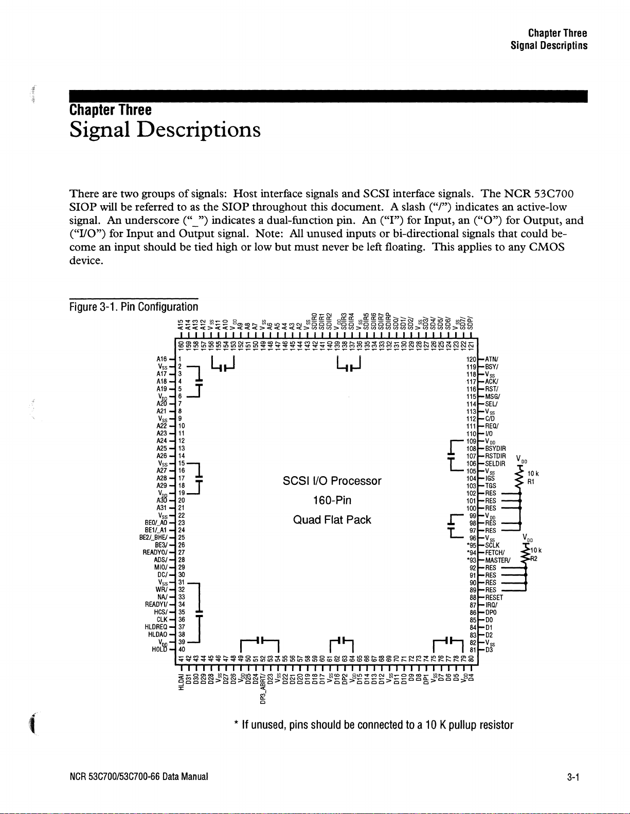
Chapter
Signal
Three
Descriptins
apler
Three
Signal Descriptions
There
SlOP
signal.
("lIO") for
come
device.
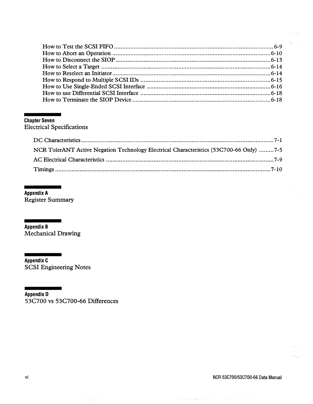
Figure
are two groups
will be referred to as the
of
signals:
Host
SlOP
throughout this document. A slash
An underscore ("_") indicates a dual-function pin. An ("I") for Input,
Input
an
input should be tied high
3-1.
Pin
and
Output
Configuration
A16
1
Vss
A17
~J.
A18
A19
iJ
:~8
7
A21
8
9
Vss
A22
10
A23
11
A24
12
A25
13
A26
14
Vss
15!
A27
16
A28
17
J
18
A29
19
:~8
20
A31
21
22
Vss
BEOLAD
BE1LA1
BE2LBHEI
READYOI
READYI/
HLDREQ
23
24
25
26
BE3/
27
28
ADSI
MIOI
29
DCI
30
Vss
WR!
32
NAt
33
34
"1
HCSI
35
CLK
36J
37
HLDAO
38
V
39
HOL'IS
40
;~~~~~~~~g~~~~~~~~m~~~~~~m~mm~~~~~~re~~~~
signal. Note:
or
low
L..J
r"-'
interface signals
All
unused
but
must never be left floating.
SCSI
1/0
Processor
160-Pin
Quad Flat Pack
r'"
and
SCSI
inputs
or
~.J
interface signals.
("I")
The
indicates an active-low
an
("0")
bi-directional signals
This
applies
ATNI
BSYI
Vss
ACK/
RSTI
Msal
SEU
Vss
C/O
REat
I/O
Voo
BSYOIR
RSTDIR
SELDIR
Vss
las
Tas
RES
RES
RES
Voo
RES
RES
Vss
FETCH!
S~K~
MASTER!
RES
RES
RES
RES
RESET
IRat
OPO
DO
D1
,,--,
02
Vss
03
NCR
53C700
for Output,
that
could be-
to
any
CMOS
Voo
10k
R1
Voo
10
and
k
(
NCR
53C700/53C700-66
Data
Manual
* If
unused,
pins
should
be
connected
to
a 10K
pullup
resistor
3-1
Page 28
Chapter
Signal
Descriptions
Three
3·2
NCR
53C700/53C700·66
Data
Manual
Page 29
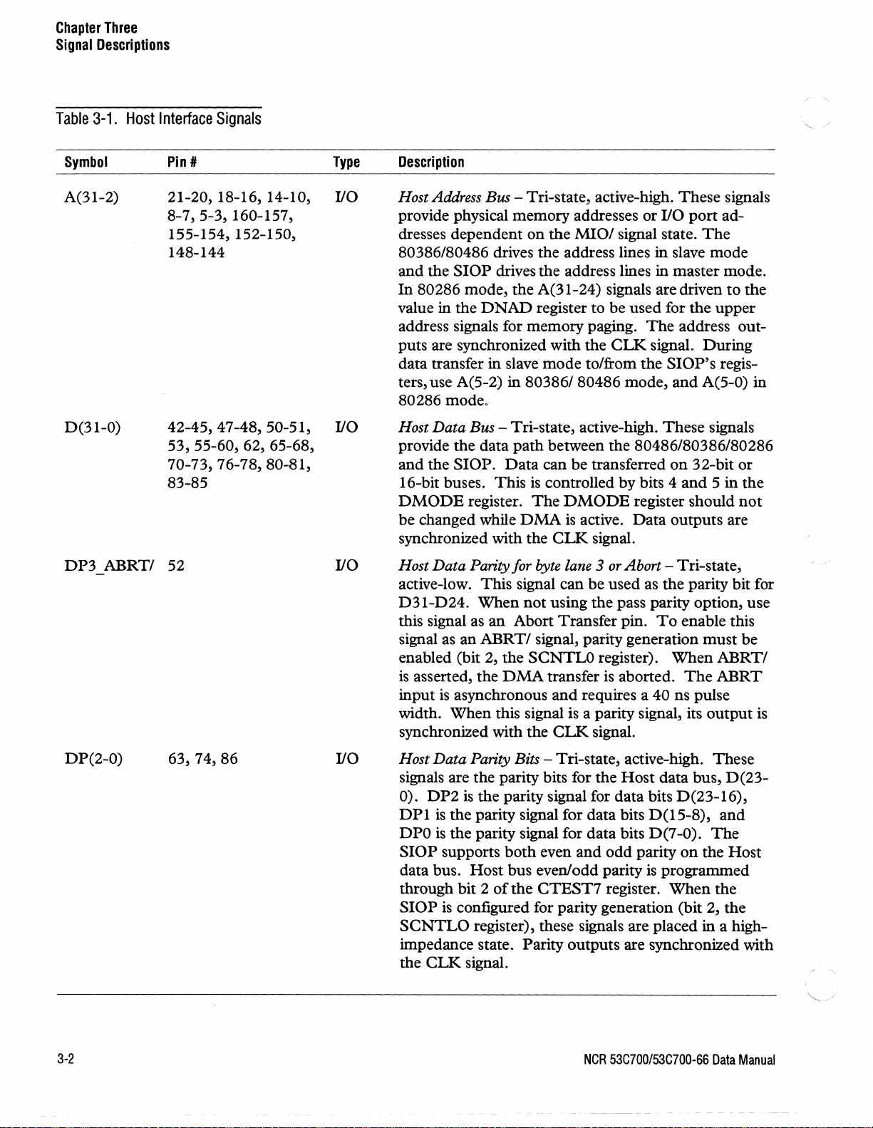
Table
Symbol
3-1.
Host
Interface
Pin
II
Signals
(Continued)
Type
Description
Chapter
Signal
Three
Descriptins
BE31
26
I/O
Byte Enable,
BE3/
- Tri-state, active-low. This signal
enables data transfer in the D(31-24) data byte lane.
It
is
driven by the
mode and driven by the
In
286 mode, this signal
pulled high. Bit 4
whether the chip operates in 286 mode
mode.
The
Host
output
when the
SlOP
is
not
of
the
DMODE
is
synchronized with the eLK
SlOP
is
in slave
during a
defmed
DMA
and
register determines
or
386/486
transfer.
should be
signal.
BE21
BHEI 25 I/O
Byte Enable,
active-low.
BE2/
or Byte High Enable/ - Tri-state,
In
386/486 mode, this signal enables data
transfers on the D(23-16) data byte lane.
In
286
mode, it distinguishes between 8-bit and 16-bit data
of
the
transfers. Bit 4
DMODE
whether the chip operates in 286
output
BEll
Al
.
.f
24 I/O
Byte Enable,
low.
is
synchronized with
BEI/
or Address,
In
386/486 mode, this signal enables data trans-
fer in the D(15-8) data byte lane.
pin
is
active-high, address line
Al
of
connected to
Bit 4
of
the
DMODE
chip operates in 286
the 80286.
register determines whether the
or
386/486 mode.
register determines
or
386 mode.
the
eLK signal.
Al
- Tri-state, active-
In
286 mode, this
AI,
and
should be
The
The
output
is
synchronized with the eLK signal.
(
BEOI
AO
WRI
NCR
53C700/53C700-66
23 I/O
32 I/O
Data
Manual
Byte Enable, BEO/ or Address, AO - Tri-state, active-
In
low.
the
tri-state, active-high
connected to the
DMODE
operating in 286
nized with the
Write
of
slave mode, high
from the chip. When the
high
the system bus.
386 mode, this signal enables data transfers
D(7
-0) data byte lane.
and
AO
pin
register determines whether
or
386 mode.
In
286 mode, this signal
used as address line
of
the 286. Bit 4
the
The
output
eLK signal.
or
Read/-
bus cycle being performed. When the
is
a write to the system bus
Tri-state. This signal defines the type
is
a write to the chip
SlOP
The
output
is
synchronized with the
and
is
in master mode,
and
low
AO,
ofthe
chip
is
is
synchro-
SlOP
is
low
is
a read
is
a read from
eLK signal.
on
is
in
3-3
Page 30
Chapter
Signal
Descriptions
Three
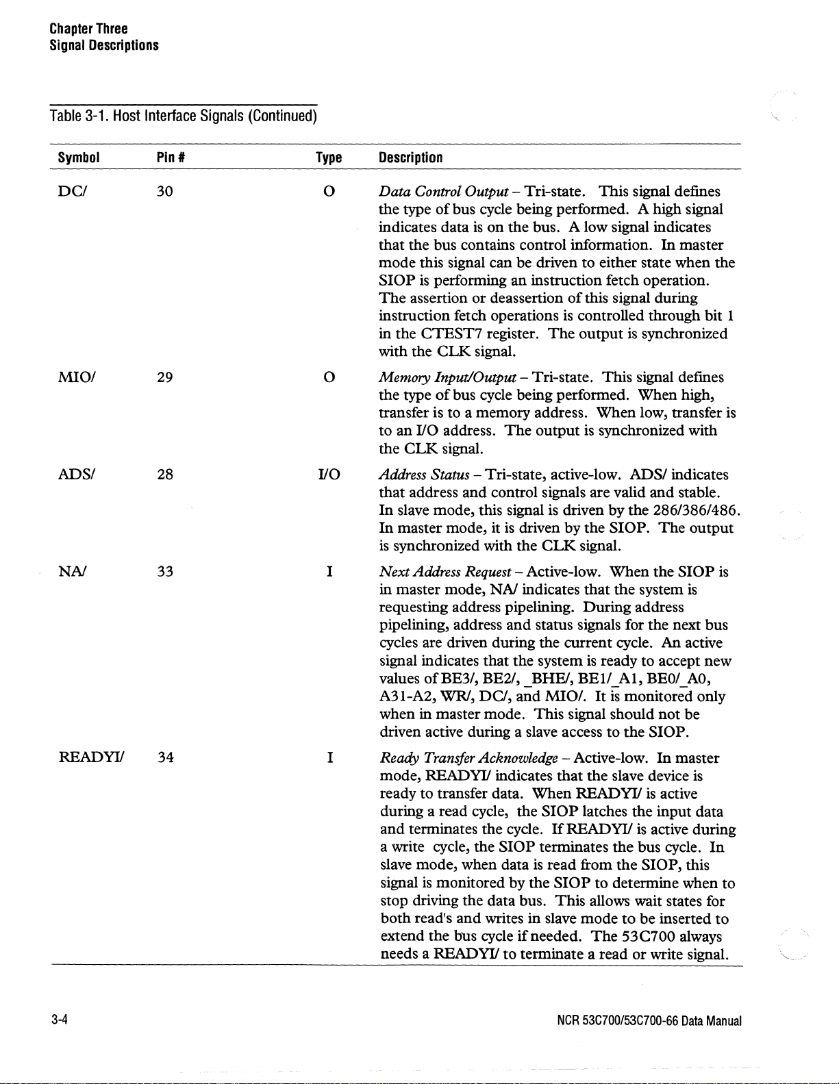
Table
Symbol
DCI
MIOI
ADSI
3-1.
Host
Interface
Pln#
Signals
(Continued)
30
29 a
28
Type
a
I/O
Description
Data
Control Output - Tri-state.
the
type
of
bus
cycle being performed. A high signal
data
is
indicates
that
the
mode
SlOP
The
this signal
is
assertion
bus contains control information.
performing
on
can
or
deassertion
the
bus. A low signal indicates
be
driven
an
instruction fetch operation.
This
signal defines
to
either state when
of
this signal during
In
master
instruction fetch operations is controlled through
in
the
CTEST7
with the
Memory Input/Output - Tri-state.
the
type
CLK
of
transfer is to a memory address.
to
an
I/O
address.
the
CLK
signal.
Address Status - Tri-state, active-low.
that
address
In
slave
mode,
In
master
is
synchronized with
register.
The
output
signal.
This
bus cycle being performed.
When
The
output
and
control signals are valid
this signal is driven
mode, it is driven
the
CLK
is synchronized with
by
by
the
signal.
is
synchronized
signal dermes
When
low, transfer is
ADSI
and
the
286/386/486.
SlOP.
The
high,
indicates
stable.
output
the
bit
\
",
I
NN
READYII
33 I
34
Next
Address Request - Active-low.
in master mode,
NAt
indicates
requesting address pipelining.
pipelining, address
cycles are driven during
signal indicates
values
ofBE3/,
A31-A2, WRf,
when
in
master
and
status signals for
the
that
the
system
BE2/, _BHFJ,
DC!,
and
MIO/.
mode.
This
current
driven active during a slave access
I
Ready Transfer Acknowledge - Active-low.
mode, READYII indicates
ready
to
transfer data.
during a read cycle,
and
terminates
a write cycle,
slave
mode,
is
signal
monitored by
stop driving
both
read's
extend
the
needs a READYII
the
the
SlOP
when
data
the
data bus.
and
writes
bus cycle
to
cycle.
that
When
the
SlOP
If
READYII
terminates
is
read
the
SlOP
This
in
slave
if
needed.
terminate a read
When
that
During
is
ready to accept
BEll_AI,
It
is
signal should
to
the
the
system
address
the
next
cycle.
An
BEO/_AO,
monitored only
not
the
SlOP.
In
the
slave device
READYII
latches
from
to
is
active
the
input
is
active during
the
bus cycle.
the
SlOP,
determine
allows wait states for
mode
The
to
be
inserted
53C700
or
write signal.
SlOP
is
bus
active
new
be
master
is
data
In
this
when
always
is
to
to
3-4
NCR
53C700/53C700-66
Data
Manual
Page 31
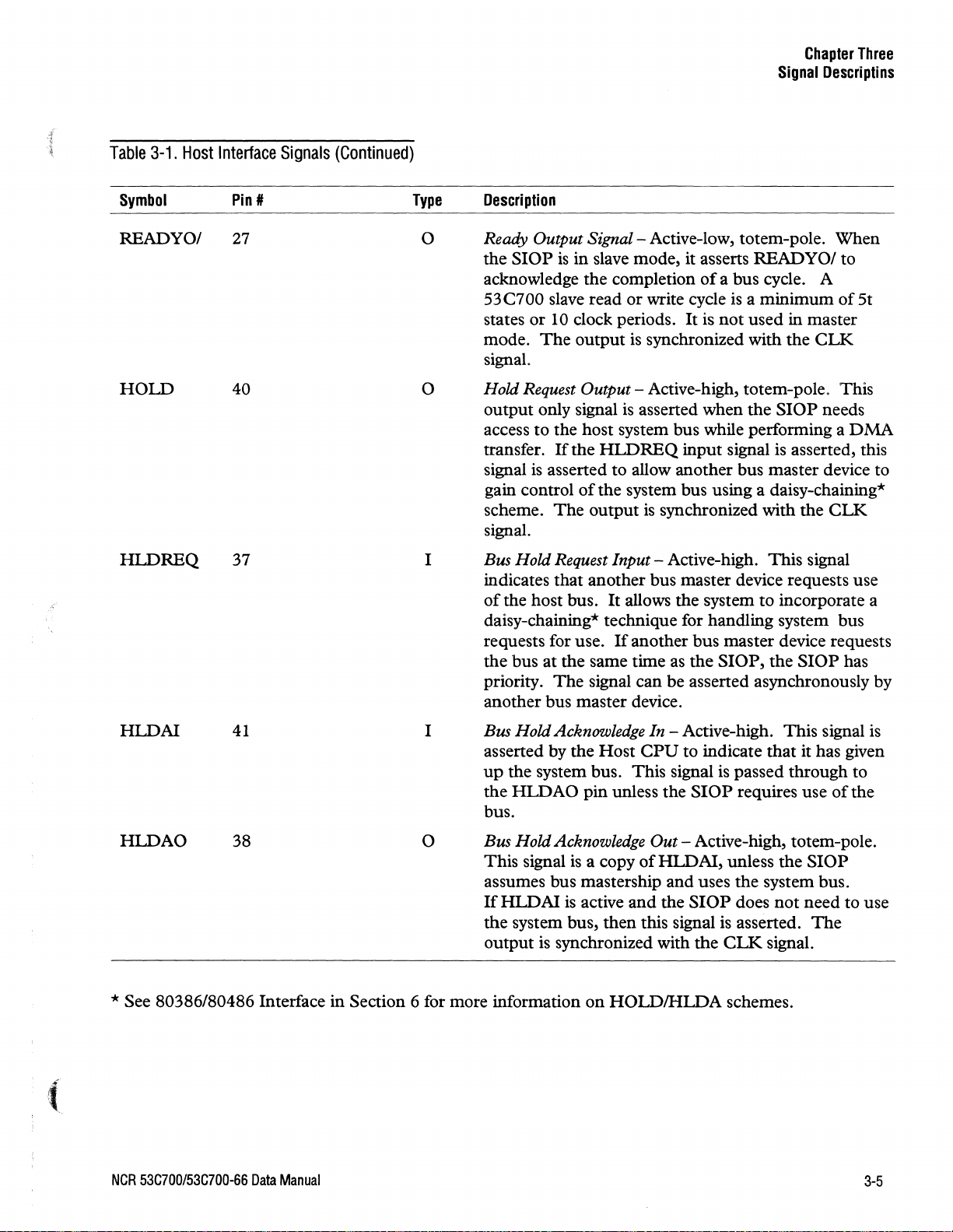
·1
.~
Table
Symbol
3-1.
Host
Interface
Pin
##
Signals
(Continued)
Type
Description
Chapter
Signal
Three
Descriptins
READYOI
27
0
Ready Output
SlOP
the
Signal-
is
in slave mode, it asserts
Active-low, totem-pole. When
acknowledge the completion
53C700 slave read
or
10
states
mode.
clock periods.
The
output
or
write cycle
It
is
synchronized with the
READYOI
of
a bus cycle.
is
a minimum
is
not
used in master
to
A
of
CLK
5t
signal.
HOlD
40
0
Hold Request Output - Active-high, totem-pole. This
output only signal
to
access
transfer.
signal
the host system bus while performing a
If
the
is
asserted to allow another bus master device to
gain control
scheme.
The
is
asserted when the
HillREQ
of
the system bus using a daisy-chaining*
output
input signal
is
synchronized with the
SlOP
needs
is
asserted, this
CLK
DMA
signal.
HillREQ
37 I
Hold Request Input - Active-high.
This
signal
Bus
indicates that another bus master device requests use
of
,::
the host bus.
It
allows the system to incorporate a
daisy-chaining* technique for handling system bus
If
requests for use.
the bus at the same time
priority.
The
another bus master device requests
as
the
SlOP,
the
SlOP
has
signal can be asserted asynchronously by
another bus master device.
(
HillA!
41
I
Bus
asserted by the Host
up
the
bus.
HillAO
38 0
Bus Hold Acknowledge
This signal
assumes bus mastership and uses the system bus.
If
the system bus, then this signal
output
* See
80386/80486 Interface in Section 6 for more information
NCR
53C700/53C700-66
Data
Manual
Hold Acknowledge
In
- Active-high. This signal
CPU
to indicate that it has given
the system bus. This signal
HillAO
HLDA!
pin unless the
Out
is
a copy
is
active
is
synchronized with the
on
of
HillA!,
and
the
HOIDIHIDA
SlOP
- Active-high, totem-pole.
SlOP
is
passed through to
requires use
unless the
does
is
asserted.
CLK
SlOP
not
need to use
signal.
The
schemes.
of
is
the
3-5
Page 32
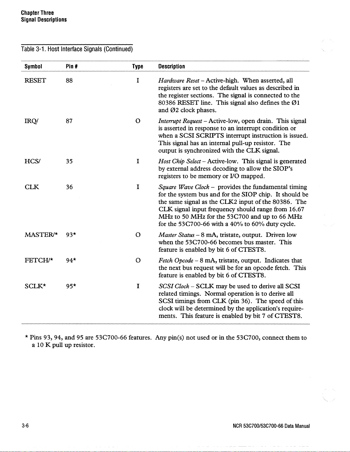
Chapter
Signal
Descriptions
Table
3-1.
Three
Host
Interface
Signals
(Continued)
Symbol
RESET
IRQ!
HCS!
CLK
Pin'
Type
88
87
35 I
36
I
o
I
Description
Hardware Reset - Active-high.
registers are set
the register sections.
80386
and
Interrupt Request - Active-low,
is
when a
This
output
Host Chip
RESET
02
clock phases.
asserted in response
SCSI
signal has
is
to
the
default values as described in
The
line.
This
to
SCRIPTS
an
internal pull-up resistor.
synchronized with the
Select-
Active-low.
by external address decoding to allow
registers to
Square Wave Clock - provides
for the system bus
the
same signal as
CLK
MHz
be
memory
and
the
or
for
CLK2
signal input frequency should range from 16.67
to
50
MHz
for the
for the 53C700-66 with a
When
signal
asserted, all
is
connected
signal also defines
open
drain. This signal
an
interrupt condition or
interrupt instruction is issued.
CLK
signal.
This
signal
the
I/O mapped.
the
fundamental timing
the
SlOP
chip.
input
ofthe
53C700
40%
to
and
60%
up
duty
to
the
The
is
generated
SlOP's
It
should be
80386.
to 66
MHz
cycle.
the
01
The
MASTERI* 93*
FETCHI*
SCLK*
* Pins 93, 94,
a
10K
pull
94*
95*
and
up
resistor.
0
a
Master Status - 8 rnA, tristate,
when
the
feature
Fetch Opcode - 8 rnA, tristate, output. Indicates
is
the next bus request will
feature
I
SCSI
is
Clock -
related timings. Normal operation
SCSI
timings from
clock will be determined by the application's require-
ments.
This
95 are 53C700-66 features. Any pines)
output.
Driven low
53C700-66 becomes bus master.
enabled
enabled
not
by
bit 6
of
CTEST8.
be
for
an
opcode fetch. This
by
bit 6
of
CTEST8.
SCLK
may
CLK
be
used
(pin 36).
to
derive all
is
to
The
feature is enabled by bit 7
used
or
in
the 53C700, connect
derive all
speed
of
This
that
SCSI
of
this
CTEST8.
them
to
3-6
NCR
53C700/53C700-66
Data
Manual
Page 33
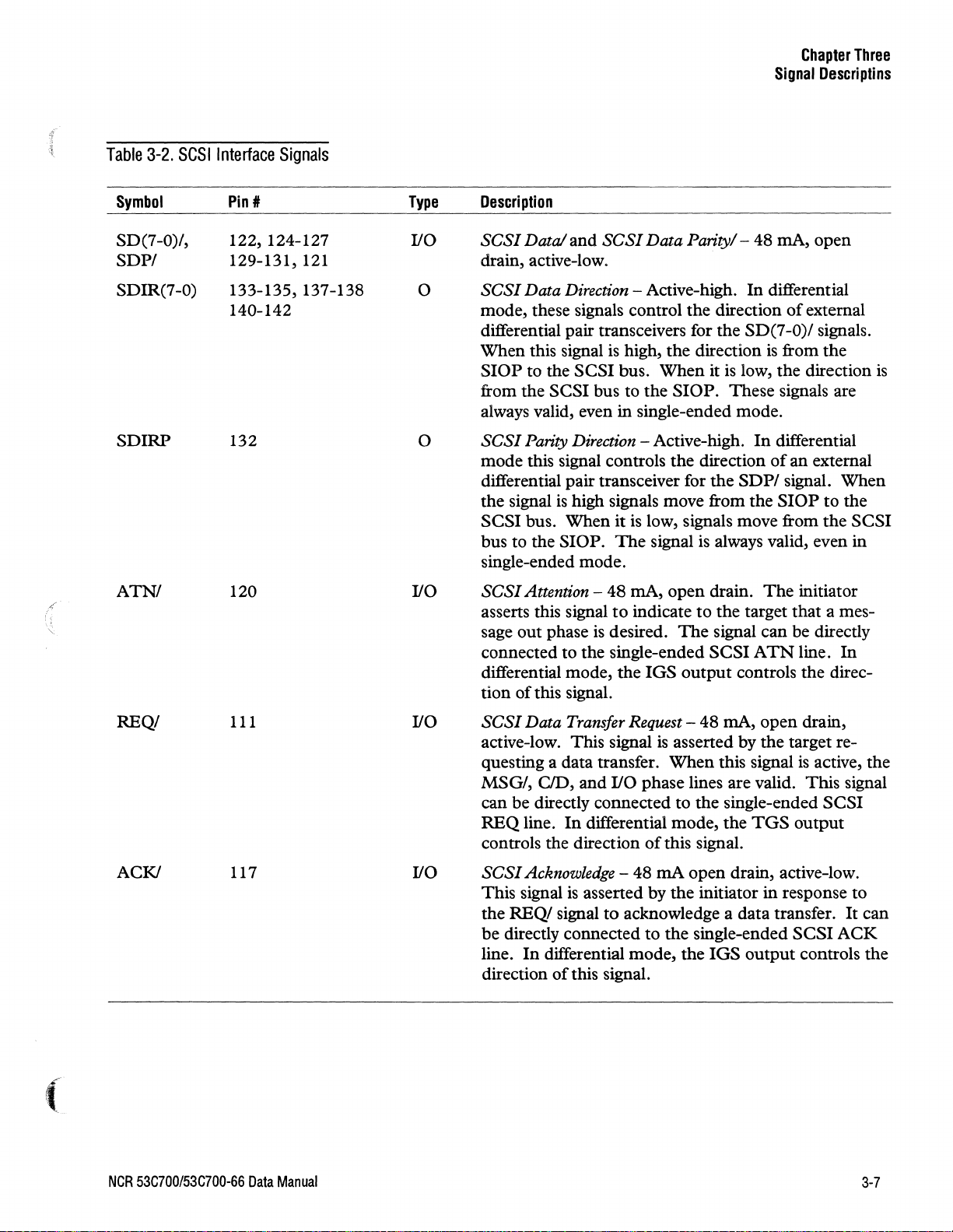
Table
3-2.
SCSI
Interface
Signals
Chapter
Signal
Three
Descriplins
,;
\~,
Symbol
Pint
SD(7-0)/, 122, 124-127
SDP/
SDIR(7-0)
129-131,
121
133-135, 137-138
140-142
SDIRP
ATN/
132
120 I/O
Type
I/O
0
0
Description
SCSI
Datal
and
SCSI
Data Parity/ - 48 rnA, open
drain, active-low.
SCSI
Data Direction - Active-high.
mode, these signals control the direction
In
differential
of
external
differential pair transceivers for the SD(7-0)/ signals.
is
When this signal
SlOP
to the SCSI bus. When it
high, the direction
from the SCSI bus to the
SlOP.
is
from the
is
low, the direction
These signals are
always valid, even in single-ended mode.
SCSI
Parity Direction - Active-high.
mode this signal controls the direction
differential pair transceiver for the
is
the signal
SCSI bus. When
bus to the SlOP.
high signals move from the
it
is
low, signals move from
The
signal
is
In
differential
of
an external
SDP/
signal. When
SlOP
to the
the
SCSI
always valid, even in
single-ended mode.
SCSI
Attention - 48 rnA, open drain.
to
asserts this signal
sage out phase
indicate to the target that a mes-
is
desired.
The
connected to the single-ended
differential mode, the
of
tion
this signal.
IGS
output
signal can be directly
SCSI
The
initiator
ATN
line.
In
controls the direc-
is
REQI
111
ACKI 117
I/O
I/O
SCSI
Data Transfer Request - 48 rnA, open drain,
is
active-low. This signal
questing a data transfer.
MSG/, C/O, and
I/O phase lines are valid.
can be directly connected to the single-ended
REQ
line.
In
differential mode, the
controls the direction
SCSI
Acknowledge - 48 rnA open drain, active-low.
is
This signal
asserted by the initiator
asserted by the target re-
When
this signal
TGS
of
this signal.
in
response to
is
active, the
This
SCSI
output
the REQI signal to acknowledge a data transfer.
be directly connected to the single-ended
line.
In
direction
differential mode, the
of
this signal.
IGS
output controls the
SCSI
signal
It
can
ACK
NCR
53C700/53C700-66
Data
Manual
3-7
Page 34
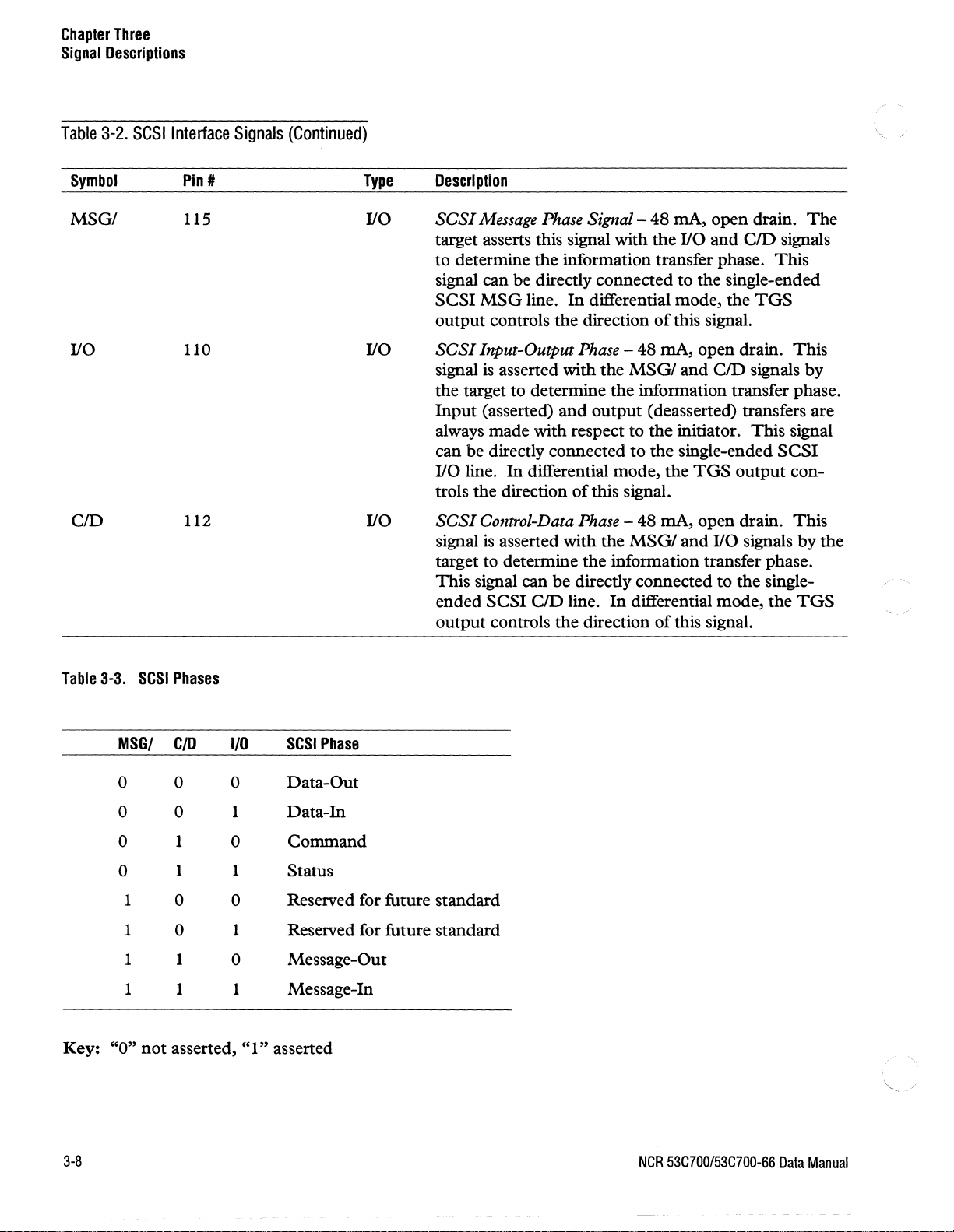
Chapter
Signal
Descriptions
Table
3-2.
Symbol
Three
SCSI
Interface
Pin
#
Signals
(Continued)
Type
Description
MSG/
I/O
CID
115
110
112
I/O
I/O
I/O
SCSI
Message Phase
target asserts this signal with the I/O and
Signal-
48 rnA, open drain.
CID
signals
The
to determine the information transfer phase. This
signal can be directly connected to the single-ended
SCSI
MSG
output controls the direction
SCSI
Input-Output Phase - 48 rnA, open drain.
signal
line.
In
is
asserted with the
differential mode, the
of
this signal.
MSG/
and
CID
TGS
This
signals by
the target to determine the information transfer phase.
and
Input (asserted)
output (deasserted) transfers are
always made with respect to the initiator. This signal
can be directly connected to the single-ended
I/O line.
trols the direction
SCSI
signal
In
differential mode, the
of
this signal.
Control-Data Phase - 48 rnA, open drain. This
is
asserted with the
MSG/
TGS
and I/O signals by the
SCSI
output con-
target to determine the information transfer phase.
This signal can be directly connected to the single-
ended
output controls the direction
SCSI
CID
line.
In
differential mode, the
of
this signal.
TGS
Table
Key:
3-3.
SCSI
MSGI
0
0 0
0
0
1
1
1
1 1
"0"
not
Phases
CID
0
1
1
0
0
1
asserted,
110
0
1
0
1
0
1
0
1
"1"
SCSI
Phase
Data-Out
Data-In
Command
Status
Reserved for future standard
Reserved for future standard
Message-Out
Message-In
asserted
,~.
""',
""-._./
3-8
NCR
53C700/53C700-66
Data
Manual
Page 35
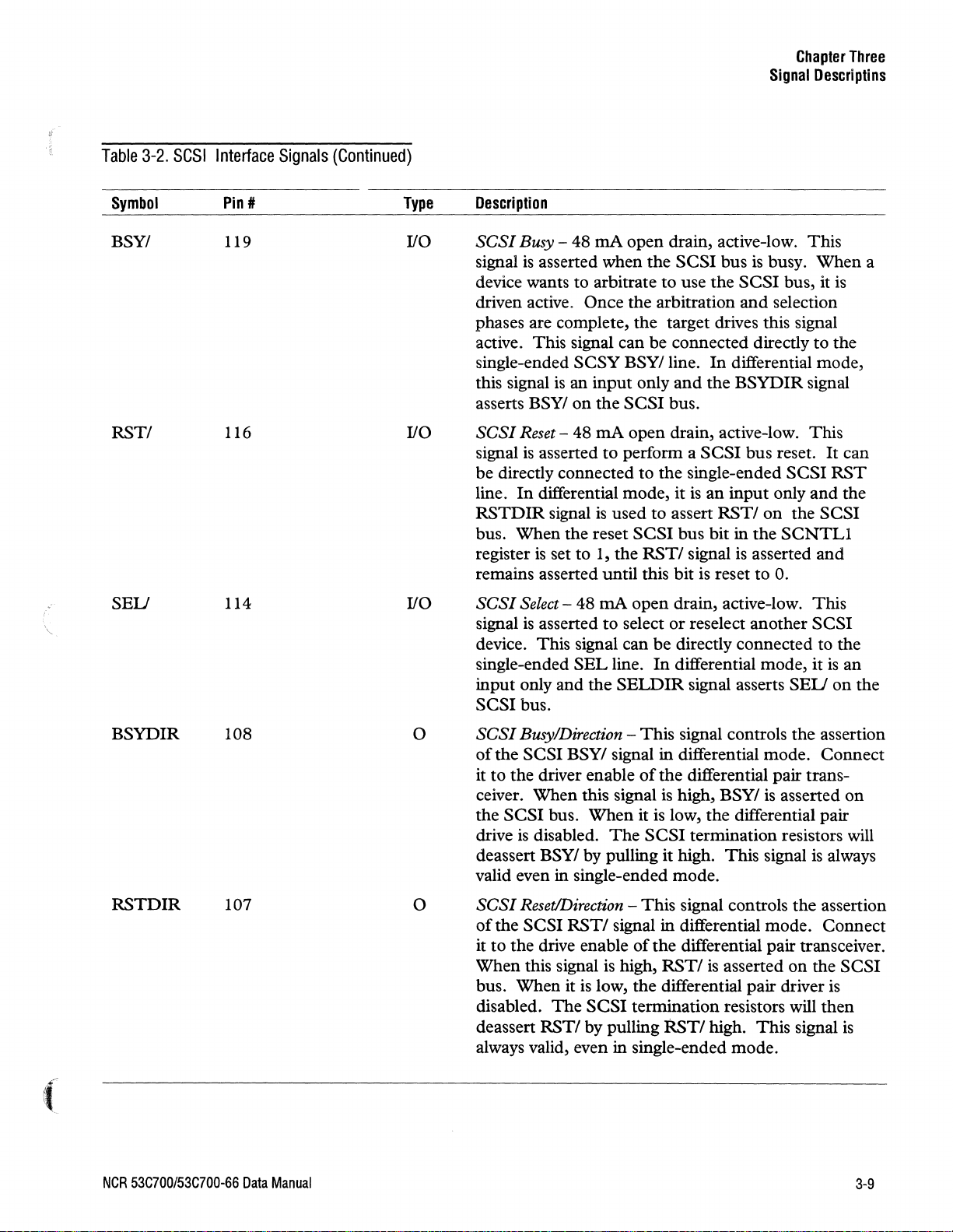
Table
3-2.
SCSI
Interface
Signals
(Continued)
Chapter
Signal
Three
Descriptins
Symbol
BSYI
RSTI
SEU
Pin
119
116
114
##
Type
I/O
I/O
I/O
Description
SCSI
Busy - 48 rnA open drain, active-low. This
signal
device wants to arbitrate to use the
driven active. Once
phases are complete, the target drives this signal
active. This signal can
single-ended
this signal
asserts
SCSI
signal
be
line.
RSTDIR
bus.
register
remains asserted until this bit is reset to
SCSI
signal
device. This signal can
single-ended
input only and
SCSI
is
asserted when
SCSY
is
an
input
BSYI
on
the
Reset - 48 rnA open drain, active-low. This
is
asserted
directly connected to
In
differential mode, it
signal
When
is
Select - 48
is
asserted
bus.
is
the reset
set to 1, the
rnA
SEL
the
the
SCSI
the
arbitration
be
connected directly
BSY/line.
only
and
SCSI
bus.
to
perform a
the
single-ended
used to assert
SCSI
bus bit in
RSTI
signal
open
drain, active-low.
to
select
line.
SELDIR
or
be
directly connected to the
In
differential mode,
signal asserts
bus
is
busy.
SCSI
bus, it
and
selection
In
differential mode,
the
BSYDIR
SCSI
bus reset.
SCSI
is
an
input
only
RSTI
on
the
the
SCNTL1
is
asserted
O.
reselect another
SEU
When
to
signal
It
and
SCSI
and
This
SCSI
it
is
is
the
can
RST
the
an
on
the
a
(
BSYDIR
RSTDIR
NCR
53C700/53C700-66
108
107
Data
Manual
o
o
SCSI
Busy/Direction -
of
the
SCSI
BSYI signal in differential mode.
it
to
the driver enable
ceiver. When this signal
the
SCSI
bus.
When
drive
is
disabled.
deassert
valid even in single-ended mode.
SCSI
of
it
to
When
bus. When it is low, the differential pair driver is
disabled.
deassert
always valid, even in single-ended mode.
BSYI by pulling it high. This signal
ResetlDirection -
the
SCSI
RSTI
the drive enable
this signal
The
SCSI
RSTI
by pulling
This
signal controls
of
the
differential pair trans-
is
high, BSYI
it is low, the differential pair
The
SCSI
termination resistors will
This
signal controls
signal in differential mode. Connect
ofthe
is
high,
termination resistors will
differential pair transceiver.
RSTI
is
asserted on the
RsTI
high.
is
asserted
This
the
assertion
Connect
is
the
assertion
then
signal
always
on
SCSI
is
3-9
Page 36
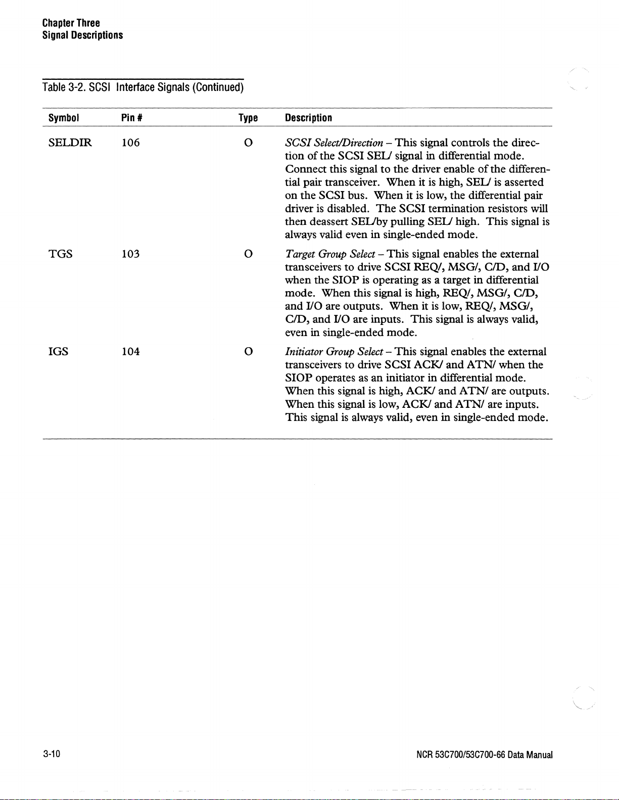
Chapter
Signal
Descriptions
Table
3-2.
Three
SCSI
Interface
Signals
(Continued)
Symbol
SELDIR
TGS
IGS
Pin'
106
103
Type
o
o
104 o
Description
SCSI
SelectlDirection
of
tion
Connect this signal
tial pair transceiver. When it
on
driver
then deassert
always valid even in single-ended mode.
Target
transceivers to drive
when the
mode. When this signal
and I/O are outputs. When it
the SCSI
the SCSI bus. When it
is
disabled.
SEUby
Group
Select
SlOP
CID, and I/O are inputs. This signal
even in single-ended mode.
Initiator
transceivers to drive
SlOP
When this signal
When this signal
This signal
Group
operates
is
always valid, even in single-ended mode.
- This signal controls the direc-
SEU
signal in differential mode.
to
the driver enable
is
high,
SEU
is
low, the differential pair
The
SCSI
termination resistors will
pulling
SEU
high. This signal
- This signal enables the external
SCSI
REQ/, MSG/, CID,
is
operating
Select
- This signal enables the external
SCSI
as
an
initiator in differential mode.
is
high, ACKI
is
low, ACKI
as
a target in differential
is
high, REQ/,
is
low, REQ/,
is
ACKI and
and
and
ATNI
ATNI
A
TNI
of
the
differen-
is
asserted
and
I/O
MSG/,
CID,
MSG/,
always valid,
when the
are outputs.
are inputs.
is
3-10
NCR
53C700/53C700-66
Data
Manual
Page 37
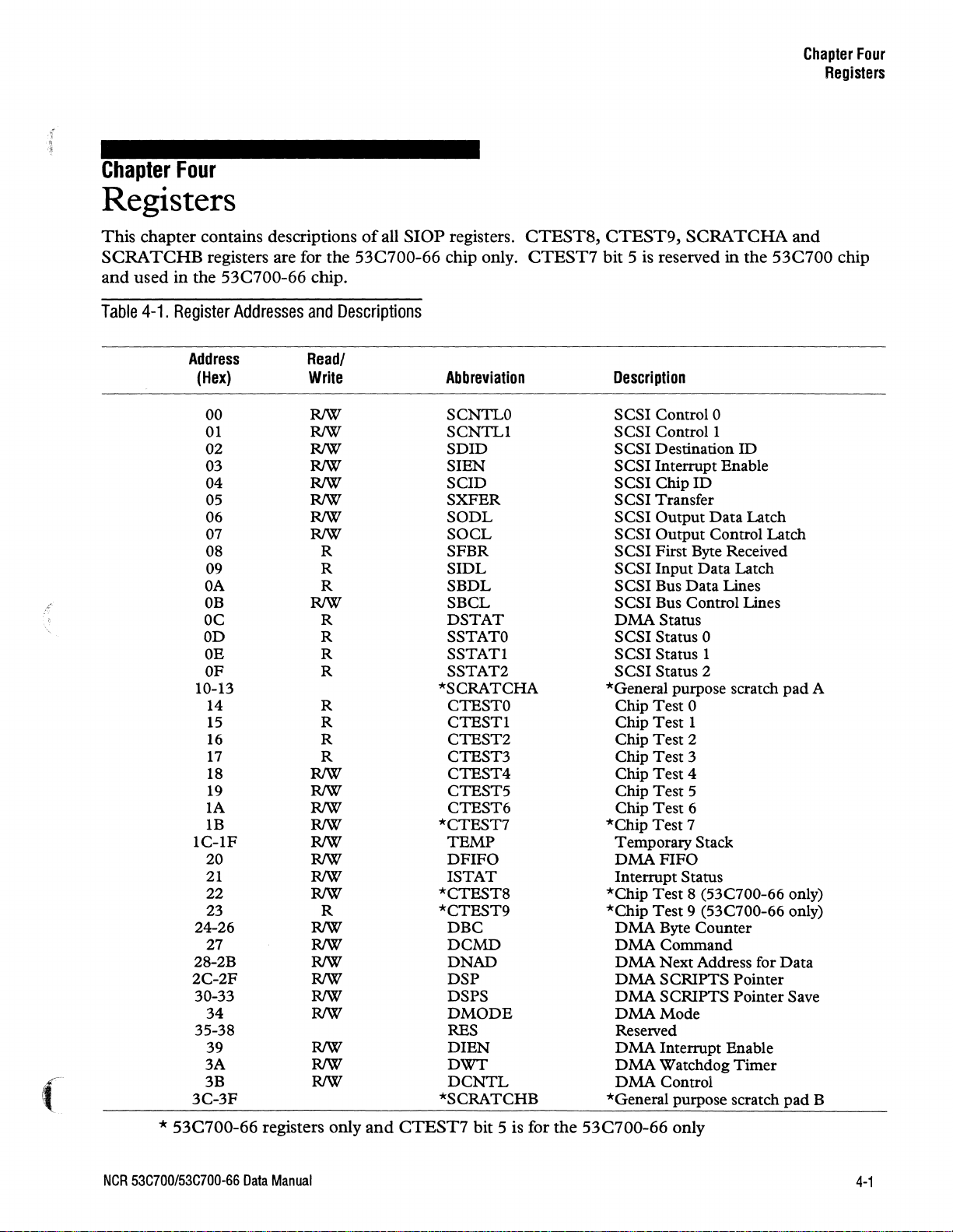
This
SCRA
and
used
Table
chapter
TCHB
in
4-1.
Register
contains
registers
the
53C700-66
Addresses
descriptions
are
for
the
chip.
and
Descriptions
of
all
SlOP
53C700-66
registers.
chip
only.
CTEST8,
CTEST7
CTEST9,
bit
5 is reserved
SCRATCHA
in
the
53C700
Chapter
Registers
and
Four
chip
:f
"
(-
Address
(Hex)
00 RIW SCNTLO
01
02 RIW
03 RIW
04
05
06 RIW
07
08 R
09
OA
OB
OC
OD
OE
OF
10-13 *SCRATCHA *General purpose scratch
14 R
15
16 R
17
18
19
lA
IB
lC-IF
20
21
22
23
24-26
27
28-2B
2C-2F
30-33
34
35-38
39
3A
3B RIW
3C-3F
Readl
Write
RIW
RIW
RIW
RIW
R SIDL SCSI Input Data Latch
R SBDL SCSI Bus Data Lines
RIW SBCL
R
R SSTATO SCSI Status 0
R SSTATI SCSI Status 1
R SSTAT2 SCSI Status 2
R
R CTEST3 Chip Test 3
RIW
RIW CTEST5 Chip
RIW
RIW
RIW
RIW
RIW
RIW *CTEST8 *Chip Test 8 (53C700-66 only)
R
RIW
RIW
RIW DNAD
RIW
RIW
RIW
RIW
RIW
Abbreviation
SCNTLI
SDID SCSI Destination ID
SIEN SCSI Interrupt Enable
SCID SCSI
SXFER SCSI Transfer
SODL
SOCL
SFBR SCSI First Byte Received
DSTAT
CTESTO Chip Test 0
CTESTI
CTEST2
CTEST4 Chip Test 4
CTEST6
*CTEST7
TEMP
DFIFO
ISTAT
*CTEST9
DBC
DCMD
DSP
DSPS
DMODE
RES Reserved
DIEN
DWT
DCNTL
*SCRATCHB
Description
SCSI
Control 0
SCSI Control 1
ChipID
SCSI Output
SCSI Output Control Latch
SCSI
Bus Control Lines
DMAStatus
Chip
Test
Chip Test 2
Test
Test
Chip
*Chip
Test
Temporary Stack
DMAFIFO
Interrupt Status
*Chip
Test
DMA
Byte Counter
DMACommand
DMA
Next Address for
DMA
SCRIPTS Pointer
DMA
SCRIPTS Pointer Save
DMAMode
DMA
Interrupt Enable
DMA
Watchdog
DMA
Control
*General purpose scratch
Data
Latch
1
5
6
7
9 (53C700-66 only)
Timer
pad
Data
pad
A
B
*
53C700-66
NCR
53C700/53C700-66
registers only
Data
Manual
and
CTEST7
bit
5 is for
the
53C700-66
only
4-1
Page 38
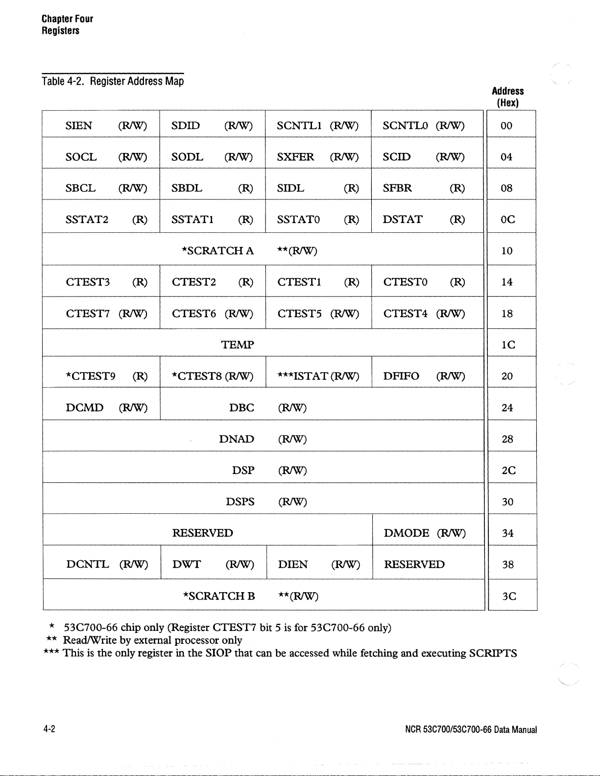
Chapter
Registers
Table
Four
4-2.
Register
Address
Map
Address
(Hex)
smN
SOCL
SBCL
SSTAT2
CTEST3
CTEST7
*CTEST9
DCMO
(RIW)
(RIW)
(RIW)
(R)
(R)
(RIW)
(R)
(RIW)
SDID
SODL
(RIW)
(RIW)
SBDL
SSTATI
*SCRATCHA
CTEST2
CTEST6
(RIW)
TEMP
*CTEST8
(RIW)
(R)
(R)
(R)
DBC
SCNTLI
SXFER
SIDL
SSTATO
(RIW)
(RIW)
(R)
(R)
**(RIW)
CTESTI
CTEST5
(R)
(RIW)
***ISTAT (RIW)
(RIW)
SCNTLO
SCID
SFBR
DSTAT
CTESTO
CTEST4
DFIFO
(RIW)
(RIW)
(R)
(R)
(R)
(RIW)
(RIW)
00
04
08
OC
10
14
18
IC
20
24
'-
.,/
RESERVED
DCNTL
(RIW)
DW!'
*SCRATCHB
53C700-66 chip only (Register
*
**
ReadIWrite by external processor only
*** This
is
the only register in the
DNAD
DSP
DSPS
(RIW)
(RIW)
(RIW)
DMODE
(RIW)
DmN
(RIW)
RESERVED
**(RIW)
CTEST7
SlOP
bit 5
is
for 53C700-66 only)
that can be accessed while fetching and executing
(RIW)
28
2C
30
34
38
3C
SCRIPTS
4-2
NCR
53C700/53C700-66
Data
Manual
Page 39
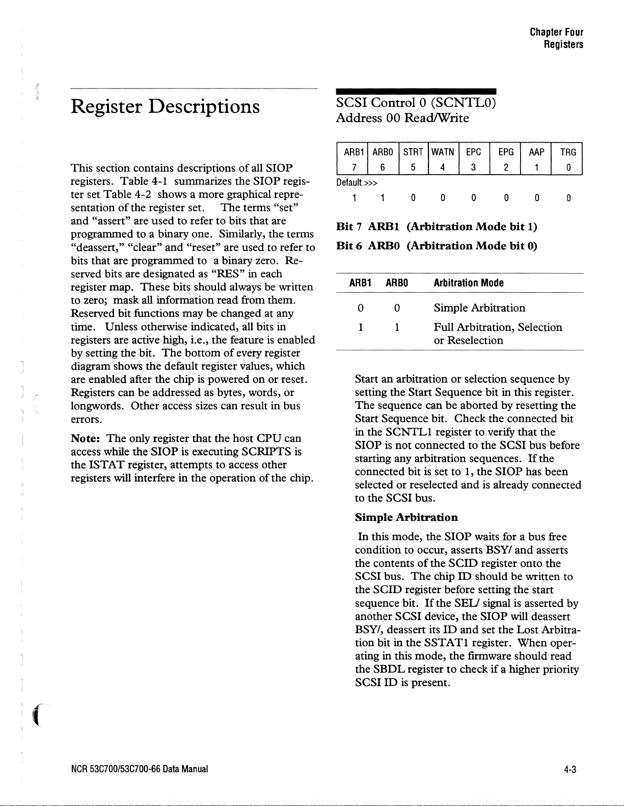
Chapter
Registers
Four
Register Descriptions
SCSI
Control 0 (SCNTLO)
Address 00 ReadIWrite
ARBO
ARB1
This section contains descriptions
of
registers. Table 4-1 summarizes the
all
SlOP
SlOP
regis-
7
Default
»>
ter set Table 4-2 shows a more graphical repre-
of
sentation
the register set.
and "assert" are used to refer to bits that are
programmed to a binary one . Similarly, the terms
"deassert," "clear" and "reset" are used to refer to
The
terms "set"
Bit 7 ARBI
Bit
6 ARBO
bits that are programmed to a binary zero. Reserved bits are designated
register map. These bits should always be written
all
to zero; mask
information read from them.
Reserved bit functions may be changed at any
time. Unless otherwise indicated, all bits in
registers are active high, i.e., the feature
by setting the bit.
1
J
diagram shows the default register values, which
The
are enabled after the chip
Registers can be addressed as bytes, words,
longwords. Other access sizes can result in bus
errors.
Note:
access while the
the
registers
The
only register that the host
SlOP
ISTAT
register, attempts to access other
will interfere in the operation of the chip.
as
"RES" in each
bottom
of
every register
is
powered on or reset.
CPU
is
executing SCRIPTS
is
enabled
or
can
is
ARB1
o 0
1 1
Start an arbitration or selection sequence by
setting the Start Sequence bit in this register.
The
Start Sequence bit. Check the connected bit
in the
SlOP
starting any arbitration sequences.
connected bit
selected or reselected and
to the SCSI bus.
STRT
WATN
6 5 4 3 2 1
o o o o
(Arbitration
(Arbitration
ARBO
Arbitration
EPC
Mode
Mode
Mode
EPG
bit
bit
AAP
o
1)
0)
TRG
0
o
Simple Arbitration
Full Arbitration, Selection
or Reselection
sequence can be aborted by resetting the
SCNTLI
is
not connected to the SCSI bus before
register to verify that the
is
set to 1, the
SlOP
has been
is
already connected
If
the
NCR
53C700/53C700-66
Data
Manual
Simple
In
condition to occur, asserts
the contents
SCSI bus.
the
sequence bit.
another SCSI device, the
BSY/, deassert its
tion bit in the
Arbitration
this mode, the
ofthe
The
chip
SCID
register before setting the start
If
the
SSTATI
SlOP
waits for a bus free
BSYI
SCID
register onto the
ID
should be written to
SEU
signal
SlOP
ID
and
set the Lost Arbitra-
register. When oper-
and
asserts
is
asserted by
will deassert
ating in this mode, the firmware should read
SBDL
the
SCSI
ID
register
is
present.
to
check
if
a higher priority
4-3
Page 40
Chapter
Registers
Four
The
programming sequence is as follows:
1. Clear low-level
2. Set
3. Enable simple arbitration (reset
4.
5. Wait for either:
6.
7. Wait for
8.
9. Wait
10.
11.
53C700
SODL
bit 6 and
Start
SCNTLO
A. Arbitration in progress
= 1)
B.
C.
If
Goto
Iflost
goto step 7
If
our
SBDL) goto step 13
register)
simple arbitration sequence, (set
or
Lost
arbitration
SEL
arbitration
SEL
step 4
2400
arbitration
our
10
ID
with any other
mode
chip
7)
bit 5)
asserted
in
progress, goto step 9
deasserted
ns
is
the
highest asserted (compare
bit
ID
(SCID
(SSTATI
(SBCL
(SSTATI
IDs
register
(SSTATI
bit 4 = 0)
(SBCL
bit
present
and
SCNTLO
bit 4
bit
3 =
1)
bit 4 = 0)
3 = 1)
in
or
24. Set
25.
26. Wait
27. Deassert
28. Wait
29. Wait for either:
30.
31. Clear assert
32. Wait
33.
34. Clear connected bit (clear.
35.
SODL
destination
If
initiator, set
bit 3)
BSY asserted
A.
B.
Timeout
determine by
through this loop)
IfBSY
37
bit 6)
IfBSY
step
37
Clear
to
bitwise
ID
ATN
90 ns
BSY (clear
400
ns
(SBCL
(250 ms recommended,
maximum
was asserted (step 29-A) goto step
data
201
JlS
is asserted
SOCL
register
OR
if
SOCL
bus
bit
(SBCL
desired (set
bit 5 = 1)
number
(clear
of
chip
bit
5)
SCNTLI
bit
5 = 1) goto
SCN1Ll
ID
and
SOCL
or
times
bit
4)
12.
Goto
step 10
13. Assert BSY (set
14.
If
target
15. Set assert
16. Set connected bit (set
17. Assert
4)
18.
If
goto step 22
19. Clear
20. Clear assert
SCNTLI
21.
Goto
22. Wait
23. Clear start sequence
bit
mode,
data
BSY
not
lost arbitration
SOCL
step 7
1200 ns
5)
bus
and
register
data
bits 6
SOCL
set 110 (set
bit
SEL
bus, connected bits (clear
and
bit
5)
SOCL
(set
SCN1Ll
SCN1Ll
(set
SOCL
(SSTATI
4)
bit
(clear
bit
0)
bit
bit
4)
bits 5
and
bit
3 = 0)
SCN1LO
6)
36.
Goto
step 4
SEL
(clear
37. Deassert
38. Clear assert
bit 6)
39. Proceed with information transfers
(SCRIPTS
Full
Arbitration,
In
this
mode,
condition,
SCSI
10
(the highest priority
SCID
SEU
or
SlOP
wait until
tion again.
it wins control
register)
signal
if
the
SlOP
will deassert BSY/, deassert its
data
or
the
then
it asserts BSYI
onto
is
asserted by
detects a higher priority
the
next
The
SlOP
of
the
SOCL
bus bit (clear
low-level)
Selection & Reselection
SlOP
waits for a
the
SCSI
bus
free state to try arbitra-
repeats arbitration
SCSI
bit
and
ID
bus.
another
bus.
4)
SCNTLI
bus
asserts its
stored in
If
SCSI
free
the
10,
ID,
the
device
the
and
until
4-4
NCR
53C700/53C700-66
Data
Manual
Page 41
Chapter
Registers
Four
(
When the
Arbitration Bit
After winning arbitration, the
selection by asserting the following onto the
SCSI
SDID
priority
a selection
plete bit
a selection time-out occurs, the Selection
Time-out bit
ter.
The
1.
SCID
2.
SDID
3. SCNTLO = full arb, selection (bit 6, 7)
4.
SCNTLO = start sequence, full arb,
selection (bit
5. Wait for function complete or select timeout
or
Bit S START
When this bit
tration
SlOP
the Arbitration
SCSI
controlled by the
Use the Start Sequence bit in low-level mode
or
register level programming.
sequence must be completed (chip connected,
SCNTL1,
mode
pected disconnect
cleared automatically when the selection
sequence
The
resetting this bit to
aborted, check the connected bit in the
SCNTL1
SlOP
connected bit
has won arbitration.
SlOP
wins arbitration, the
is
set in the SSTAT1 register.
SlOP
bus:
SEU,
register)
ID
stored in the
is
is
set to 1 in the SSTATO register.
programming sequence
= chip
= target
SST A TO
select time-out (bit 5)
or
selection sequences will start.
will arbitrate and/or select according to
SCRIPTSTM, the Start Sequence
bit 4) before initializing low-level
(DCNTL,
is
arbitration sequence can be aborted by
register, bit 4, to verify that the
is
not
the target's
and
the
complete, the Function Com-
is
set to 1 in
ID
ID
7,
6, 5)
ID
SlOP's
SCID
the
is
SST A TO
as
= function complete (bit 6)
(Start
is
written to 1, one
Mode
SCRIPTS
bit 3). Otherwise,
complete.
connected on the
is
set to indicate that
Sequence)
bits. While executing
PROCESSOR.
will occur. This bit
O.
If
the
sequence
SCSI
Won
performs
(stored in the
ID
(the highest
register). After
regis-
follows:
ofthe
The
start
an
is
bus.
the
arbi-
The
is
unex-
is
The
SlOP
If
Bit 4 WATN
When set to 1, the SCSI
asserted during the selection phase.
asserted when BSY!
target device. When executing
SCRIPTS,
SCRIPTS
low-level mode
While attempting to select a target device
a selection time-out occurs, A
deasserted when
A
TN!
signal
the Select with A
Bit 3 EPC
When set to 1, the SCSI data bus
for odd parity when
The
host data bus
parity generation
Host
data bus parity
loaded into the
SCSI
data.
of
the SSTATO register
interrupt can be generated
If
the
SlOP
can stop bytes with parity errors written into
DMA
the
SCSI bus
If
the
SlOP
a parity error
be asserted (SCNTLO, bit 1).
continues until the target changes phase to
Message-Out indicating a parity error has been
detected.
the current
has executed and/or the target changes phase
to message out.
If
this bit
reported.
(Select
this bit
PROCESSOR. This bit
or
SEU
is
not
TN!
(Enable
SODL
If
a parity error
is
operating in target mode, you
FIFO
(SXFER
The
is
from being written to the
is
operating in initiator mode and
is
detected, A
parity error
SCRIPTS
written to 0, parity errors are not
with
ATNI
Sequence)
ATNI
is
deasserted
is
initialized by the
register level programming.
is
deasserted.
asserted during selection
bit
is
reset to
Parity
SCSI
data
is
checked for
is
disabled (SCNTLO, bit 2).
is
checked
register when sending
is
is
set to 1
(SmN,
register, bit 7 = 0).
TN!
is
reported when
Block Move instruction
on a Start
signal
SCSI
TN!
ATN!
to
select a
is
is
is
used in
The
o.
Checking)
is
checked
is
received.
odd
parity
as
data
is
detected, bit 0
and
an
bit 0).
can optionally
The
transfer
is
and
if
if
NCR
53C700/53C700-66
Data
Manual
4-5
Page 42
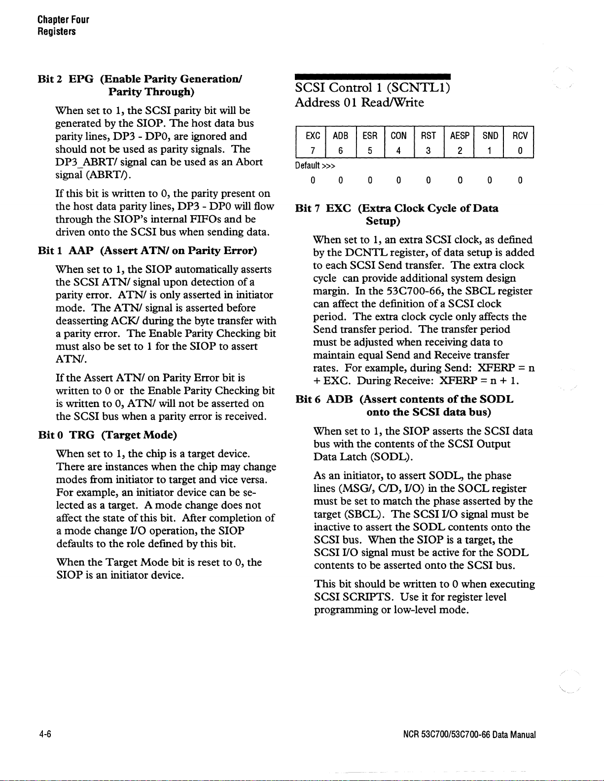
Chapter
Registers
Four
Bit 2 EPG
(Enable
Parity
When
generated
parity lines,
should
DP3
signal (ABRT/).
If
the
through
driven
Bit 1 AAP
When
the
parity error.
mode.
de asserting
a parity error.
must
ATN!.
If
written
is
the
Bit 0 TRG
When
There
modes
For
lected as a target. A
affect
a
defaults
When
SlOP
set
to
by
not
be
_ ABRT! signal can
this
bit
is
host data parity lines,
the
onto
(Assert
set
to
SCSI A TN!
The A TN!
also
be
the
Assert A
to 0 or
written
SCSI
to
bus
(Target
set
to
are
instances
from initiator
example,
the
state
mode
change 110 operation,
to
the
the
Target
is
an
Parity
Generation!
Through)
1,
the
SCSI
parity bit
the
SlOP.
DP3
- DPO, are ignored
used
written
SIOPts
the
SCSI
1,
the
signal
ATN!
ACKI
The
set
to
TN!
the
0,
A"IN! will
when
The
host
as parity signals.
be
used
to
0,
the
parity present
DP3
internal
bus
A
TN!
SlOP
is
only asserted in initiator
signal
during
Enable
1 for
on
Enable
a parity error
FIFOs
when sending data.
on
Parity
automatically asserts
upon
detection
is
asserted before
the
byte transfer with
Parity Checking
the
SlOP
Parity
Error
Parity Checking
not
Mode)
1,
the
chip is a target device.
when
the
to
target
an
initiator device can be se-
mode
of
this bit. After completion
role defmed
Mode
initiator device.
change does
by
bit
is reset
will
be
data
bus
and
The
as
an
Abort
on
- DPO will flow
and
be
Error)
of
a
bit
to
assert
bit
is
bit
be
asserted
is
chip may change
and
vice versa.
the
SlOP
this bit.
to
on
received.
not
0,
the
of
SCSI
Address
Default
Bit 7 EXC
Control 1
01
EXC
ADB
7 6 5 4 3
>>>
o
o
(SCNTLl)
ReadIWrite
ESR
CON
o
(Extra
Setup)
When
by
to
cycle
margin.
can affect
period.
Send
must
maintain
rates.
+
Bit 6 ADB
When
bus
Data
As
lines (MSG!, CID,
must
target (SBCL).
inactive
SCSI
SCSI
contents
This
SCSI
programming
set
to
1,
the
DCNTL
each
SCSI
can
provide additional system design
In
the
the
The
transfer period.
be
adjusted
equal
For
example,
EXC.
During
(Assert
onto
set
to
1,
with
the
contents
Latch
an
be
bit should
(SODL).
initiator,
set
to
to
assert
bus.
When
110 signal
to
be
SCRIPTS.
an
register,
Send
53C700-66,
definition
extra
Send
the
the
to
match
The
must
asserted
be
or
RST
AESP
o
Clock
when
Receive:
the
low-level
o
Cycle
extra
SCSI
of
data
transfer.
clock cycle only affects
The
and
during
contents
SCSI
SlOP
of
assert
110) in
the
SCSI
SODL
the
SlOP
be
written
Use
The
the
of a SCSI
transfer period
receiving
Receive transfer
Send:
XFERP
of
data
asserts
the
SCSI
SODL,
the
phase asserted
110 signal
contents
is
active for
onto
the
to 0 when
it for register level
mode.
SND
2 1
o o
of
Data
clock,
as
setup is
extra clock
SBCL
clock
data
XFERP
= n + 1.
the
SODL
bus)
the
SCSI
Output
the
phase
SOCL
a target,
the
SCSI
RCV
0
o
defined
added
register
the
to
= n
data
register
by
the
must
be
onto
the
the
SODL
bus.
executing
4-6
NCR
53C700/53C700-66
Data
Manual
Page 43
Chapter
Registers
Four
Bit 5 ESR
(Enable
the
SlOP
to
respond
Selection & Reselection)
When set to 1, the
to bus-initiated selections
While executing
Reselection instruction the
SlOP
WAIT
is
enabled to respond
and
reselections.
for Selection
SlOP
can respond
to selections and res elections in both the
If
initiator and the target roles.
is
reconnect
as part
Bit 4 CON
This bit
arbitration
to be supported, write this bit to 1
of
the initialization routine.
(Connected)
is
automatically set to 1 after winning
or
after the
a bus-initiated selection
SlOP
or
disconnect-
has responded to
reselection.
should be written to 1 after successfully completing simple arbitration when operating in
low-level mode.
If
this bit
is
cleared after the
SlOP
is
nected, an unexpected disconnect will occur.
SlOP
is
When set to 0, the
not connected to
the SCSI bus.
or
It
con-
to
Bit 1 SND
Setting this bit to 1 initiates a
operation. Bytes in the
sent across the
set to 1 by the
(Start
SCSI
Send
DMA
SCSI
bus.
SCRIPTS
operation)
SCSI
send
FIFO
It
is
automatically
PROCESSOR
start a SCSI send operation when executing
It
is
SCSI SCRIPTSTM.
level programming
Bit 0 RCV
(Start
SCSI
intended for register
or
low-level mode.
Receive
operation)
Setting this bit to 1 initiates a SCSI receive
operation. Bytes are received from the SCSI
bus into the
if
synchronous).
SCRIPTS
the
DMA
FIFO
It
(via the SCSI
is
automatically set to 1 by
PROCESSOR
to start a SCSI
receive operation when executing SCSI
SCRIPTSTM.
or
ming
Use it for register level program-
low-level mode.
will be
to
FIFO
Bit 3 RST
Writing this bit
signal.
until this bit
(Assert
The
RSTI
is
SCSI
to
written to
RSTI
1 asserts the SCSI
output
remains asserted
O.
The
signal)
25
~ec
RSTI
minimum assertion time defined in the SCSI
specification must be timed out by the controlling microprocessor.
Bit 2 AESP
When set to 1
tion bit
SlOP
forces a
the SCSI bus from the
(Assert
is
set in the SCNTLO register, the
asserts even parity
SCSI
Even
SCSI
bad
parity»
and
the Enable Parity Genera-
on
parity error
SlOP.
Parity
the SCSI bus.
on
each byte sent to
However, when
parity checking is enabled (SCNTLO, bit 3), it
odd
always checks for
data across the
SCSI
diagnostic testing. Reset it to
operation.
Use it to generate a parity error to
parity when receiving
bus. Use this bit for
0 for normal
test error handling functions.
(force
It
(
NCR
53C700/53C700-66
Data
Manual
4-7
Page 44
Chapter
Registers
Four
SCSI Destination
Address
107 106 105
7 6 5 4 3 2
Default
02 ReadIWrite
>>>
o o o
Bits
7 - 0
ID7 -IDO
ID
(SDID)
104
103
o o o
(SCSI
ID
102
7 -
Use this register to select the desired SCSI
device when executing a select
command.
Only one
to 1 for proper selection
executing
SCSI SCRIPTSTM, the
of
these bits may be set
or
Processor writes the destination
The
SCSI
this register.
user in a
SCSI
SCRIPTSTM
ID
or
reselect
reselection. When
SCRIPTS
SCSI
is
defined by the
select or reselect
instruction .
101
1 0
o o
SCSI
ID
100
IDO)
to
SCSI Interrupt Enable (SIEN)
Address
MIA
7 6 5 4 3 2
Default
o o o o o o
This register
interrupting conditions described in the
register. Each condition
own interrupt enable bit.
Bit
In
Mismatch bit. When the Phase Mismatch bit
is
current
pected
SCRIPTSTM
register level programming or low-level mode,
the phase lines
current
(SBCL).
03 ReadIWrite
FC
STO
»>
is
7 MIA
(Initiator
the initiator mode, this bit
set to 1, the IRQ! signal
SCSI phase does
SCSI
SCSI phase driven by the target
SEL
SGE
the interrupt mask register for the
is
mode:
or
Target
phase defined in a
Block Move instruction.
in
SOCL
UOC
RSTI
1 0
o o
SSTA
maskable and has its
Phase
mode: A TNI
is
not
must match the
Mismatch
is
the Phase
asserted
if
match the ex-
SCSI
PAR
TO
active)
the
For
In
the target mode, this bit
bit. When set to 1, the IRQ! signal
TNI
is
when A
the A
TN!
when the
TN!
A
is
(bit 7 in the
signal
fer
is
asserted after the current SCSI trans-
is
complete.
(bit 7 in the
signal
If
A
is
asserted at the time ATN!
TN!
transfer, the
detected.
bit in the
SlOP
received.
SXFER
SXFER
is
received in the middle
SlOP
SXFER
will assert the IRQ! signal after
If
halt
register = 1), the IRQ!
If
halt on A
register = 0), the IRQ!
may transfer
is
the A
TN!
is
The
Disable halt
register controls
on A TN!
TN!
is
is
enabled
is
of
a data
up
to 3 addi-
Active
asserted
on
disabled
received.
tional bytes before halting to synchronize
between internal core cells. During synchro-
SlOP
nous operation, the
transfers data until
there are no outstanding synchronous offsets.
4-8
NCR
53C700/53C700-66
Data
Manual
Page 45
If
the
SlOP
is
receiving data, any data residing
in the
before halting. This interrupt
writing this bit to
SCSI or
DMA
o.
FIFOs
is
sent to memory
is
masked by
Chapter
Registers
5. Residual data in the Synchronous data
FIFO
- a transfer other than synchronous
data receive was started with data left in
the synchronous data
FIFO.
Four
Bit 6 FC
When set to 1, the IRQ! signal
when a simple arbitration
selection or reselection sequence has completed. This interrupt can be masked by
resetting this bit to
Bit 5 STO
(Function
(Selection
Complete)
or
full arbitration
o.
or
Reselection
is
asserted
Time-out)
When set to 1, the IRQ! signal
when a selection or reselection time-out
occurs. A selection time-out occurs when the
device being selected or reselected does
respond within the 250 msec time-out period.
The
interrupt can be masked by resetting this
bit
to
o.
Bit 4 SEL
When set to 1, the IRQ! signal
when the
another
masked by writing this bit to
(Selected
SlOP
SCSI
is
device.
or
Reselected)
selected or reselected by
The
is
asserted
is
asserted
interrupt can be
o.
not
6. A phase change occurred with an outstanding synchronous offset when the
operating as an initiator.
Bit 2 UDC
When set to 1, the ffiQ! signal
when a target device unexpectedly disconnects
from the
SlOP
When the
SCRIPTSTM, an unexpected disconnect
disconnect other than a legal
A legal
Disconnect Message
Complete Message
message in. A select time-out or loss
at any other time
disconnect. Refer to the
for more detailed information on
nects.
nect will cause an interrupt. This interrupt
masked by resetting this bit.
(Unexpected
SCSI bus. This bit
is
in initiator mode.
SlOP
SCSI disconnect can occur after a
In
low-level Mode, any type
is
is
Disconnect)
is
executing
(04h)
(OOh)
considered an unexpected
SCSI
SCSI
or a Command
is
received
SCSI specification
SlOP
is
asserted
valid when the
disconnect.
as
SCSI
of
is
any
a
of
busy
discon-
discon-
is
is
(
Bit 3 SGE
When set to 1, the ffiQ! signal
when the
condition.
resetting this bit.
can cause a
1.
Data
.&-ata
2 .
3. Offset
4. Offset Overflow - the other
(SCSI
SlOP
Underflow - the SCSI
was read when
Overflow -
written to the
Underflow - When the
operating in target mode,
pulse was received when the outstanding
offset was zero.
sent a REQI or
which exceeded the maximum synchronous offset defined by the
Gross
detects a SCSI Gross Error
The
interrupt can be masked by
The
SCSI
Gross Error condition.
no
Too
SCSI FIFO.
ACKI
Error)
is
asserted
following conditions
FIFO
data was present.
many bytes were
and
SCSI
pulse with data
SXFER
register
SlOP
an
ACKI
device
is
register.
Bit
1
RSTI
When set to 1, the
when the
signal.
bit to
Bit 0 PAR
When set to 1, the
SlOP
SCSI or host data as the data enters the SCSI
core. Parity checking must be enabled
(SCNTLO register, bit 3).
In initiator mode, an interrupt
until the data transfer
target changes phases.
In the target mode, an interrupt is generated
immediately
parity error
the middle
(SCSI
SlOP
The
RSTI
detects an active SCSI RST!
interrupt
Received)
ffiQI
signal
is
masked by writing this
is
asserted
o.
(Parity
detects a parity error while receiving
of
Error)
ffiQl
signal
is
complete or until the
upon
receipt
is
received from the
a data transfer, the
of
is
asserted
is
not
generated
bad parity.
SCSI
SlOP
bus
may
if
Ifa
in
the
NCR
53C700/53C700-66
Data
Manual
4-9
Page 46
Chapter
Registers
Four
transfer
between internal core cells. Any data received
from the SCSI bus residing in the
is
target mode with pass parity enabled, the byte
with the parity error
SCSI bus. During synchronous operation, the
SlOP
standing synchronous offsets.
The
to
up
to 3 additional bytes
sent to memory. While sending data in
will
not
transfers data until there are no out-
interrupt
is
masked when this bit
to
synchronize
DMA
be sent across the
is
O.
FIFO
reset
SCSI Chip
Address
107
7 6 5 4 3
Default
»>
o
Bits
7 - 0
This register initializes the
more than one bit
respond to each corresponding SCSI ID.
SlOP
during arbitration.
were written
respond when another device selects
ID
2. When arbitrating for the SCSI bus,
7 would be used as the
ID
(SCID)
04
ReadIWrite
1D6
105 104 103
o o o
o
ID 7-ID 0 (SCSIID 7-SCSI
is
set to 1, the
always uses the highest priority
For
to
this register, the
SlOP's
102
2 1 0
o o
SlOP's
example,
SCSI
101
SCSI
SlOP
if
an
SlOP
ID 7 or
ID
ID.
will
SCSI
84
would
ID.
IDO
o
0)
If
The
ID
hex
ID
4-10
NCR
53C700/53C700-66
Data
Manual
Page 47
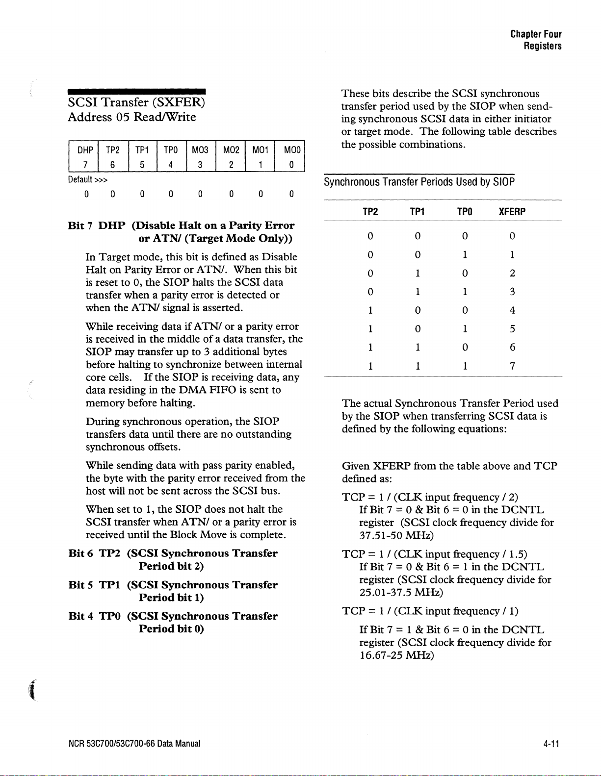
Chapter
Registers
Four
SCSI
Transfer (SXFER)
Address 05 ReadIWrite
M02
DHP
TP2
TP1
TPa
M03
7 6
Default>>>
o a a
Bit 7 DHP
In
Target mode, this bit
on
Halt
is
reset to 0, the
transfer when a parity error
when the A
While receiving data
is
received in the middle
SlOP
before halting to synchronize between internal
core cells.
data residing in the
memory before halting.
During synchronous operation, the
transfers data until there are
synchronous offsets.
5
4 3
o o
(Disable
or A TNI
Parity Error
SlOP
TN/
signal
may transfer
lithe
Halt
on a Parity
(Target
is
defmed
or
ATN/.
halts the
is
is
asserted.
if
A
TN/
of
a data transfer, the
up
to 3 additional bytes
SlOP
is
receiving data, any
DMA
FIFO
no
M01
1 a
2
o a o
Mode
detected
or a parity error
Only»
as
When this bit
SCSI
is
sent to
SlOP
outstanding
MOO
Error
Disable
data
or
These bits describe the SCSI synchronous
SlOP
transfer period used by the
ing synchronous SCSI data in either initiator
or
target mode.
the possible combinations.
Synchronous
Transfer
TP2
0
0 0
0
0
1
1
1 1
1 1
The
actual Synchronous Transfer Period used
by the
defined by the following equations:
SlOP
The
following table describes
Periods
TP1
0 0 0
1
1 1
0 0
0
when transferring
Used
TPO
1 1
0
1
0 6
1
when send-
by
SlOP
XFERP
SCSI
2
3
4
5
7
data
is
(
While sending data with pass parity enabled,
the byte with the parity error received from the
not
be
host will
When set to
SCSI
transfer when A
received until the Block Move
Bit 6 TP2
Bit S TPI
Bit
4 TPO
NCR
53C7aa/53C7aa-66
(SCSI
(SCSI
(SCSI
sent across the
1, the
SlOP
Synchronous
Period
Period
Period
bit
Synchronous
bit
Synchronous
bit
Data
Manual
TN/
2)
1)
0)
SCSI
bus.
does
not
halt the
or a parity error
is
complete.
Transfer
Transfer
Transfer
is
Given
defined as:
TCP
TCP
TCP = 1/
XFERP
=
1/
If
Bit 7 = 0 & Bit 6 = 0 in the
register (SCSI clock frequency divide for
37.51-50
= 1 /
If
Bit 7 = 0 & Bit 6 = 1 in the
register (SCSI clock frequency divide for
25.01-37.5 MHz)
If
Bit 7 = 1 & Bit 6 = 0 in the
register (SCSI clock frequency divide for
16.67 -25
from the table above and
(CLK
(CLK
(CLK
input frequency
MHz)
input frequency / 1.5)
input frequency
MHz)
/2)
DCNTL
DCNTL
/1)
DCNTL
TCP
4-11
Page 48
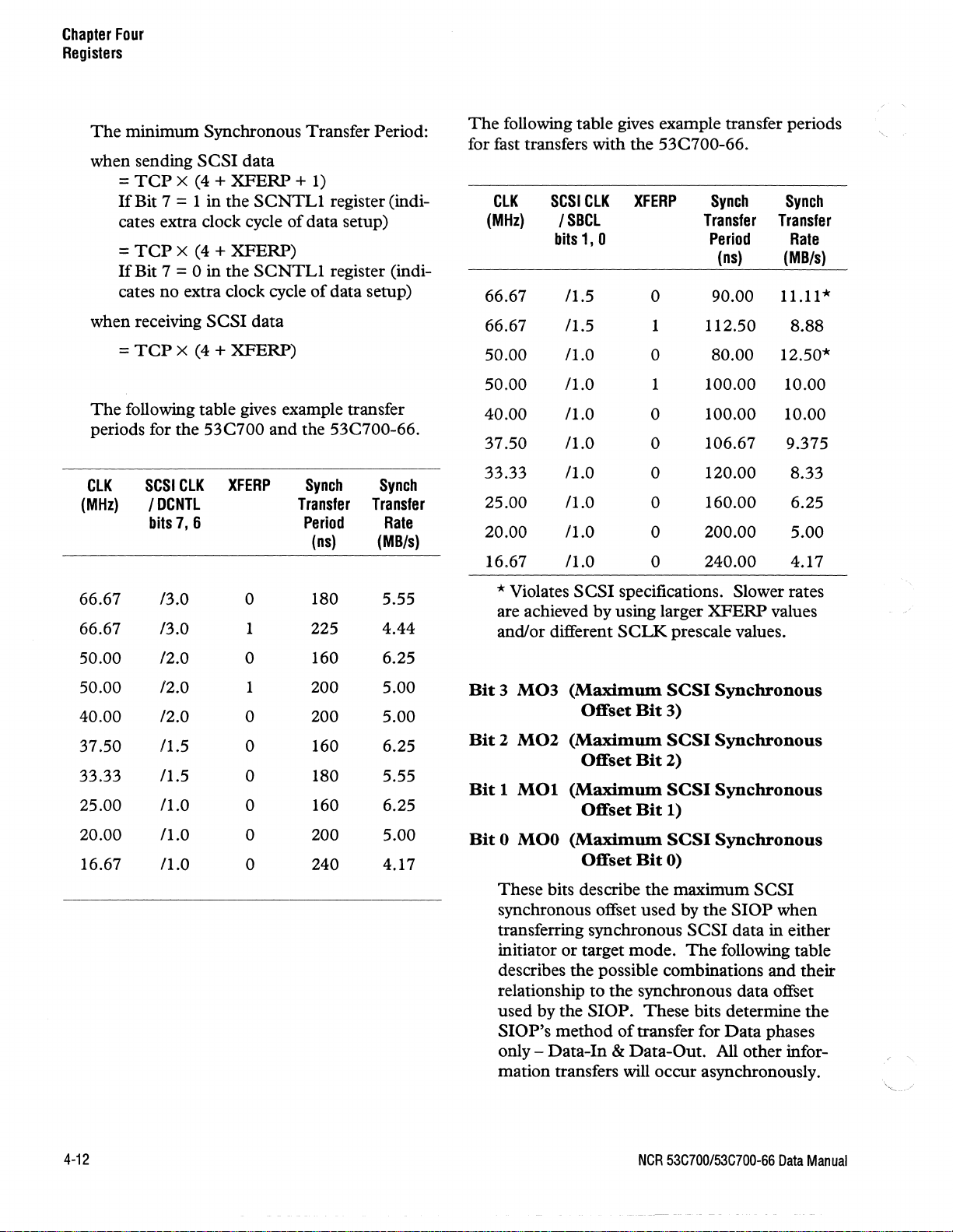
Chapter
Registers
Four
The
minimum Synchronous Transfer Period:
when sending
=TCPX
If
Bit 7 = 1 in the
cates extra clock cycle
=
TCP
If
Bit 7 = 0 in the
cates no extra clock cycle
when receiving
=
TCP
SCSI
data
(4 + XFERP + 1)
SCNTLI
of
x (4 + XFERP)
SCNTLI
SCSI
data
X (4 + XFERP)
register (indi-
data setup)
register (indi-
of
data setup)
The
following table gives example transfer periods
for fast transfers with the
CLK
(MHz)
SCSICLK
/SBCL
bits
1,0
66.67 /1.5
53C700-66.
XFERP
Synch
Transfer
Period
0 90.00
(ns)
66.67 /1.5 1 112.50
50.00
/1.0
0 80.00
Synch
Transfer
Rate
(MB/s)
11.11 *
8.88
12.50*
The
following table gives example transfer
periods for the
CLK
(MHz)
SCSICLK
/DCNTl
bits
53C700
7,6
66.67 /3.0 0
66.67
/3.0
50.00 /2.0 0
50.00 /2.0
and
the 53C700-66.
XFERP
Synch
Transfer Transfer
Period
(ns)
180
1 225 4.44
160
1 200
40.00 /2.0 0 200
37.50
33.33
25.00 /1.0
20.00 /1.0
16.67 /1.0
/1.5 0 160 6.25
/1.5
0 180
0
0
160
200
0 240
Synch
Rate
(MB/s)
5.55
6.25
5.00
5.00
5.55
6.25
5.00
4.17
50.00
/1.0
1 100.00
10.00
40.00 /1.0 0 100.00 10.00
37.50 /1.0 0
33.33
/1.0 0 120.00
25.00 /1.0
20.00 /1.0
16.67 /1.0
* Violates
SCSI
specifications. Slower rates
are achieved by using larger
and/or different
Bit3
M03
Bit 2 M02
Bit 1 MOl
Bit
0 MOO
(Maximum
(Maximum
(Maximum
(Maximum
SCLK
Offset
Offset
Offset
Offset
Bit
Bit
Bit
Bit
0
0
0
106.67
160.00
200.00
240.00
XFERP
prescale values.
SCSI
Synchronous
3)
SCSI
Synchronous
2)
SCSI
Synchronous
1)
SCSI
0)
Synchronous
9.375
values
These bits describe the maximum SCSI
the
SlOP
synchronous offset used by
transferring synchronous
or
initiator
target mode.
SCSI
The
following table
when
data in either
describes the possible combinations and their
relationship to the synchronous data offset
used by the
SlOP's
SlOP.
method
only - Data-In
These bits determine the
of
transfer for
& Data-Out.
Data
All
other infor-
phases
mation transfers will occur asynchronously.
8.33
6.25
5.00
4.17
\,-
"
"
-,/
4-12
NCR
53C700/53C700-66
Data
Manual
Page 49
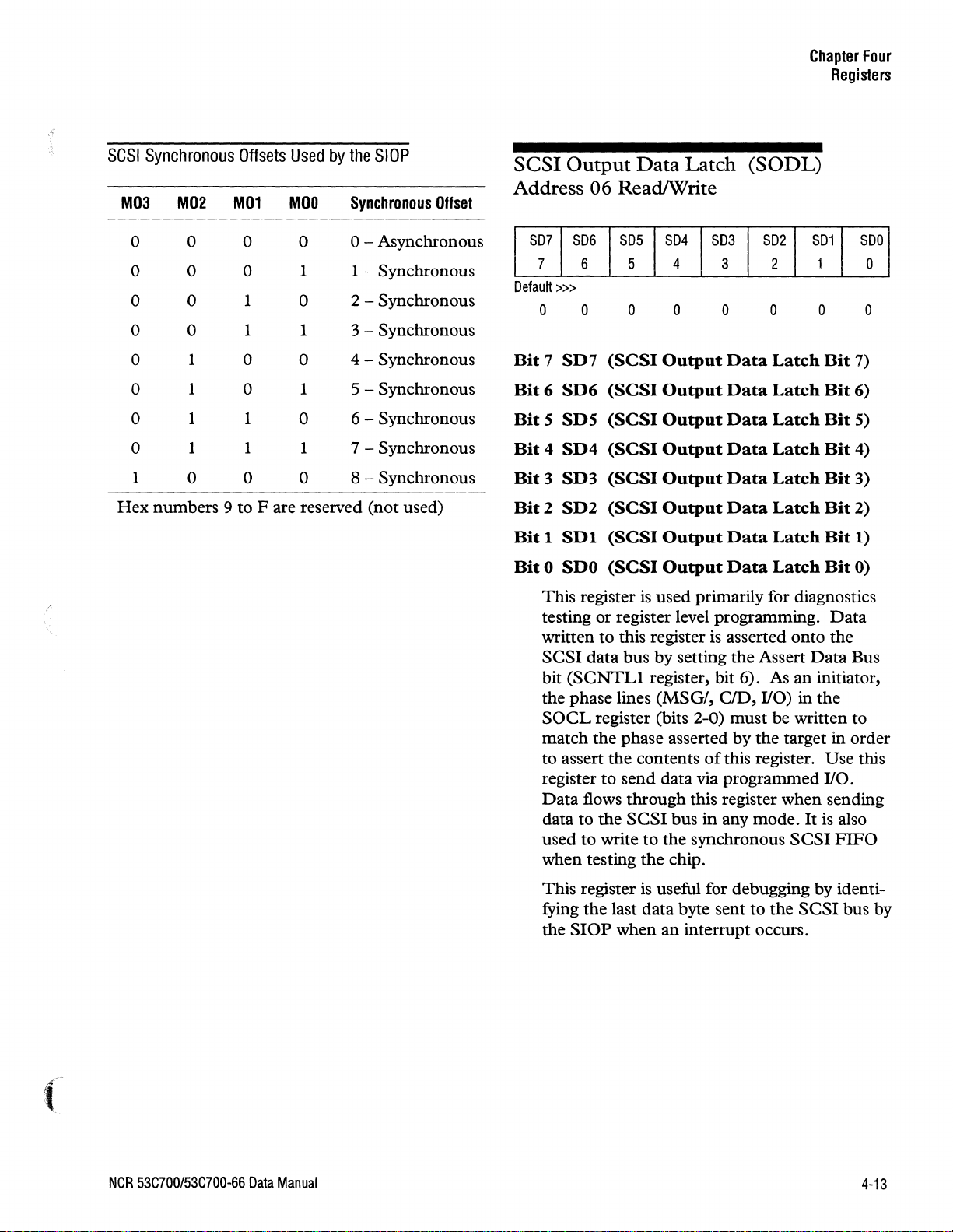
".Ii"
SCSI
Synchronous
M03 M02
Offsets
M01
Used
MOO
by
the
SlOP
Synchronous
Offset
SCSI
Output
Data
Latch (SODL)
Address 06 ReadIWrite
Chapter
Registers
Four
0 0 0
0 0 0
0
0 0
0 1 0 0
0
0 1 1 0 6 - Synchronous
0
1
0
1
1 1 1 7 - Synchronous
0 0
1
1 1 3 - Synchronous
0 1 5 - Synchronous
0
1 1 - Synchronous
0
0 8 - Synchronous
o - Asynchronous
2 - Synchronous
4 - Synchronous
Hex numbers 9 to F are reserved (not used)
S07 S06
7 6
Default
»>
S05
5 4
S04
S03
S02
3 2 1
SD1
o o o o o o o o
Bit 7 SD7
Bit 6 SD6
Bit 5 SDS
Bit 4 SD4
Bit 3 SD3
Bit 2 SD2
Bit 1 SD1
Bit
0 SDO
This register
testing or register level programming.
written to this register
SCSI data bus by setting the Assert
bit
the phase lines
SOCL
match the phase asserted by the target in order
to assert the contents
register to send data via programmed
Data
data to the
used to write to the synchronous
when testing the chip.
(SCSI
(SCSI
(SCSI
(SCSI
(SCSI
(SCSI
(SCSI
(SCSI
Output
Output
Output
Output
Output
Output
Output
Output
is
used primarily for diagnostics
Data
Latch
Data
Latch
Data
Latch
Data
Latch
Data
Latch
Data
Latch
Data
Latch
Data
Latch
is
asserted onto the
Bit
Bit
Bit
Bit
Bit
Bit
Bit
Bit
Data
(SCNTLI
register, bit 6). As an initiator,
(MSG/, CID, I/O) in the
register (bits 2-0) must be written to
ofthis
register. Use this
I/O.
flows through this register when sending
SCSI
bus
in
any mode.
It
is
SCSI
SDO
0
7)
6)
5)
4)
3)
2)
1)
0)
Data
Bus
also
FIFO
(
NCR
53C700/53C700-66
Data
Manual
This register
is
useful for debugging by identifying the last data byte sent to the
the
SlOP
when
an
interrupt occurs.
SCSI
bus by
4-13
Page 50
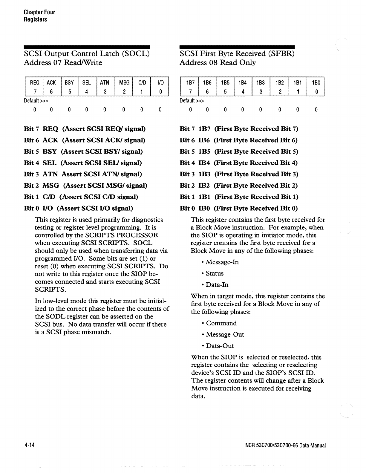
Chapter
Registers
Four
SCSI
Output
Control Latch (SOCL)
Address 07 ReadIWrite
REO
ACK
7 6
Default
>>>
o o o o o o
o
Bit 7 REQ
Bit 6 ACK
Bit S BSY
Bit 4 SEL
Bit 3 ATN
Bit 2 MSG
Bit
1
CID
Bit 0 I/O
This register
(Assert
(Assert
(Assert
(Assert
Assert
(Assert
(Assert
(Assert
SEL
BSY
5
SCSI
is
used primarily for diagnostics
ATN
4 3 2 1
SCSI
SCSI
SCSI
SCSI
SCSI
SCSI
SCSI
I/O
REQI
ACKI
BSYI
SEU
ATNI
MSGI
CID
signal)
MSG
signal)
testing or register level programming. It
controlled by the SCRIPTS PROCESSOR
when executing SCSI SCRIPTS.
should only be used when transferring data via
programmed
(0) when executing SCSI SCRIPTS.
reset
I/O. Some bits are set (1) or
not write to this register once the
comes connected and starts executing
SCRIPTS.
In
low-level mode this register must
ized to the correct phase before the contents
the
SODL
SCSI bus.
is
a SCSI phase mismatch.
register can be asserted on the
No
data transfer
will
C/O
signal)
signal)
signal)
signal)
signal)
signal)
SOCL
SlOP
be
occur
is
be-
SCSI
initial-
if
there
I/O
0
o
Do
SCSI
First Byte Received (SFBR)
Address 08 Read Only
1B7 1B6
7 6 5 4 3 2 1
Default
»>
1B5
o o o o o o
of
Bit 7 IB7
Bit 6 IB6
Bit S IBS
Bit 4 IB4
Bit 3 IB3
Bit 2 IB2
Bit 1 IBl
Bit
0 IBO
This register contains the first byte received for
a Block Move instruction.
the
register contains the
Block Move in any
When in target mode, this register contains the
first byte received for a Block Move in any
the following phases:
(First
(First
(First
(First
(First
(First
(First
(First
SlOP
is
• Message-In
• Status
• Data-In
• Command
• Message-Out
1B4
1B3
1B2
1B1
1BO
o
Byte
Received
Byte
Received
Byte
Received
Byte
Received
Byte
Received
Byte
Received
Byte
Received
Byte
Received
operating in initiator mode, this
first byte received for a
of
the following phases:
Bit
7)
Bit
6)
Bit
S)
Bit
4)
Bit
3)
Bit
2)
Bit
1)
Bit
0)
For
example, when
0
o
of
4-14
• Data-Out
When the
SlOP
is
selected or reselected, this
register contains the selecting or reselecting
SCSI
ID
device's
The
register contents
Move instruction
and the SlOP's SCSI ID.
will
change after a Block
is
executed for receiving
data.
NCR
53C700/53C700-66
Data
Manual
Page 51
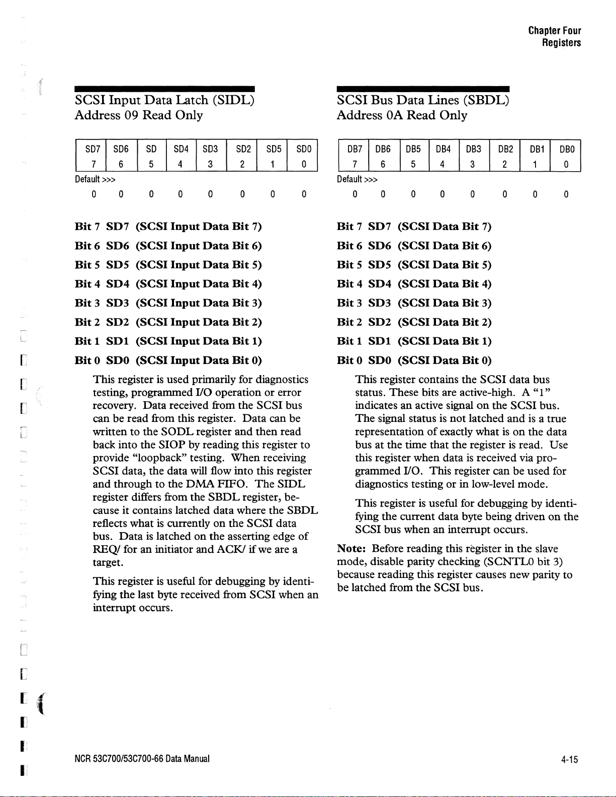
Chapter
Registers
Four
C
L
D
r
L
SCSI
Address
Default
Bit 7 SD7
Bit 6 SD6
Bit 5 SDS
Bit 4 SD4
Bit 3 SD3
Bit 2 SD2
Bit 1 SDI
Bit
Input
Data
Latch (SIDL)
09 Read Only
SD7 SD6
7 6 5 4 3 2
»>
a a
0 SDO
This register
testing, programmed
recovery.
can be read from this register.
written to the
back into the
provide
SCSI
and through to the
register differs from the
cause it contains latched data where the
reflects what
bus.
REQ! for an initiator
target.
This register
fying the last byte received from
interrupt occurs.
so
SD4
S03
SD2
a a o a
(SCSI
(SCSI
(SCSI
(SCSI
(SCSI
(SCSI
(SCSI
(SCSI
"loop back" testing. When receiving
data, the data
Data
Input
Input
Input
Input
Input
Input
Input
Input
is
used primarily for diagnostics
Data
received from the
SODL
SlOP
is
currently
is
latched on the asserting edge
is
useful for debugging by identi-
Data
Bit
Data
Bit
Data
Bit
Data
Bit
Data
Bit
Data
Bit
Data
Bit
Data
Bit
110 operation
Data
register
by reading this register to
will
DMA
and
and
flow into this register
FIFO.
SBDL
register, be-
on
the SCSI data
ACKI
SD5
7)
6)
5)
4)
3)
2)
1)
0)
or
SCSI
then
The
ifwe
SCSI
SDa
1 a
a a
error
bus
can be
read
SIDL
SBDL
of
are a
when an
SCSI
Address
Default
Bit 7 SD7
Bit 6 SD6
Bit 5 SDS
Bit 4 SD4
Bit 3 SD3
Bit 2 SD2
Bit 1 SD1
Bit
Note:
mode, disable parity checking
because reading this register causes new parity to
be
Bus
Data
OA
DB7
DB6
7 6 5 4 3
»>
a
a
0 SDO
This register contains the
status. These bits are active-high.
indicates an active signal
The
signal status
representation
bus at the time that the register
this register when data
grammed
diagnostics testing
This register
fying the current data byte being driven
SCSI bus when an interrupt occurs.
Before reading this register in the slave
latched from the
Lines (SBDL)
Read Only
DB5
DB4
DB3
a
o a
(SCSI
(SCSI
(SCSI
(SCSI
(SCSI
(SCSI
(SCSI
(SCSI
Data
Bit
7)
Data
Bit
6)
Data
Bit
5)
Data
Bit
4)
Data
Bit
3)
Data
Bit
2)
Data
Bit
1)
Data
Bit
0)
SCSI
on
the
is
not latched
of
exactly what
is
received via pro-
110. This register can
or
in low-level mode.
is
useful for debugging by identi-
(SCNTLO bit 3)
SCSI
bus.
DB2
2
a
data bus
A"
SCSI
and
is
on
is
read. Use
be
DB1
DBa
1 a
a a
1 "
bus.
is
a true
the data
used for
on
the
0
[
f]
[)
I:
Ii
(
NCR
53C700/53C700-66
Data
Manual
4-15
Page 52
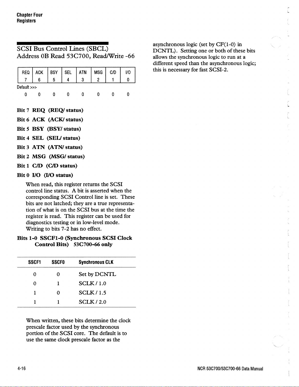
Chapter
Registers
Four
"
L.
SCSI
Address
Default
Bit 7 REQ
Bit 6 ACK
Bit 5 BSY
Bit 4 SEL
Bit 3 ATN
Bit 2 MSG
Bit 1 C/O
Bit 0 I/O
Bus Control Lines (SBCL)
OB
REQ
ACK
7 6 5
»>
o o o o
o
(BSYI
(SEU
(C/D
(I/O
Read
BSY
(REQI
(ACK/
(A
(MSGI
SEL
status)
status)
status)
status)
TNI
status)
status)
status)
53C700,
ATN
4 3
status)
ReadIWrite -66
MSG
c/O
2 1 0
o o
When read, this register returns the SCSI
is
control line status. A bit
corresponding SCSI Control line
asserted when the
is
set. These
bits are not latched; they are a true representa-
is
tion of what
register
is
on the SCSI bus at the time the
read. This register can be used for
diagnostics testing or in low-level mode.
Writing to bits 7-2 has no effect.
110
o
asynchronous logic (set by
DCNTL).
Setting one or both
CF(l-O) in
of
these bits
allows the synchronous logic to run at a
different speed than the asynchronous logic;
is
this
necessary for fast SCSI-2.
,
l
Bits
1-0
SSCF1-0
Control
SSCF1
o
o
1
1
(Synchronous
Bits)
SSCFO
o
1
o
1
53C700-66
Synchronous
Set by
DCNTL
SCLK/l.O
SCLK/l.5
SCLK/2.0
SCSI
only
ClK
When written, these bits determine the clock
prescale factor used by the synchronous
portion
use the same clock prescale factor
4-16
of
the SCSI core.
The
default
as
Clock
is
the
to
NCR
53C700/53C700-66
Data
Manual
Page 53
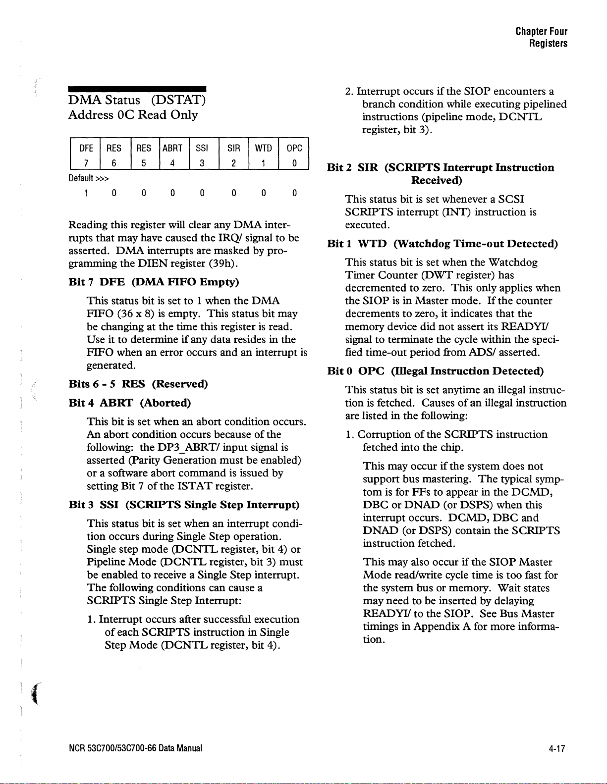
DMA
Status
Address
OC
(DSTAT)
Read
Only
Chapter
2.
Interrupt occurs
branch condition while executing pipelined
instructions (pipeline mode,
register, bit 3).
if
the
SlOP
encounters a
DCNIL
Four
Registers
11·.
DFE
7
Default
RES RES
6
»>
ABRT
5 4 3
a a a a
Reading this register will clear any
that
rupts
asserted.
gramming the
Bit 7 DFE
This
FIFO
be changing at the time this register
Use it to determine
FIFO
generated.
Bits
Bit 4 ABRT
This bit
An abort condition occurs because
following: the
asserted (parity Generation must
or
setting Bit 7
Bit 3 SSI
This status bit
tion occurs during Single Step operation.
Single step
Pipeline
be
The
SCRIPTS
may have caused the
DMA
interrupts are masked by pro-
DffiN
(DMA
status bit
(36 x 8)
when an error occurs and
6 - 5
RES
is
is
(Reserved)
(Aborted)
is
set when an abort condition occurs.
DP3
a software abort command
ofthe
(SCRIPTS
is
mode
Mode
enabled
following conditions can cause a
1. Interrupt occurs after successful execution
of
each
Mode
Step
(DCNIL
to
receive a Single Step interrupt.
Single Step Interrupt:
SCRIPTS
(DCNTLregister,
SSI
SIR
2 1 a
a a a
DMA
IRQ!
register (39h).
FIFO
set
empty.
set when
Empty)
to
1 when the
This
status
if
any data resides in the
an
_
ABRTI
1ST
Single
(DCN'lL
instruction in Single
input signal is
is
issued by
AT
register.
Step
an
interrupt condi-
register, bit 4) or
register, bit 3) must
WTD
signal to be
DMA
interrupt
of
be
Interrupt)
bit 4).
OPC
inter-
bit
may
is
read.
the
enabled)
Bit 2 SIR
is
(SCRIPTS
Interrupt
Instruction
Received)
This status bit
SCRIPTS
executed.
Bit 1 WTD
This status bit
Timer
decremented to zero. This only applies when
the
decrements
memory device did
signal
fied time-out period from
Counter
SlOP
to
Bit 0 OPC
This status bit
tion
is
fetched. Causes
are listed in the following:
1.
Corruption
fetched into the chip.
This
support bus mastering.
tom
is for
DBC
interrupt occurs.
DNAD
instruction fetched.
This
Mode
the system bus
may
READYII
timings in Appendix A for more information.
is
set whenever a
interrupt
(Watchdog
is
in Master mode.
to
terminate the cycle within the speci-
(megal
may occur
FFs
or
DNAD
(or DSPS) contain the
may also occur
read/write cycle time
need
to be inserted by delaying
(!NT)
Time-out
is
set when the Watchdog
(DWT
zero, it indicates
register) has
not
assert its READYII
ADSI
Instruction
is
set anytime
of
of
the
SCRIPTS
if
the system does
to appear in the
(or DSPS) when this
DCMD,
if
or
memory. Wait states
to
the
SlOP.
SCSI
instruction
Detected)
If
the counter
that
the
asserted.
Detected)
an
illegal instruc-
an
illegal instruction
instruction
The
typical symp-
DCMD,
DBC
SCRIPTS
the
SlOP
Master
is
too fast for
See Bus Master
is
not
and
(
NCR
53C700/53C700-66
Data
Manual
4-17
Page 54
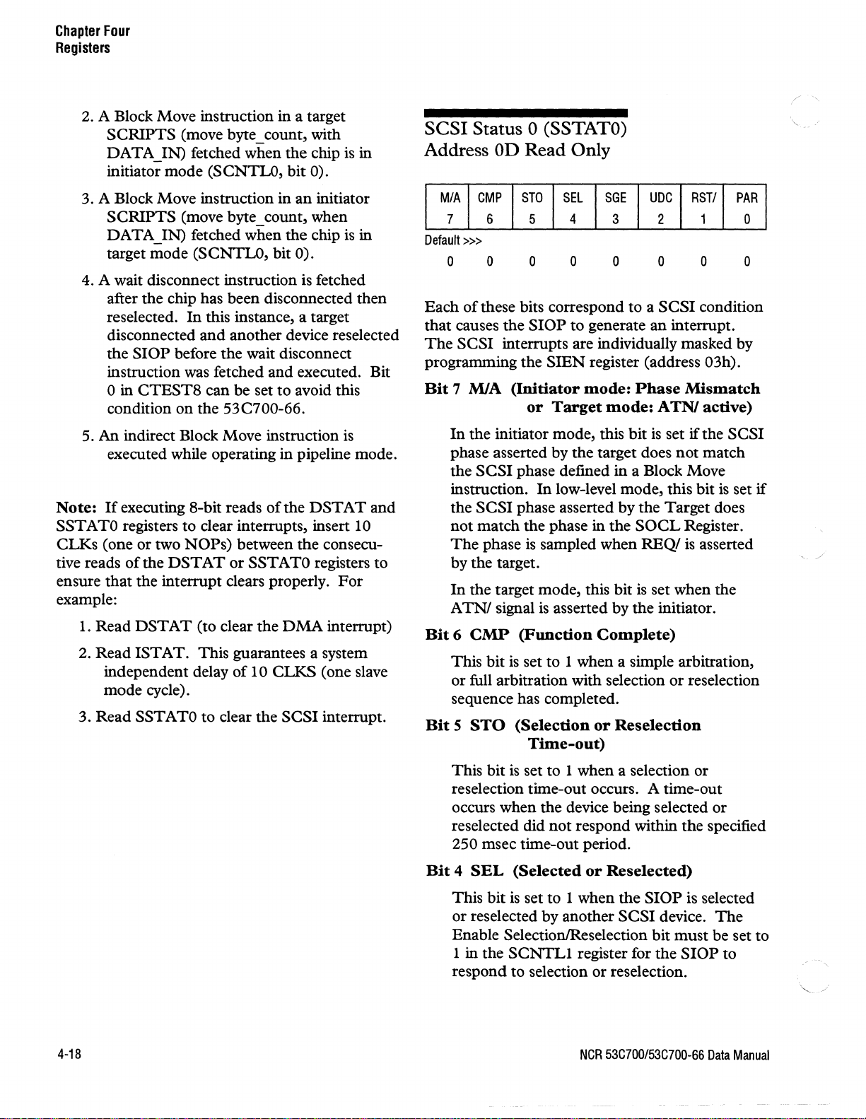
Chapter
Registers
Four
2. A Block Move instruction in a target
SCRIPTS
DATA_IN) fetched when the chip is in
initiator mode (SCNTLO,
3. A Block Move instruction in
SCRIPTS
DATA_IN) fetched when
target mode (SCNTLO, bit
4. A wait disconnect instruction is fetched
after the chip has been disconnected then
reselected.
disconnected
SlOP
the
instruction was fetched and executed. Bit
o in
CTEST8
condition
5. An indirect Block Move instruction is
executed while operating in pipeline mode.
Note:
SST A TO
CLKs
tive reads
ensure
example:
If
executing 8-bit reads
registers
(one
or
of
that
the interrupt clears properly.
1.
Read
DSTAT
Read
2.
3.
ISTAT.
independent delay
mode cycle).
Read
SSTATO
(move byte_count, with
(move byte_count, when
In
this instance, a target
and
another device reselected
before the wait disconnect
two
the
can be set
on
the 53C700-66.
to
clear interrupts, insert 10
Naps)
DSTAT
or
(to clear the
This guarantees a system
of
to
clear
to
of
between the consecu-
SSTATO registers
10
CLKS
the
bit
an
the
0).
avoid this
the
DMA
SCSI
0).
initiator
chip
is
DSTAT
For
interrupt)
(one slave
interrupt.
in
and
to
SCSI
Address
Default
Status 0 (SSTATO)
OD
Read Only
MIA
CMP
7
»>
STO
6
5
SEL
4
SGE
3
o 0 o o o
Each
of
these bits correspond to a
that
causes the
The
SCSI
programming the
Bit
7 MIA
In
the initiator mode, this bit
phase asserted by the target does
the
SCSI
instruction.
the
SCSI
not
match the phase in the
The
phase
by the target.
In
the target mode, this bit
A
TN!
Bit 6 CMP
This
or
full arbitration with selection
sequence has completed.
Bit S STO
SlOP
to
generate
interrupts are individually masked by
SmN
(Initiator
or
phase defined in a Block Move
In
phase asserted by the Target does
is
sampled when REQI
signal
is
(Function
bit
is
set
to
(Selection
register (address 03h).
mode:
Target
low-level mode, this
asserted by the initiator.
mode:
Complete)
1 when a simple arbitration,
or
Time-out)
UDC
RSTI
2 1 0
o o o
SCSI
an
interrupt.
Phase
SOCL
is
Reselection
Mismatch
A TNI active)
is
set
if
not
Register.
is
set when the
or
reselection
PAR
condition
the
SCSI
match
bit
is
set
asserted
if
, /
4-18
This bit
reselection time-out occurs. A time-out
occurs when the device being selected
reselected did
250 msec time-out period.
Bit 4 SEL
This bit
or reselected
Enable SelectionlReselection bit
1 in the
respond to selection
is
set
to
1 when a selection
not
respond within the specified
(Selected
is
set to 1 when the
by
SCNTLI
or
another
register for the
or
NCR
Reselected)
SlOP
SCSI
device.
reselection.
53C700/53C700-66
or
or
is selected
The
must
be set
SlOP
to
Data
to
Manual
.".
/
Page 55
Chapter
Registers
Four
Bit 3 SGE
This bit
SCSI
a
conditions can cause a
condition.
1.
Data
2.
Data
3. Offset Underflow - When the
4.
Offset Overflow - the other
5. Residual data in the synchronous data
(SCSI
is
Gross Error condition.
Underflow - the
was read when no data was present.
Overflow -
written to the
operating in target mode
pulse
is
is
offset
sent a REQ!
which exceeded the maximum synchronous offset defined by the
- a transfer other
receive was started with data left in the
synchronous data
Gross
set to 1 when the
received when the outstanding
zero.
or
Too
SCSI
ACKI
than
FIFO.
Error)
SlOP
SCSI
Gross Error
SCSI
FIFO
many bytes were
FIFO.
and
SCSI
pulse with data
SXFER
synchronous data
encounters
The
following
register
SlOP
an
ACKI
device
is
register.
FIFO
Bit
1
RSTI
(SCSI
This bit
the
Assert
to
multiple interrupts
assertion
Bit 0 PAR
This bit
parity error when sending
data.
the
to become active. A parity error can occur
when receiving data from the
when receiving data from the host bus.
the host bus, parity
ferred from the
register. A parity error can occur from the
host bus only
the SCNTLO register
SCNTLO register
is
SlOP
detects an active
RSTI
1.
This status bit
of
(Parity
is
The
SCNTLO register) must be set for this bit
RSTI
Received)
set to 1 by the following conditions:
RSTI
signal or the
bit in the
the
SCSI
set to 1 when the
Enable Parity Checking bit (bit 3 in
DMA
if
pass parity
SCNTL1
is
edge-triggered so that
do
not
RSTI
Error)
or
is
checked as it
FIFO
register
occur for one
signal.
SlOP
receiving SCSI
SCSI
to the
is
allowed (bit 3 in
= 1, bit 2 in the
= 0).
is
detects a
bus or
From
is
trans-
SODL
set
6. A phase change occurred with an outstanding synchronous offset when the
operating as an initiator.
Bit 2 UDC
When set to 1, the
when a target device unexpectedly disconnects
from the
SlOP
When the
SCRIPTSTM,
disconnect other than a legal SCSI disconnect.
A legal SCSI disconnect can occur after a
Disconnect Message (04h)
Complete Message
message in. A select time-out
at any other time
disconnect. Refer to the SCSI specification
for more detailed information
nects.
nect will cause an interrupt. This interrupt
masked by resetting this bit.
(Unexpected
SCSI
bus. This bit
is
in initiator mode.
SlOP
is
an
unexpected disconnect
is
In
low-level Mode, any type
Disconnect)
IRQI
signal
executing
(OOh)
is
considered an unexpected
is
SCSI
or
received
SlOP
is
asserted
valid when the
a Command
as
or
loss
of
on
SCSI
of
is
is
any
a
busy
discon-
discon-
is
Note:
SST A TO
CLKs (one
tive reads
ensure that the interrupt clears properly.
example:
If
executing 8-bit reads
registers
or
ofthe
1. Read
2.
3. Read SSTATO to clear the
DSTAT
Read
ISTAT.
independent delay
mode cycle).
to
two
NOPs)
DSTAT
clear interrupts, insert
(to clear the
This guarantees a system
of
between the consecu-
or
SSTATO registers to
of
10
the
DSTAT
DMA
CLKS
SCSI
and
10
For
interrupt)
(one slave
interrupt.
(
NCR
53C700/53C700-66
Data
Manual
4-19
Page 56
Chapter
Registers
SCSI Status 1
Address
Default
Bit 7 ILF
Four
(SSTATl)
OE
Read Only
IlF
ORF
7 6 5
>>>
o o
This bit
Latch register
transferred from the
OlF
AlP
o o o o o o
(SIDL
is
Register
set to 1 when the SCSI Input Data
(SIDL) contains data. Data is
lOA
4
3
Full)
WOA
RSTI
2 1 0
SCSI bus to the SCSI
Input Data Latch register before being sent to
the
DMA
SIDL
asynchronously.
does
FIFO
and then to the host bus.
register contains SCSI data received
Synchronous data received
not
flow through this register.
This bit can be used to determine how many
bytes reside in the chip when a
occurs receiving data from
Bit 6 ORF
This bit
Data Register
ter) contains data.
by the
(SODR
is
set to 1 when the SCSI Output
Register
(SODR, a hidden buffer regis-
The
SODR register
SCSI logic
as
a second storage register
when sending data synchronously.
DMA
SCSI.
Full)
It
accessible to the user (cannot be read or
written).
This bit can be used to determine how many
bytes reside in the chip when an error occurs
during a
Bit 5 OLF
SCSI data transfer.
(SODL
Register
Full)
error
is
is
a not
SDP/
The
used
is
mode, data
the
SODL
The
SODR
transferred from the host bus to
register, and then to the SCSI bus.
buffer register
is
not used for
asynchronous transfers.
to
This bit can be used
determine how many
bytes reside in the chip when an error occurs
during data transfer.
Bit 4 AlP
(Arbitration
In
Progress)
Arbitration in Progress (AlP = 1) indicates
that the
tion, asserted
SlOP
has detected a bus free condi-
BSY and asserted its SCSI
onto the SCSI bus.
Bit 3 LOA
Lost Arbitration (LOA =
SlOP
arbitrated for the
tion due to another
SEU
Bit 2 WOA
Won Arbitration (WOA =
SlOP
arbitrated for the
(Lost
Arbitration)
1)
indicates that the
has detected a bus free condition,
SCSI bus, and lost arbitra-
SCSI device asserting the
signal.
(Won
Arbitration)
1)
indicates that the
has detected a bus free condition,
SCSI bus and won arbitra-
tion.
Bit
1
RSTI
(SCSI
RSTI
Signal)
This bit represents the current status
SCSI RST/ signal. This signal
is
not latched
and may be changing when read.
Bit
0
SDPI
(SCSI
SDPI
Parity
Signal)
This bit represents the current status
SCSI
SDP/
parity signal. This signal
and
latched
may be changing when read.
of
of
is
ID
the
the
not
This bit
Data Latch
SODL
DMA
mode, data
the
is
set to 1 when the SCSI Output
(SODL) contains data.
register
is
the interface between the
logic and the SCSI bus.
is
transferred from the host bus to
SODL
register and then to the SCSI
In
Output Data Register (SODR), (a hidden
buffer register which
being sent to the
4-20
is
not accessible), before
SCSI bus. In asynchronous
The
synchronous
NCR
53C700/53C700-66
Data
Manual
Page 57
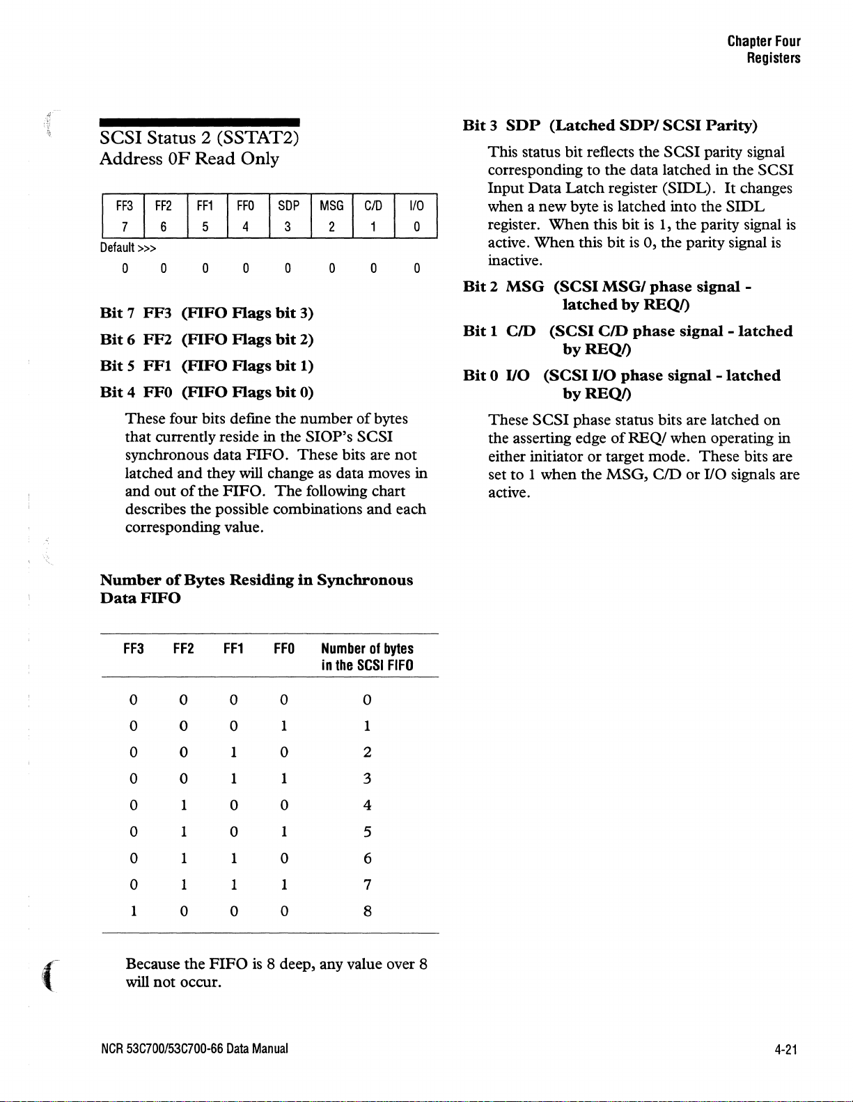
Chapter
Registers
Four
SCSI
Address
Default
Bit
Bit
Bit
Bit
Status 2 (SSTAT2)
OF
Read Only
FF3
FF2
7
>>>
o
7
FF3
6
FF2
5
FFI
4 FFO
These
that
currently reside in the
FF1
6
5 4 3
o o o o
(FIFO
(FIFO
(FIFO
(FIFO
four bits defme the
synchronous data
latched
and
describes
out
and
of
the
the
corresponding value.
FFO
SOP
MSG
c/O
1/0
2 1 0
o o o
Flags
Flags
Flags
Flags
they will change as data moves in
FIFO.
possible combinations
bit
bit
bit
bit
FIFO.
The
3)
2)
1)
0)
number
SlOP's
These
of
bytes
SCSI
bits are
following chart
and
not
each
Bit 3 SDP
(Latched
This status bit reflects the
corresponding
Input
Data
when a
new
register.
active.
When
to
Latch
byte is latched into
When
this bit is 1,
this bit
inactive.
Bit 2 MSG
(SCSI
MSGI
latched
Bit 1 C/D
(SCSI
C/D
byREQI)
Bit 0 I/O
(SCSI
I/O
byREQI)
These
SCSI
phase status bits are latched
the asserting edge
either initiator
set
to
1 when
or
the
active.
SDPI
SCSI
SCSI
the
data latched
register (SIDL).
the
the
parity signal
is
0, the parity signal
phase
by
REQI)
phase
phase
of
REQI
target mode.
MSG,
CID
signal
signal -latched
signal -latched
when operating in
These
or
Parity)
parity signal
in
the
SCSI
It
changes
SIDL
is
is
-
on
bits are
I/O signals are
(
Number
Data
FF3
of
Bytes
Residing
in
FIFO
FF2
0
0 0
0 0 1 0 2
0 0
0
0
0 1 1 0
0 1 1 1 7
1
0
1
1
0 0
Because
will
not
occur.
the
FF1
0 0 0
0
1 1
0
0
FIFO
FFO
1 1
0 4
1
0
is
8 deep, any value over 8
Synchronous
Number
in
the
01
SCSI
bytes
FIFO
3
5
6
8
NCR
53C700/53C700-66
Data
Manual
4-21
Page 58
Chapter
Registers
Four
Scratch A (SCRATCHA)
Address
Default
This
S3C700-66
This
pad
not destroy the contents
ReadlWrites into the
alter its contents. This register can not be accessed by the internal
10-13 ReadIWrite
>>>
all
zeros
register
is
a general purpose user definable scratch
register. Normal
is
chip
available
SCRIPTS
of
SCRA
SCSI
only
in
the
operations will
this register, only slave
TCHA
register will
I/O processor.
Chip Test 0 (CTESTO)
Address 14 Read Only
RES RES RES
7 6 5 4 3
Default
»>
X X
X =
Don't
Care
Bits
7-2
RES
Bit 1 RTRG
This status bit indicates the operating
the logic inside
the status
SCNTLO register.
Mode bit in the SCNTLO register might be
written to
ing in initiator mode. However,
selected as a target, this bit will indicate
the
SlOP
this bit
target,
actually operating
is
idle
status
register.
of
has been selected
is
1, the
and
or
disconnected, this bit
of
the Target
RES
RES
X X
RES
X
(Reserved)
(Real
Target
the
SlOP.
the Target
For
Mode)
It
does
Mode
example, the
° indicating that the
as
SlOP
when this bit
is
actually operating as a
is
0, the
as
an
initiator.
Mode
bit in the SCNTLO
2
X
not
bit in
SlOP
if
a target.
SlOP
If
will
RTRG
DDIR
1
o o
mode
reflect
the
Target
is
operat-
the
SlOP
that
When
is
the
SlOP
reflect the
0
of
is
4-22
Bit 0 DDIR
(Data
Transfer
Direcdon)
This status bit indicates which direction data
being transferred. When this bit
be
will
transferred from
host bus. When this bit
the
is
0,
transferred from the host bus to the
NCR
53C700/53C700-66
is
1, the data
SCSI bus to the
the data will be
SCSI bus.
Data
is
Manual
Page 59
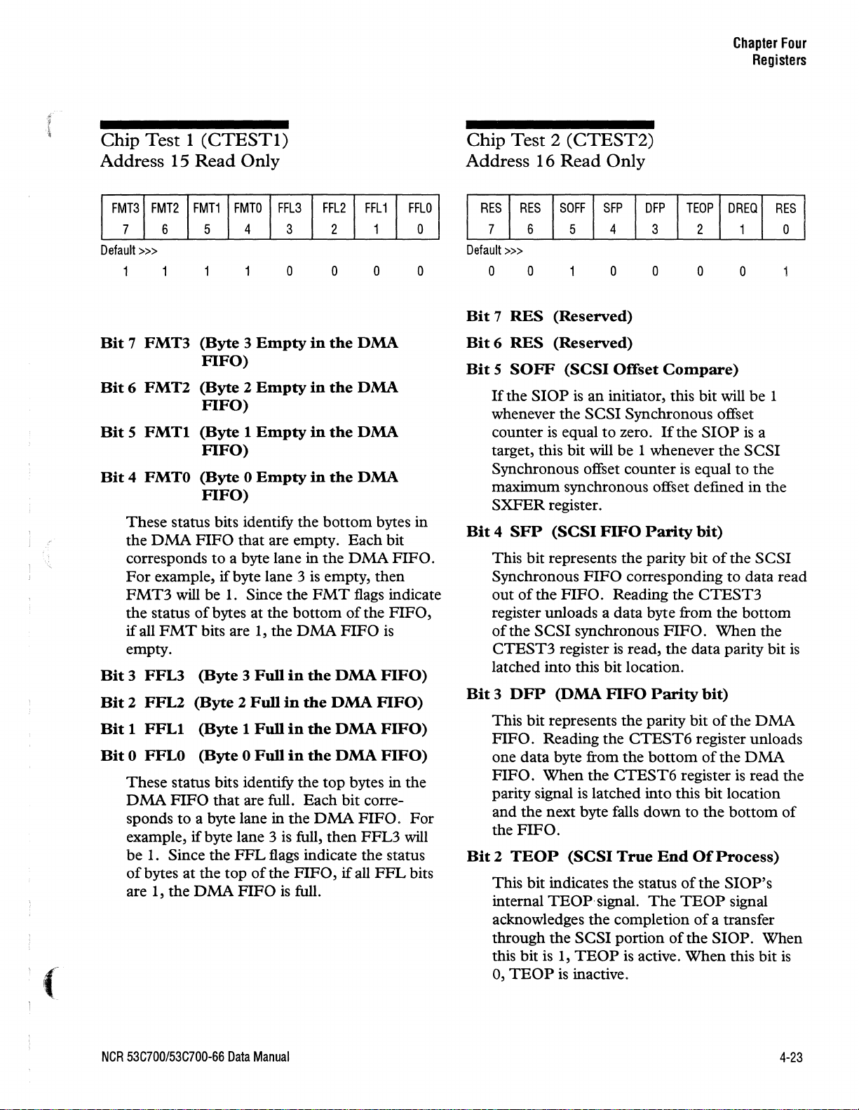
Chapter
Registers
Four
Chip
Address
Default
Bit 7 FMT3
Bit 6 FMT2
Bit 5 FMTI
Bit
1
J
.c
Bit 3 FFL3
Bit 2 FFL2
Bit 1 FFLI
Bit
Test 1 (CTESTl)
15
Read
FMT3 FMT2
7 6 5 4
>>>
4 FMTO
These
the
corresponds
For
FMT3
the
if
all
empty.
0 FFLO
These
DMA
sponds
example,
be
1. Since the
of
bytes at the top
are 1, the
FMT1
(Byte 3 Empty
FIFO)
(Byte 2 Empty
FIFO)
(Byte 1 Empty
FIFO)
(Byte 0 Empty
FIFO)
status bits identify the
DMA
status
FIFO
to
example,
will be 1. Since
FMT
if
of
bytes at the
bits are 1, the
(Byte 3 Full
(Byte 2 Full
(Byte 1 Full
(Byte 0 Full
status bits identify the top bytes in the
FIFO
that
to
a byte lane in the
if
byte lane 3 is full, then
DMA
Only
FMTO
a byte lane in
byte lane 3
FFL
FFL3
that are empty.
are full. Each bit corre-
flags indicate the status
of
the
FIFO
is
3
o
in
in
in
in
is
the
FMT
bottom
DMA
in
the
in
the
in
the
in
the
DMA
FIFO,
full.
FFL2
2 1
o
the
DMA
the
DMA
the
DMA
the
DMA
bottom
Each
the
DMA
empty,
flags indicate
of
the
FIFO
DMA
DMA
DMA
DMA
FIFO.
FFL3
if
all
FFL1
o
bytes in
bit
FIFO.
then
FIFO,
is
FIFO)
FIFO)
FIFO)
FIFO)
FFL
FFLO
0
o
For
will
bits
Chip
Address 16
Default
Bit 7 RES
Bit 6 RES
Bit 5 SOFF
Bit 4 SFP
Bit 3 DFP
Bit 2 TEOP
Test 2 (CTEST2)
Read
RES
RES
SOFF
6
7
»>
o o o
(Reserved)
(Reserved)
If
the
SlOP
whenever the
counter
target, this bit will
Synchronous offset counter is equal
maximum synchronous offset defined
SXFER
This bit represents the parity bit
Synchronous
out
register unloads a
of
CTEST3
latched into this bit location.
This bit represents
FIFO.
one data byte from
FIFO.
parity signal is latched into this bit location
and the next byte falls down to the
the
This bit indicates the status
internal
acknowledges the completion
through
this bit is 1,
0,
is
register.
of
the
the
SCSI
Reading the
When
FIFO.
TEOP'
the
TEOP
equal
(SCSI
FIFO.
register
(DMA
is
Only
SFP
5 4
(SCSI
(SCSI
Offset
is
an
initiator, this bit will
SCSI
Synchronous offset
to
zero.
be
FIFO
FIFO
synchronous
corresponding to data read
Reading the
data
is
read,
FIFO
the
CTEST6
the
the
CTEST6
True
signal.
SCSI
portion
TEOP
inactive.
is active.
DFP
TEOP
3
o
2
o
Compare)
If
the
SlOP
1 whenever
Parity
byte from the
Parity
parity bit
bottom
The
bit)
of
CTEST3
FIFO.
the
data parity bit
bit)
of
register unloads
of
register
End
Of
of
the
TEOP
of
a transfer
of
the
SlOP.
When
the
When
the
Process)
DREQ
1 0
o
be
is
a
SCSI
to
the
in
the
SCSI
bottom
the
the
DMA
DMA
is
read the
bottom
SlOP's
signal
When
this
bit
RES
1
the
is
of
is
(
NCR
53C700/53C700-66
Data
Manual
4-23
Page 60
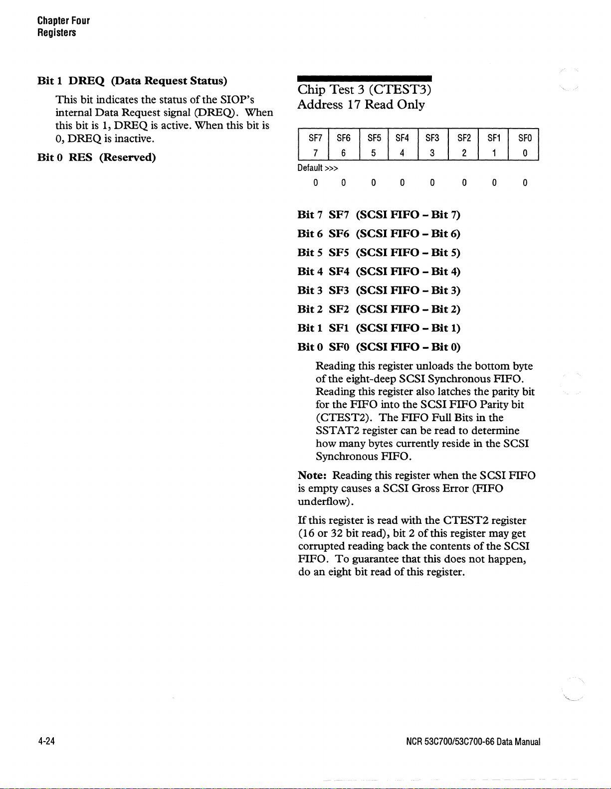
Chapter
Registers
Four
Bit 1 DREQ
(Data
Request
This bit indicates the status
internal
this bit
0,
Bit 0 RES
Data
is
DREQ
Request signal (DREQ). When
1,
DREQ
is
inactive.
(Reserved)
Status)
ofthe
is
active. When this bit
SlOP's
is
Chip Test 3
(CTEST3)
Address 17 Read Only
SF7
SF6 SF5
7 6 5 4 3
Default
>>>
o o o o o
Bit 7 SF7
Bit 6 SF6
Bit
5 SFS
Bit 4 SF4
Bit 3 SF3
Bit 2 SF2
Bit 1 SFI
Bit
0 SFO
Reading this register unloads the bottom byte
of
Reading this register also latches the parity bit
for the
(CTEST2).
SST A T2
how many bytes currently reside in the
Synchronous
(SCSI
(SCSI
(SCSI
(SCSI
(SCSI
(SCSI
(SCSI
(SCSI
the eight-deep
FIFO
register can
SF4
FIFO -Bit
FIFO -Bit
FIFO -Bit
FIFO -Bit
FIFO -Bit
FIFO -Bit
FIFO -Bit
FIFO -Bit
SCSI
into the
The
FIFO
FIFO.
SF3
SF2
2
o
7)
6)
5)
4)
3)
2)
1)
0)
Synchronous
SCSI
FIFO
Full Bits
be
read to determine
Parity bit
in
SF1
1
o o
FIFO.
the
SFO
0
SCSI
4-24
Note:
is
Reading this register when the
empty causes a SCSI Gross
underflow) .
If
this register
or
(16
32 bit read), bit 2
corrupted reading back
FIFO.
do
To
an
eight bit read
is
read with the
the
guarantee that this does
of
this register.
NCR
SCSI
Error
(FIFO
CTEST2
of
this regisler may get
contents
53C700/53C700-66
register
of
the SCSI
not
happen,
FIFO
Data
Manual
Page 61
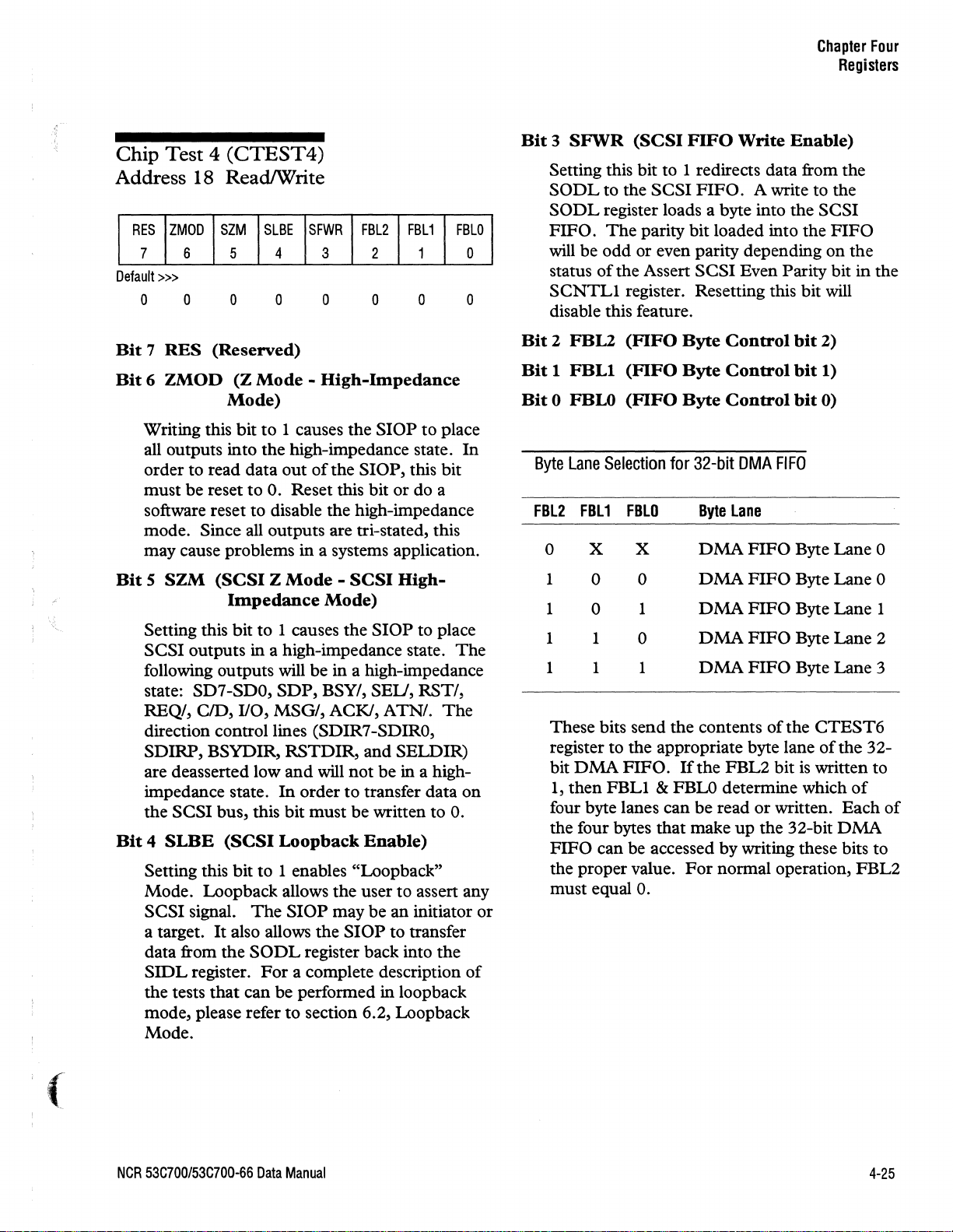
Chapter
Registers
Four
J f
Chip Test 4
(CTEST4)
Address 18 ReadIWrite
RES
ZMOD
7 6 5 4
Default
»>
o o o o o
Bit 7 RES
Bit 6 ZMOD
Writing this bit
all outputs into the high-impedance state.
order to read data out
must be reset
software reset to disable the high-impedance
mode.
may cause problems in a systems application.
Bit S SZM
Setting this bit to 1 causes the
SCSI outputs in a high-impedance state.
following outputs will be in a high-impedance
state:
REQI, CID,
direction control lines (SDIR7-SDIRO,
SDIRP, BSYDIR,
are deasserted low
impedance state.
the SCSI bus, this bit must be written to
Bit 4 SLBE
Setting this bit to 1 enables "Loopback"
Mode. Loopback allows the user to assert any
SCSI signal.
a target.
data from the
SIDL
the tests
mode, please refer to section 6.2, Loopback
Mode.
SZM
SLBE
SFWR
FBL2
FBU
3
2 1
o o o
(Reserved)
(Z
Mode -High-Impedance
Mode)
to
1 causes the
ofthe
to
o.
Reset this bit
Since all outputs are tri-stated, this
(SCSI Z Mode -SCSI
Impedance
SD7-SDO,
110,
SDP,
MSG/,
Mode)
BSY/,
ACKI,
RSTDIR,
and
will
In
order to transfer data
(SCSI
It
also allows the
register.
that
Loopback
The
SlOP
SODL
register back into
For
a complete description
can be performed in loopback
SlOP
to place
SlOP,
this bit
or
do a
High-
SlOP
to place
SEU,
RST/,
ATN/.
and
SELDIR)
not
be
in a high-
Enable)
may be an initiator
SlOP
to transfer
The
o.
the
FBLO
0
In
The
on
or
of
Bit 3 SFWR
(SCSI
FIFO
Write
Enable)
Setting this bit to 1 redirects data from the
SODL
SODL
FIFO.
to the
SCSI
FIFO.
A write to the
register loads a byte into the SCSI
The
parity bit loaded into the
will be odd or even parity depending
status
SCNTLI
the Assert
register. Resetting this bit will
SCSI
Even Parity bit in the
of
disable this feature.
Bit 2 FBL2
Bit 1 FBLI
Bit
0 FBLO
Byte
Lane
FBL2
0
1
1
1 1
I 1 1
These bits send the contents
Selection
FBL1
X X
0 0
0
(FIFO
(FIFO
(FIFO
FBLO
1
0
Byte
Byte
Byte
for
32-bit
Byte
DMA
DMA
DMA
DMA
DMA
Control
Control
Control
DMA
FIFO
Lane
FIFO
FIFO
FIFO
FIFO
FIFO
ofthe
bit
bit
bit
Byte Lane 0
Byte Lane 0
Byte Lane 1
Byte Lane 2
Byte Lane 3
register to the appropriate byte lane
DMA
bit
1,
then
four byte lanes can
the four bytes that make
FIFO
the proper value.
must equal
FIFO.
FBLI
If
the FBL2 bit
is
& FBLO determine which
be
read
or
written. Each
up
the 32-bit
can be accessed by writing these bits to
For
normal operation, FBL2
O.
FIFO
on
the
2)
1)
0)
CTEST6
of
the 32-
written to
of
DMA
of
(
NCR
53C700/53C700-66
Data
Manual
4-25
Page 62
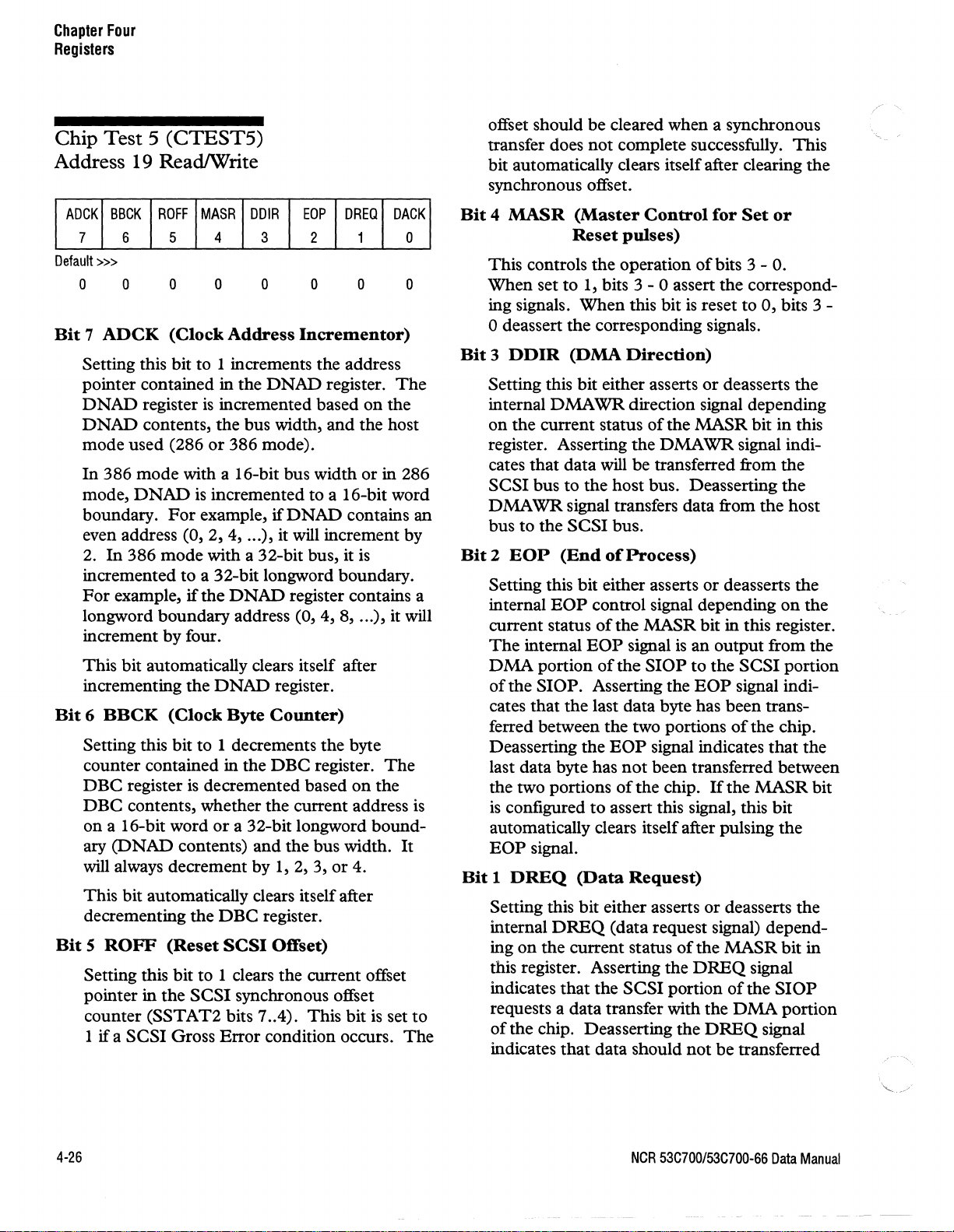
Chapter
Registers
Four
Chip
Test 5 (CTEST5)
Address 19 ReadIWrite
BBCK
ADCK
7 6 5 4
Default
»>
o o o
Bit 7 ADCK
Setting this bit to 1 increments the address
pointer contained in the
DNAD
DNAD
mode used (286
In
386 mode with a 16-bit bus width or in 286
mode,
boundary.
even address
2.
In
incremented to a 32-bit longword boundary.
For
longword boundary address
increment by four.
This bit automatically clears itself after
incrementing the
Bit 6 BBCK
Setting this bit to 1 decrements the byte
counter contained in the
DBC
DBC
on a 16-bit word
ary (DNAD contents) and the bus width.
will
This bit automatically clears itself after
decrementing the
Bit S ROFF
Setting this bit to 1 clears the current offset
pointer in the
counter
1 if a
ROFF
MASR
DDIR
3
o o
(Clock
register
contents, the bus width, and the host
DNAD
For
386 mode with a 32-bit bus, it
example,
(Clock
register
contents, whether the current address
always decrement by 1, 2, 3, or 4.
(Reset
(SSTAT2 bits 7 .. 4). This bit
SCSI Gross Error condition occurs.
Address
DNAD
is
incremented based on the
or
386 mode).
is
incremented to a 16-bit word
example,
(0, 2, 4, ...
if
the
DNAD
is
decremented based
or
DBC
SCSI
SCSI
ifDNAD
),
it will increment by
DNAD
Byte
a 32-bit longword bound-
register contains a
(0,4,8,
register.
Counter)
DBC
register.
Offset)
synchronous offset
DREQ
EOP
2 1 0
o o o
Incrementor)
register.
contains an
register.
is
...
on
),
The
the
is
set to
it will
DACK
The
is
It
The
offset should be cleared when a synchronous
transfer does not complete successfully. This
bit automatically clears itself after clearing the
synchronous offset.
Bit 4 MASR
This controls the operation
When set to 1, bits 3 - ° assert the correspond-
ing signals. When this bit
(Master
Reset
pulses)
Control
of
is
for
Set
bits 3 - 0.
reset to 0, bits 3 -
° deassert the corresponding signals.
Bit 3 DDIR
Setting this bit either asserts or deasserts the
internal
on
the current status
register. Asserting the DMAWR signal indicates that data
SCSI bus to the host bus. Deasserting the
DMA
bus to the
Bit 2 EOP
Setting this bit either asserts
internal
current status
The
DMA
of
the SlOP. Asserting the
cates that the last data byte has been transferred between the two portions
Deasserting the
last data byte has
the two portions
is
configured to assert this signal, this bit
automatically clears itself after pulsing the
EOP
Bit 1 DREQ
Setting this bit either asserts or deasserts the
internal
on
ing
this register. Asserting the
indicates that the
requests a data transfer with the
of
the chip. Deasserting the
indicates that data should
(DMA
DMA
WR
signal transfers data from the host
SCSI bus.
(End
EOP
internal
portion
signal.
(Data
DREQ
the current status
Direction)
WR
direction signal depending
of
the MASR bit in this
will
be transferred from the
of
Process)
or
deasserts the
control signal depending
of
the MASR bit in this register.
EOP
of
EOP
signal
the
not
ofthe
is
an output from the
SlOP
to
the SCSI portion
EOP
signal indicates that the
been transferred between
chip.
If
the MASR bit
Request)
(data request signal) depend-
of
the MASR bit in
DREQ
SCSI
portion
DREQ
not
be transferred
signal indi-
of
the chip.
signal
of
the
DMA
signal
or
on
the
SlOP
portion
4-26
NCR
53C700/53C700-66
Data
Manual
Page 63
Chapter
Registers
Four
between the SCSI portion
DMA
portion.
If
the MASR bit
ofthe
SlOP
is
configured
to assert this signal, this bit automatically
clears itself after asserting the
Bit 0 DACK
(Data
Acknowledge)
Setting this bit either asserts
internal
on
DACKI
the current status
data request signal dependent
register. Asserting the
that the
DMA
portion
edges a data transfer with the
the chip. Deasserting the
DREQ
or
of
the MASR bit in this
DACKI
of
the
SlOP
SCSI
DACKI
signal.
deasserts the
signal indicates
acknowl-
portion
signal
indicates that data should not be transferred
between the
DMA
the SCSI portion.
portion
If
of
the MASR bit
the
SlOP
is
ured to assert this signal, this bit automatically
clears itself after asserting the
DACKI
and the
and
config-
signal.
of
Chip
Address
Default
Test 6 (CTEST6)
lA
ReadIWrite
DF7
DF6 DF5
7 6
>>>
5 4 3
DF4
DF3 DF2
2
o 0 o o o o
Bit 7 DF7
Bit 6 DF6
Bit 5 DF5
Bit 4 DF4
Bit 3 DF3
Bit 2 DF2
Bit 1 DF1
Bit
0 DFO
A write to this register writes data to the
appropriate byte lane
determined by the
register. Reading this register unloads data
from the appropriate byte lane
FIFO
CTEST4
loaded into the top
out
is
read from the
that byte
FIFO
(DMA
(DMA
(DMA
(DMA
(DMA
(DMA
(DMA
(DMA
as
determined by the
register.
of
the
FIFO
is
latched and stored in the
parity bit in the
FIFO -Bit
FIFO -Bit
FIFO -Bit
FIFO -Bit
FIFO -Bit
FIFO -Bit
FIFO -Bit
FIFO -Bit
of
FBL
Data
ofthe
7)
6)
5)
4)
3)
2)
1)
0)
the
DMA
bits in the
of
the
FBL
bits in the
written to the
FIFO.
Data
from the bottom. When data
DMA
FIFO,
the parity bit for
CTEST2
register.
DF1
DFO
1
o o
FIFO
as
CTEST4
DMA
FIFO
is
read
DMA
0
is
NCR
53C700/53C700-66
Data
Manual
Do
not
read
starting
DMA
or
FIFO
SCRIPTS
FIFO
the
or
write to this register before
restarting a
is
not
SCSI
SCRIPTS.
If
the
cleared before executing a
Block Move instruction, data left in
will be transferred.
4-27
Page 64
Chapter
Registers
Four
Chip Test 7
Address
RES
RES
7 6 5 4 3 2 1 0
Default
>>>
o o o
Bit 7 RES
Bit 6 RES
Bit 5 RES
Bit 5 FM
(CTEST7)
IB
ReadIWrite
FM
(Reserved)
(Reserved)
(Reserved)
(Fetch
STD
DFP
o o o
53C700
Mode)
53C700-66
EVP
only
DC
o o
only
This bit, in conjunction with the Fetch/Master
enable bit
will
modify the function
of
the
Fetch output. When the Fetch/Master enable
is
set and this bit
is
set, the Fetch! pin
deassert during indirect read operations.
will
Fetch/
portion
not
become active until the Fetch/Master
enable
only be active during the opcode
of
an instruction fetch. This bit
is
asserted, causing the read back
capability to be disabled.
will
will
DIFF
Bit 2 EVP
Setting this bit to 1 causes the
(Even
Parity)
SlOP
to gener-
ate even parity when sending data to the host
It
bus.
parity
bit
will also check the host bus for even
if
parity checking
3).
Setting this bit to ° causes odd parity
is
enabled (SCNTLO,
to be generated on the host side.
Bit 1 DC
Setting this bit to 1 causes the
the
(DCI
Output
Instruction
Signal
Fetches)
Low
SlOP
DCI
signal low when fetching SCRIPTS
For
to drive
instructions from memory. This allows the
user the option
a cache or forcing
of
memory. However, the
become valid until
ceived and the
of
storing
them
HOlDA!
SlOP
SlOP
to
instructions in
be read directly out
DCI
signal does
has been re-
has started the first bus
master cycle.
When this bit
driven high.
reset to
The
DC!
0,
the
signal
DC!
signal
is
always driven
is
high when moving data tolfrom memory and
can only be driven low during instruction fetch
cycles.
Bit 0 DIFF
(Differential
Mode)
not
is
Bit 4 STD
(Selection
Time-out
Disable
This bit disables the selection time-out timer.
or
A selection
reported when this bit
Bit 3 DFP
reselection time-out
is
(DMA
FIFO
Parity
This bit represents the parity bit
FIFO
FIFO
when reading data out
via programmed 110 (CTEST6).
order to transfer data tolfrom the
perform a read or a write to the
set.
will
bit)
ofthe
of
the
DMA
CTEST6
DMA
register. When loading data into the
write this bit to the
FIFO
as the parity bit for
each byte loaded. Set this bit with the status
of
the parity bit to be written to the
before writing the byte to the
details
DMA
DMA
of
performing a diagnostic test
FIFO,
FIFO
please refer to the Diagnostics
Test
section
of
this manual.
FIFO.
FIFO
Bit)
not
DMA
In
FIFO,
FIFO,
For
of
the
be
Setting this bit to 1 enables the
SlOP
to
interface with external differential pair trans-
ceivers.
and
For
the two modes, refer
The
function
RST/,
is
different for differential mode.
more information
of
the SCSI
on
differences between
to
the pin descriptions for
BSY/,
SEU
these signals in Chapter 3. Resetting this bit
enables single-ended mode. This bit should
if
be set to 1 during initialization
is
tial pair interface
to be used.
the differen-
4-28
NCR
53C700/53C700-66
Data
Manual
Page 65
Chapter
l
'\
Temporary Stack
Address 1
C-IF
(TEMP)
ReadIWrite
DMA
FIFO
(DFIFO)
Address 20 ReadIWrite
Four
Registers
Default
»>
all
zeros
This 32-bit register stores the instruction address
pointer for a
in this register
upon
execution
points
not write to the
executing SCSI SCRIPTS.
CALL.
is
to
the next instruction to be executed.
The
address pointer stored
loaded into the
ofa
RETURN.
TEMP
register while the
DSP
register
This address
Do
SlOP
is
FlF
7 6 5
Default
>>>
o
The
8-bit reads or writes. A 16- or 32-bit read or
write
ISTAT
any internal bus contentions while executing
SCRIPTS, any other registers accessed during
a read
disabled
Bit 7 FLF
When set to 1, data residing in the
FIFO
address in the
SlOP
(DSTAT, bit 7 equals one), this bit should be
written to
Bit 6 CLF
B05
elF
o o
DFIFO
of
this register would also include the
register.
or
a write
and
(Flush
is
transferred to memory starting at the
has successfully transferred the data
B04
B03
4
o o
register can only be accessed by
To
protect the
of
the 1ST A T register
appear
as
DMA
DNAD
FF.
FIFO)
register. Once the
B02
B01
3
2
o
SlOP
1 0
o o
DMA
o.
(Clear
DMA
and
SCSI
FIFOs)
BOO
from
will
be
(
When set to 1, the SCSI and
pointers are cleared.
SODL,
register are reset to
resets to
cleared the appropriate
registers .
Bits
5-0
These six bits indicate the amount
transferred between the
DMA
bytes in the
These bits
between the two cores.
stopped transferring data, these bits are stable.
and
SODRfull
0 after the
B05-0
core. Use it to determine the number
(Bits
DMA
will
In
o.
This bit automatically
SlOP
5-0
Counter)
FIFO
change when data
DMA
addition, the SIDL,
bits in the
has successfully
FIFO
FIFO
SCSI core and the
when an error occurs.
Once the chip has
FIFO
SSTATI
pointers and
Byte
Offset
of
is
transferred
data
of
NCR
53C700/53C700-66
Data
Manual
4-29
Page 66
Chapter
Registers
Four
Data
rupt
may
occurs
remain in
in
Move instruction.
stance is a disconnect
middle
many
the
When
1.
of
a block move.
bytes reside in
following steps:
sending
Read
this
DFIFO
the
middle
SCSI
the
chip when
of a SCRIPTS
The
most
by
a target device in
To
the
DMA
data,
register
an
inter-
Block
common
circum-
the
determine how
FIFO,
perform
If
a
SCSI
interrupt occurs
the
data,
transferred
no
however, a
data left in the
bytes left
to
host memory.
to
recover in
DMA
Interrupt) occurs
on
the
host
side,
continue
there
may
the
data
be
bytes remaining in
when
receiving
DMA
interrupt
or
some catastrophic error
and
the
transfer
the
(DMA
chip
to
FIFO
There
FIFO.
is
unable
host
memory,
should be
Watchdog
the
will
If,
to
FIFO.
be
2. Mask the
hex
3.
Read
the
4.
Mask
the
hex
5.
Subtract
the
from
6.
7.
Mask
The
any carry bits by
3F
with
final result will
bytes
When
1.
2.
receiving
Read
Mask
the
the
hex
3.
Read
the
4.
Mask
the
hex
upper
2 bits by
lower 8 bits
upper
the
2 bits by
6-bit value
6-bit value
hex
SCSI
lower 8 bits
upper
DFIFO
upper
2 bits by
register
2 bits by
of
the
of
of
the
ANDing
be
between 0
data,
ofthe
ANDing
DBC
ANDing
the
DBC
DFIFO
the
DBC
ANDing
ANDing
with
3F
register
with
3F
register
register
result
and
32
register
with
3F
with
3F
4-30
5.
Subtract
register from
register
Mask
6.
with
7.
The
final result will
bytes
the
6-bit value
the
6-bit value
any carry bits by
3Fhex
be
of
the
DFIFO
ofthe
ANDing
between 0
the
and
DBC
result
32
NCR
53C700/53C700-66
Data
Manual
Page 67
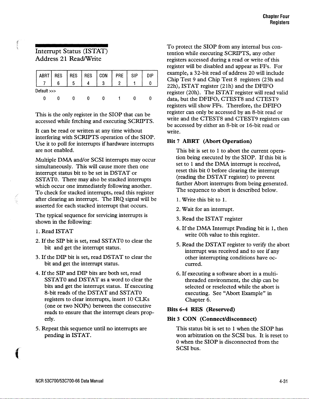
Interrupt Status (ISTAT)
21
Address
ABRT
7
Default
>>>
o
This
is
the only register in the
accessed while fetching and executing SCRIPTS.
It
can be read
interfering with
it to poll for interrupts
Use
not
are
Multiple
simultaneously. This will cause more then one
interrupt status bit to be set in
SSTA
which occur one immediately following another.
To
after clearing an interrupt.
asserted for each stacked interrupt that occurs.
The
shown in the following:
1. Read
2.
3.
enabled.
TO.
check for stacked interrupts, read this register
typical sequence for servicing interrupts
If
the
bit and get the interrupt status.
If
the
bit and get the interrupt status.
ReadIWrite
RES
RES RES
6 5 4 3 2 1 0
o
o o o o o
or
written at any time without
SCRIPTS
DMA
ISTAT
SIP
DIP
and/or SCSI interrupts may occur
There may also be stacked interrupts
bit
is
set, read SSTATO to clear the
bit
is
set, read
CON
operation
PRE
SlOP
if
hardware interrupts
DSTA T or
The
IRQ
DSTAT
SIP
that can
of
the SlOP.
signal will be
to clear the
DIP
be
is
Chapter
Registers
To
protect the
tention while executing
registers accessed during a read or write
register
example, a 32-bit read
Chip
22h),
register (20h).
data, but the
registers will show
register can only be accessed by an 8-bit read or
write and the
be accessed by either an 8-bit
write.
Bit 7 ABRT
will
Test 9 and
ISTAT
This bit
tion being executed by the
set to 1
reset this bit
(reading the
further Abort interrupts from being generated.
The
sequence to abort
1.
Write this bit to 1.
2. Wait for
3. Read the
4.
If
the
write
5. Read the
interrupt was received and to see
other interrupting conditions have occurred.
SlOP
from any internal bus con-
SCRIPTS,
be
disabled and appear
of
address 20 will include
Chip
Test
8 registers (23h and
register (21h)
The
ISTAT
DFIFO,
FFs.
CTEST8
(Abort
is
set to 1 to abort the current opera-
and
the
DMA
0 before clearing the interrupt
DSTAT
an
interrupt.
ISTAT
DMA
Interrupt Pending bit
OOh
value
DSTAT
and
register
CTEST8
Therefore, the
and
CTEST9
Operation)
interrupt
register) to prevent
is
described below.
register
to
this register.
register to verify the abort
any other
as
the
DFIFO
will
and
or
16-bit read
SlOP.
is
of
FFs.
read valid
CTEST9
DFIFO
registers can
If
this bit
received,
is
if
this
For
or
1,
any
then
Four
is
(
4.
Ifthe
SIP
and
DIP
bits are both set, read
SSTATO
bits and get the interrupt status.
8-bit reads
registers to clear interrupts, insert 10 CLKs
(one
reads to ensure that the interrupt clears properly.
5. Repeat this sequence until no interrupts are
pending in
NCR
53C700/53C700-66
or
and
two
DSTAT
of
the
Naps)
1ST
AT
Data
as a word to clear the
If
executing
DSTAT
between the consecutive
.
Manual
and
SSTATO
If
executing a software abort in a multi-
6.
threaded environment, the chip can be
selected
executing. See "Abort Example" in
Chapter 6.
Bits
6-4
RES
Bit 3 CON
This status bit
won arbitration
o when the
SCSI bus.
or
reselected while the abort
(Reserved)
(Connect/disconnect)
is
set to 1 when the
on
the
SCSI
bus.
SlOP
is
disconnected from the
SlOP
It
is
reset to
is
has
4-31
Page 68
Chapter
Registers
Four
This bit
is
automatically set anytime the
becomes connected as an initiator or a target.
is
Connected
on the SCSI bus
defined by winning arbitration
or
when the
SlOP
has re-
sponded to a selection or reselection.
SlOP
4. Watchdog timer counter decremented
zero, indicating that a host memory time-
out occurred
5. Illegal
SCRIPTS
instruction detected
/-
to
Bit 2 PRE
This status bit
DSP
(Pointer
is
set
Register
to
1 when the
registers are empty.
Empty)
In
pipeline mode,
poll this register to determine when the
is
ready to accept another instruction. This bit
is
always set unless using pipeline mode.
Bit 1 SIP
This status bit
condition
the SlOP.
(SCSI
Interrupt
is
set
is
detected in the SCSI portion
To
determine which condition(s)
Pending)
to
1 when an interrupt
have occurred, read the SSTATO register.
indicates that one
of
the following SCSI
interrupt conditions has occurred.
1.
Phase Mismatch (Initiator Mode) or
active (Target Mode)
2. Function Complete
or
3. Selection
The
4.
5.
SlOP
SCSI
Gross Error occurred
Reselection Time-out occurred
was selected
or
reselected
DSPS
SlOP
ATNI
and
of
It
Note:
SST A TO
two
reads
If
executing 8-bit reads
of
the
DST
registers to clear interrupts, insert one or
Naps
(10 CLKs) between the consecutive
of
the
DSTA
T or SSTATO registers to
ensure that the interrupt clears properly.
example:
1.
Read
DSTAT
2. Read 1ST
(to
clear the
AT
(10 CLKs for one slave mode,
DMA
interrupt)
register read cycle)
3. Read SSTATO to clear the SCSI interrupt.
AT
For
and
6.
Unexpected Disconnect occurred
SCSI
7.
8.
Bit 0 DIP
This status bit
condition
the SlOP.
have occurred, read the
indicates that one
Reset detected active
Parity Error received
(DMA
Interrupt
is
set to 1 when an interrupt
is
detected
To
determine which condition(s)
in
of
the following
the
DSTAT
interrupt conditions has occurred.
1.
Abort condition detected
SCRIPTS
2.
SCSI
3.
single step interrupt received
SCRIPTS
Interrupt instruction
Pending)
DMA
portion
register.
DMA
of
It
4-32
NCR
53C700/53C700-66
Data
Manual
Page 69
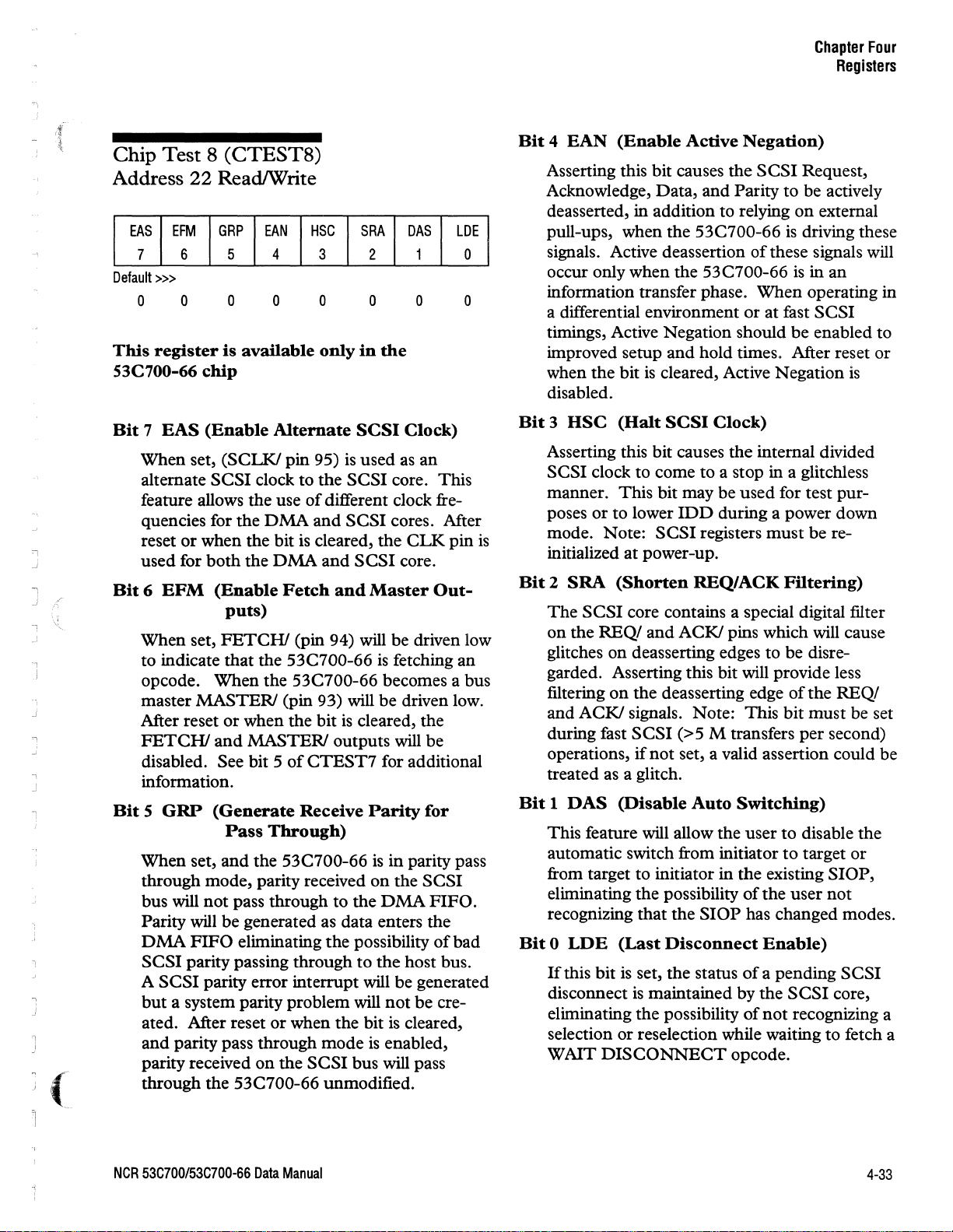
Chapter
Registers
Four
'1
J
]
J
,
J
1
,f
~.
Chip Test 8
(CTEST8)
Address 22 ReadIWrite
EFM
GRP
EAN
EAS
7 6
Default
>>>
5 4 3
o o o o o
This
register
S3C700-66
Bit 7 EAS
When set,
alternate SCSI clock to the
feature allows the use
quencies for the
reset
used for
Bit 6 EFM
When set,
to indicate that the
opcode. When the
master MASTERJ (pin 93) will be driven low.
After reset
FETCH!
disabled. See bit 5
information.
Bit S GRP
When set,
through mode, parity received
bus will not pass through to the
Parity will
DMA
SCSI parity passing through to the host bus.
SCSI
A
but
a system parity problem will
ated. After reset
and
parity pass through mode
parity received
through the
is
available
chip
(Enable
(SCLKI
or
when the bit
both
the
(Enable
puts)
FETCH!
or
when the bit
and
MASTERJ outputs will be
(Generate
Pass
and
the 53C700-66
be
generated as data enters the
FIFO
eliminating
parity error interrupt will
on
53C700-66 unmodified.
HSC
SRA
2
DAS
o
only
in
the
Alternate
pin 95)
of
DMA
is
DMA
Fetch
(pin 94) will be driven low
53C700-66
53C700-66 becomes a bus
of
CTEST7
Receive
Through)
or
when the bit
the
SCSI
SCSI
is
SCSI
Clock)
used as an
core. This
different clock fre-
and
SCSI
cores. After
cleared, the
and
SCSI
and
is
cleared, the
CLK
core.
Master
is
fetching an
for additional
Parity
is
in
parity pass
on
the
DMA
the
possibility
be
not
be
is
cleared,
is
enabled,
bus will pass
LDE
1 0
o o
pin
is
Out-
for
SCSI
FIFO.
of
bad
generated
cre-
Bit 4 EAN
Asserting this bit causes the
(Enable
Active
Negation)
SCSI
Request,
Acknowledge, Data, and Parity to be actively
on
deasserted, in addition to relying
pull-ups, when the
signals. Active deassertion
occur only when the
information transfer phase.
a differential environment
53C700-66
of
these signals will
53C700-66
When
or
at fast
external
is
driving these
is
in an
operating in
SCSI
timings, Active Negation should be enabled to
improved setup and hold times. After reset or
is
when the bit
cleared, Active Negation
disabled.
Bit 3 HSC
(Halt
SCSI
Clock)
Asserting this bit causes the internal divided
SCSI clock to come to a stop in a glitchless
manner. This bit may be used for test pur-
or
poses
mode. Note:
initialized
Bit 2 SRA
The
SCSI
on
the REQI
glitches
to lower
at
(Shorten
core contains a special digital fIlter
on
IDD
during a power down
SCSI
registers
must
be re-
power-up.
and
ACKI
REQlACK
pins which will cause
Filtering)
deasserting edges to be disregarded. Asserting this bit will provide less
fIltering
and
during fast
operations,
on
ACKI
the deasserting edge
of
signals. Note: This bit
SCSI
(>5 M transfers
if
not
set, a valid assertion could be
the REQI
must
per
treated as a glitch.
Bit 1 DAS
(Disable
Auto
Switching)
This feature will allow the user to disable the
to
automatic switch from initiator
target
from target to initiator in the existing
eliminating the possibility
recognizing that the
Bit 0 LDE
If
this bit
disconnect
(Last
Disconnect
is
set, the status
is
maintained by the
eliminating the possibility
or
selection
WAIT
reselection while waiting to fetch a
DISCONNECT
of
the user not
SlOP
has changed modes.
Enable)
of
a pending SCSI
SCSI
of
not
recognizing a
opcode.
is
be set
second)
or
SlOP,
core,
NCR
53C700/53C700-66
Data
Manual
4-33
Page 70
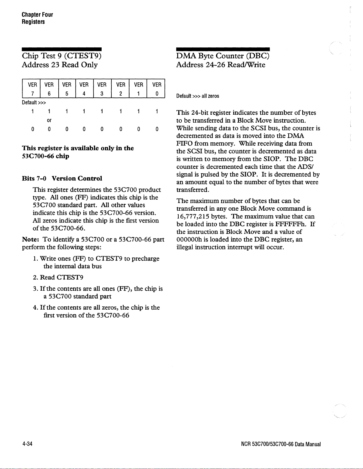
Chapter
Registers
Four
Chip Test 9
(CTEST9)
Address 23 Read Only
VER
VER VER VER
7 6 5 4 3 2 1 0
Default
»>
or
o
o o o o o o o
This
register
S3C700-66
Bits
7-0
This register determines the 53C700 product
type. All ones
53C700 standard part. All other values
indicate this chip
All
zeros indicate this chip
ofthe
Note:
To
perform the following steps:
is
available
chip
Version
Control
(FF)
53C700-66.
identify a 53C700
VER
only
VER
in
the
VER
indicates this chip
is
the 53C700-66 version.
is
the first version
or
a 53C700-66 part
is
VER
the
DMA
Byte
Counter
(DBC)
Address 24-26 ReadJWrite
Default
»>
all
zeros
This 24-bit register indicates the number
to be transferred in a Block Move instruction.
SCSI
While sending data to the
decremented as data
FIFO
the
is
counter
signal
from memory. While receiving data from
SCSI bus, the counter
written
to
memory from the SlOP.
is
decremented each time that the
is
pulsed by the SlOP.
is
moved into the
an amount equal to the number
bus, the counter
is
decremented
It
is
decremented by
of
bytes that were
transferred.
The
maximum number
transferred in
anyone
16,777,215 bytes.
be loaded into the
the instruction
OOOOOOh
is
is loaded into the
Block Move and a value
of
bytes that can be
Block Move command
The
maximum value that can
DBC
register
DBC
is
FFFFFFh.
register, an
illegal instruction interrupt will occur.
of
DMA
The
bytes
as
DBC
ADSI
of
is
data
is
If
1.
Write ones
(FF)
to
CTEST9
the internal data bus
2.
Read
CTEST9
3.
If
the contents are all ones
a 53C700 standard part
If
the contents are all zeros, the chip
4.
of
first version
the 53C700-66
to
(FF),
precharge
the chip
is
the
is
/-"
4-34
NCR
53C700/53C700-66
Data
Manual
Page 71
Chapter
Registers
Four
I'"
DMA
Command
CDCMD)
Address 27 ReadIWrite
Default
>>>
all
zeros
This contains the 8-bit opcode
instruction that has been fetched.
the first 8-bit field
For
tion.
please refer to the instruction set
Chapter 5.
a complete description
of
a 64-bit
of a SCRIPTS
SCRIPTS
The
opcode
instruc-
of
the opcodes,
of
the
SlOP
in
is
DMA
Next
Address for
Data
CDNAD)
Address 28-2B ReadIWrite
Default
»>
all
zeros
This 32-bit register contains the second longword
of
a SCRIPTS Block Move instruction. Block
Move instructions use this register to point to the
For
address where data is to be moved.
or
reselect, jump, call
tains a copy from
longword. This register should
written while executing
return instruction, it con-
the
DSPS
SCSI
register
not
SCRIPTS.
a select,
of
the second
be read or
(
NCR
53C700/53C700-66
Data
Manual
4-35
Page 72
Chapter
Registers
Four
DMA
Address
Default
To
first
to this register.
once the start address
written to this register, the
are automatically fetched and executed until an
interrupt condition occurs.
incremented immediately after the current instruction
the next instruction while the current instruction
is
In
step interrupt after each instruction
After the first instruction
register does
address,
register)
interrupt occurs to fetch and execute the next
SCRIPTS
SCRIPTS
2C-2F
>>>
all
zeros
execute
SCSI
is
executing.
single step mode, there
SCSI
SCRIPTS
fetched.
not
but
the
must
instruction.
be set each time the single step
Pointer (DSP)
ReadIWrite
SCRIPTS, the address
instruction should be written
In
normal
of
The
register will therefore point to
need to be written with the next
Start
DMA
SCRIPTS
the SCSI
SCRIPTS
The
is a SCRIPTS
is
executed, the
SCRIPTS
DSP
is
bit (bit 2,
ofthe
operation,
is
instructions
register is
single
executed.
DSP
DCNTL
DMA
SCRIPTS
Pointer Save (DSPS)
Address 30-33 ReadIWrite
Default
»>
all
zeros
This 32-bit register contains the second longword
of
a Select, Reselect, Jump, Call, Return,
Interrupt
fetched. When executing pipelined instructions
(Pipeline mode,
register should
longword
not
SCRIPTS.
be
read
SCRIPTS
of
the pipelined command.
or
instruction that has been
DMODE
be
loaded with the second
written while executing
register, bit
or
1)
this
It
should
SCSI
In
pipeline mode
register becomes the
The
write to the
instruction fetch. When writing this register 8-bits
at a time
should
or
be
written last.
(DCNTL
upper
16 bits
register, bit 1), this
DCMD
byte starts a
at
a time, the upper byte
and
DBC
SCRIPTS
register.
4-36
NCR
53C700/53C700-66
Data
Manual
Page 73
DMA
Address
Default
BL1
7 6
>>>
Mode
34
BW16
BLO
(DMODE)
ReadIWrite
286
5
o o o o o
101M
4 3
FAM
2
o
PIPE
1 0
o o
MAN
Bit
4 286 (286
Mode)
When set to 1, the
mode.
It
will connect directly to the Intel
80286 microprocessor.
change function:
BE2/ becomes BHEI,
BEI/
becomes
BEO/
becomes
SlOP
AI,
and
AO.
Chapter
Registers
operates in 80286
The
following signals
Four
Bit 7 BL1
Bit
6 BLO
Burst
Lengths
Bl1
0
0
1
1
(Burst
(Burst
Transferred
BlO
0
Length
Length
across
Bit
1)
Bit
0)
the
80386
Burst
length
1 Transfer
1 2 Transfers
0
4 Transfers
1 8 Transfers
Interface
These two control bits determine the maximum
data burst length transferred across the
The
80386 interface.
actual number
transferred across the bus
or
bus width (16-bit
32-bit) times the burst
is
equal to the host
of
length.
Once the
bus, it
is
complete.
Bit 5 BW16
SlOP
will stay
(Host
bits)
has won control
on
the bus until the data burst
Bus
Width
of
Equal
the host
to
When set to 1, during Block Move instructions
SlOP
the
allows the
memory. This bit does
SCRIPTS
SCSI
controls how
transfers data 16-bits at a time. This
SlOP
to
operate with 16-bit
NOT
cause SCSI
to be loaded 16-bits at a time.
SCRIPTS
16 bit in the
SCSI
SCRIPTS
DCNTL
are loaded.
bytes
16
The
register
Block Move instructions transfer data 16-bits
at a time and
SCRIPTS
instructions are
fetched 16-bits at a time. Initialize this bit
or
before reading
the
SlOP
needs to operate in 80286 mode.
writing any other register
This bit must be set again any time a software
is
reset
Bit 3 10/M
issued
This bit determines
to/from a memory-mapped address
mapped address when the
bus master. Writing this bit to 1
MIO/
signal low, transferring data to an I10-
(DCNTL,
(110
Mapped
Mapped)
if
or
data
bit 0).
Memory
is
to be transferred
or
SlOP
becomes a
will drive the
mapped device. Writing this bit to 0 will drive
the
MIO/
signal high, transferring data to a
memory-mapped device. This bit does not
an
effect
on
have
instruction fetch operations,
it only applies to data being transferred tot
no
affect
from memory. This bit has
the
SlOP's
addresses are mapped, this
on
determined by external address decode logic.
Bit 2 FAM
Writing this bit to 1 disables the
(Fixed
Address
Mode)
DMA
address pointer from incrementing after each
data transfer.
is
located in the
DMA
DNAD
next address pointer
register. Use fixed
The
addressing to transfer data to/from one port
address, i.e. a serial port.
this bit
is
If
next address pointer increments after each
data transfer.
an
I10-
how
is
next
0, the
if
(
NCR
53C700/53C700-66
Data
Manual
4-37
Page 74
Chapter
Registers
Four
Bit 1 PIPE
Setting this bit to 1 disables the automatic
fetch and execution
memory.
registers have different functions.
register operates as the first 32-bit word
pipelined instruction.
operates as
pipelined instruction.
pipelined commands are
1. Write this pipeline mode bit to 1.
2. Load
**3. Load
4. Write the start
5. Poll the Pipeline register Empty bit in the
6. Load the
7. Load the
8.
* Pipeline
next generation
**
cycle, the high byte (or word) must
written last.
Bit 0 MAN
Writing this bit to 1 disables the
automatically fetching
SCRIPTS
For
DCNTL
to start fetching and executing instructions.
Writing this bit to
matically fetch and execute
after the
(PipeJine
In
this mode, the
the
the
32-bit word
the
bit word
register, bit 2).
ISTAT
32-bit word
bit word
Go
If
the
of
register until it
to step 4.
Mode
DSP
(Manual
after the
this case, the Start
register must be set to 1 for the
DSP
Mode
of
second 32-bit word
DSPS register with the second
ofthe
DSP
register with the first 32-
the instruction.
DMA
DSPS
ofthe
DSP
register with the first 32-
of
the next instruction.
will
of
is
not
Start
DSP
0 causes the
Register
*)
SCSI
SCRIPTSTM from
DSP
The
DSPS
The
execution
as
follows:
instruction.
bit
register with the second
next instruction.
not
be offered in
the 53C700 family.
written in a single 32-bit
Mode)
and
executing
register
DMA
SCSI
is
written.
and
The
register
(DCN'lL
is
1.
SlOP
is
bit in the
SlOP
SCRIPTS
DSPS
DSP
of
of
a
of
the
be
from
SCSI
written.
SlOP
to
auto-
DMA
Interrupt Enable
(DIEN)
Register 39 ReadIWrite
RES
RES RES
a
7 6 5 4 3 2
Default
>>>
o o o o o o
Bits
7-5
RES
Bit 4 ABRT
Writing this bit to 1 asserts the IRQ! signal
an
abort condition. Abort conditions can
occur in two ways: the
is
signal
is
register. Writing
assertion
occurs.
Bit 3 SSI
Writing this bit to 1 asserts the IRQ! signal
when the
occurs. Resetting this bit to
assertion
Step Interrupt condition occurs.
ing conditions cause a Single
1.
2.
Bit 2 SIR
Writing this bit to 1 asserts the IRQ! signal
when the
Received bit
The
status bit
asserted
issued by writing 1 to Bit 7
of
(Enable
of
If
the Single Step
register
SCRIPTS
executing each instruction.
If
the
SlOP
while executing pipelined instructions
(Pipeline mode,
(Enable
SCRIPTS
ABRT
SSI
SIR
(Reserved)
(Enable
IRQ! when
Aborted
DP3
or
a software abort command
0 to this bit disables the
an
SCRIPTS
Interrupt)
_ ABRTI input
of
the 1ST A T
abort condition
Single
Interrupt)
SCRIPTS
IRQ! when a
is
equal to 1, then there will
Instruction
SCRIPTS
is
is
set when
Single Step Interrupt
0 disables the
SCRIPTS
The
Step interrupt .
Mode
Single Step Interrupt after
encounters a branch condition
DMODE
SCRIPTS
bit in the
register, bit 1).
Interrupt
Received
Interrupt Instruction
set
to
1 in the
Interrupt Instruction Received
an
DSTAT
interrupt instruction
WTD
OPC
1 0
o
o
on
Step
Single
follow-
DCNTL
be
a
Interrupt)
register.
4-38
NCR
53C700/53C700-66
Data
Manual
Page 75
Chapter
Registers
Four
occurs during execution
Writing 0 to this bit disables the assertion
IRQ! when a
is
received.
Bit 1 WTD
Writing this bit to 1 asserts the IRQ! signal
whenever the Watchdog
decremented
If
the counter decrements to zero, it indicates
that the memory device did not assert the
READYII signal within the specified time-out
period from the
Resetting this bit to 0 disables the assertion
IRQ! when a Watchdog Time-out condition
occurs.
Bit
0
ope
Writing this bit to 1 asserts the IRQ! signal
anytime that
This bit can be set when the
either
mode
disables the assertion
Instruction condition occurs.
SCSI
or
SCRIPTS
(Enable
Interrupt)
to
zero.
SlOP
(Enable
Interrupt)
an
illegal instruction
SCRIPTS
pipeline mode. Writing 0 to this bit
of
SCSI
SCRIPTS.
Interrupt instruction
Watchdog
Timer
assertion
megal
mode or Single Step
of
IRQ! when an Illegal
Time-out
Counter has
of
Instruction
SlOP
ADS/.
is
decoded.
operates in
of
of
DMA
Address
Default
The
time-out mechanism during data transfers between the
determines the amount
wait for the assertion
pulsing the
to this register during initialization. Every time
the
stored in this register
Disable the time-out feature by writing a
this register.
The
input periods.
period
16 x 20 nsec = 320 nsec.
was desired, then
be loaded with a value
Watchdog
3A
»>
all
zeros
DMA
SlOP
unit time base for this register
Watchdog
SlOP
ADS/ signal. Write the time-out value
transfers data to/from memory, the value
Timer
ReadIWrite
Timer
and
memory. This register
of
time that the
of
the READYII signal after
is
loaded into the counter.
For
example, at 50
(DWT)
Register provides a
SlOP
is
16
MHz
= 20 nsec), the time base for this register
If
at
50
MHz
of
9D
a time-out
this register should
hex.
of
OOh
CLK
(clock
50
J.lSec
will
to
is
(
NCR
53C700/53C700-66
Data
Manual
4-39
Page 76
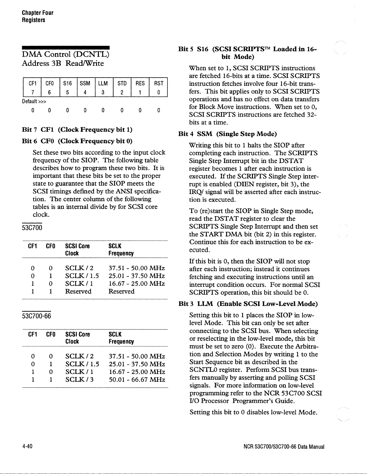
Chapter
Registers
DMA
Four
Control
(DCNTL)
Address 3B ReadIWrite
S16
CF1
CFO
7 6
Default
>>>
o 0 o o
Bit 7 CFl
Bit
6 CFO
(Clock
(Clock
SSM
5
Frequency
Frequency
4
LLM
3
o
bit
bit
Set these two bits according to the input clock
frequency
SlOP.
The
following table
of
the
describes how to program these two bits.
important that these bits
state to guarantee that the
SCSI
timings defined by the ANSI specifica-
The
tion.
tables
center column
is
an
internal divide by for
be
set to the proper
SlOP
of
the following
clock.
53C700
CF1
CFO
0 0
0
1
1
0
SCSI
Core
Clock
SCLK/2
SCLK/1.5
SCLK/l
SClK
Frequency
37.51 - 50.00
25.01 - 37.50
16.67 - 25.00
1 1 Reserved Reserved
RES
STD
2 1
o o o
1)
0)
meets the
SCSI
RST
It
core
MHz
MHz
MHz
Bit
5 S16
When set to 1,
are fetched 16-bits at a time.
(SCSI
bit
SCRIPTSTM
Mode)
SCSI
SCRIPTS
Loaded
instructions
SCSI
SCRIPTS
in
16-
instruction fetches involve four 16-bit trans-
SCSI
0
fers. This bit applies only to
operations
and
has no effect
on
for Block Move instructions. When set to
SCSI
SCRIPTS
instructions are fetched 32-
SCRIPTS
data transfers
0,
bits at a time.
is
Bit 4 SSM
Writing this bit to 1 halts the
completing each instruction.
Single Step Interrupt bit in the
register becomes 1 after each instruction
executed.
rupt
IRQ!
tion
To
read the
SCRIPTS
the
(Single
Step
Mode)
SlOP
The
after
SCRIPTS
DSTAT
If
the
is
enabled
SCRIPTS
(DIEN
Single Step inter-
register, bit 3), the
signal will be asserted after each instruc-
is
executed.
(re)start the
DST
START
SlOP
in Single Step mode,
A T register to clear the
Single Step Interrupt
DMA
bit (bit
2)
in this register.
and
then
is
set
Continue this for each instruction to be executed.
If
this bit
is
0,
then
the
SlOP
will
not
stop
after each instruction; instead it continues
and
fetching
executing instructions until
interrupt condition occurs.
SCRIPTS
operation, this bit should
For
normal SCSI
be
an
O.
53C700-66
CF1
CFO
0 0
0 1
1
0
1 1
4-40
SCSI
Core
Clock
SCLK/2
SCLK/1.5
SCLK/l
SCLK/3
SClK
Frequency
37.51 - 50.00
25.01 - 37.50
16.67 - 25.00
50.01 - 66.67
MHz
MHz
MHz
MHz
Bit 3 LLM
Setting this bit to 1 places the
level Mode. This bit can only
connecting
(Enable
to
the
SCSI
Low-Level
SlOP
be
SCSI
bus. When selecting
set after
or res electing in the low-level mode, this bit
must be set to zero
(0). Execute the Arbitration and Selection Modes by writing 1
Start Sequence bit as described in the
SCNTLO register. Perform
fers manually by asserting
signals.
For
more information
programming refer to the
110 Processor Programmer's Guide.
SCSI
and
NCR
bus trans-
polling
on
low-level
53C700
Setting this bit to 0 disables low-level Mode.
NCR
53C700/53C700-66
Mode)
in low-
to
the
SCSI
SCSI
Data
Manual
Page 77
Chapter
Registers
Four
Bit 2 STD
The
(Start
SlOP
fetches a SCSI
DMA
Operation)
SCRIPTS
tion from the address contained in the
register when this bit
required
if
the
SlOP
is
set to
is
in one
modes:
1. Manual Start Mode - Bit
0 in the
register equals 1
2. Single Step
Mode
- Bit 4
in
register equals 1
3. Pipeline
Mode
- Bit 1 in the
register equals 1
The
Start
start execution
SlOP
is
Mode,
bit
is
set to 1, it should not
again until
Bit 1 RES
Bit 0 RST
DMA
in Manual Start Mode, Single Step
or
Pipeline Mode after the Start
(Reserved)
(Software
bit needs to be written
of
each instruction.
an
interrupt occurs.
Reset)
be
instruc-
DNAD
1.
This bit
of
the following
DMODE
the
DCNTL
DMODE
to
If
the
DMA
written to 1
is
1 to
Scratch B (SCRATCHB)
Address
Default
This
53C700-66
This
pad
not destroy the contents
ReadlWrites into the
alter its contents. This register can
cessed by the internal
3C-3F
»>
all
zeros
register
ReadJWrite
is
available
only
in
chip
is
a general purpose user definable scratch
register. Normal
SCRIPTS
of
operations will
this register, only slave
SCRATCH
SCSI
I/O processor.
the
B register will
not
be ac-
Writing this bit
to
1 resets the
SlOP.
All
registers are cleared to their default values
(except the 286 bit in
DMODE)
and all
SCSI
signals are deasserted. Writing this bit to 1
not
does
become asserted. This bit
and
cause the SCSI RSTI signal to
is
must
be
written to 0 in order to clear the
not self-clearing
reset condition.
NCR
53C700/53C700-66
Data
Manual
4-41
Page 78

i
c
T
!
Page 79
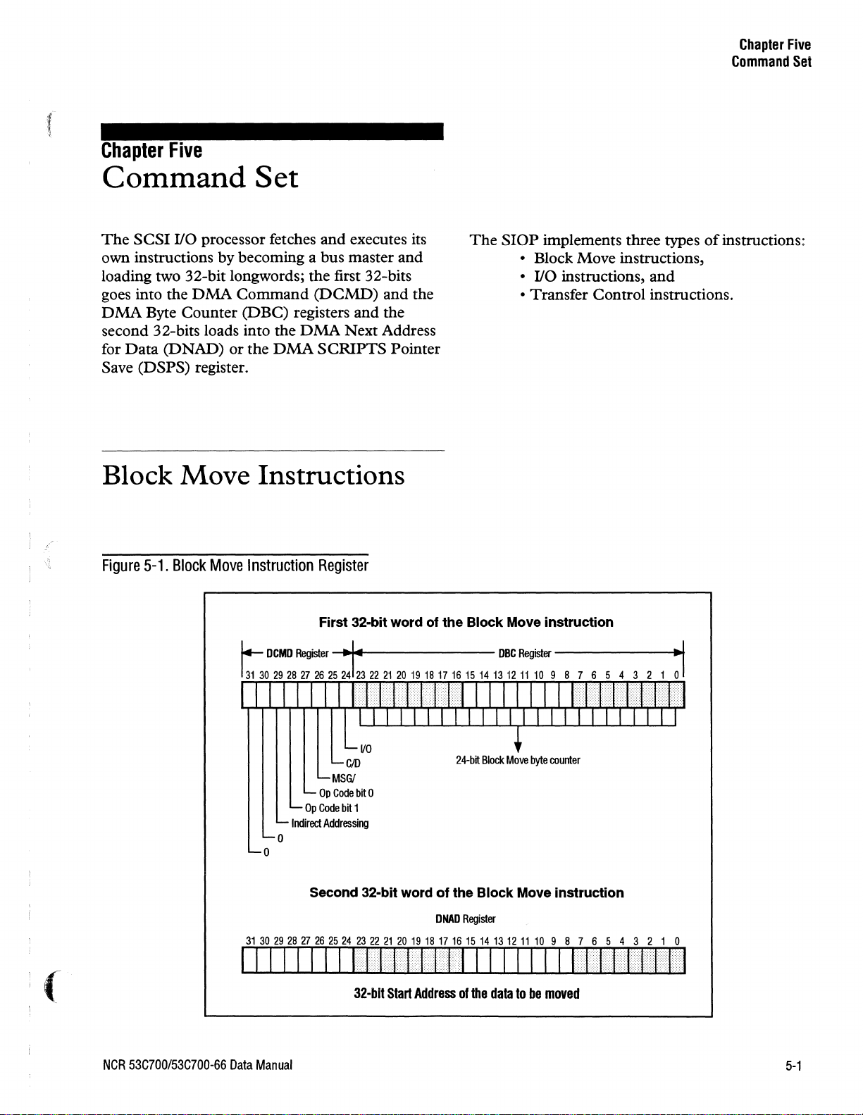
f
Chapter
Five
Chapter
Command
Five
Set
Command
The
SCSI
I/O processor fetches
Set
and
executes its
own instructions by becoming a bus master and
loading two 32-bit longwords; the first 32-bits
goes into the
DMA
Byte Counter (DBC) registers and the
DMA
second 32-bits loads into the
Data
for
Save
(DNAD)
CDSPS)
Command
or
register.
the
DMA
DMA
(DCMO)
Next Address
SCRIPTS
and the
Pointer
Block Move Instructions
Figure
5-1.
Block
Move
Instruction
Register
The
SlOP
implements three types
• Block Move instructions,
• I/O instructions,
and
• Transfer Control instructions.
of
instructions:
(
First 32·bit word
VO
C/O
MSGI
Op
Code
bit
Op
Code
bit
1
Indirect
Addressing
0
of
the Block Move instruction
24-bit
Block
Move
byte
counter
o
o
31
30
Second 32·bit word
29 28
'lJ
26 25
24 23 22
21
20
of
the Block Move instruction
DNAD
Register
19
18
17 16
15 14
131211
10
9 8 7 6 5 4 3 2 1 0
I I I I I I I I 1IIIIIIIql I I I I I I I
32·blt
Start
Address
01
the
data
to
be
moved
I~IIIIII)I
NCR
53C700/53C700-66
Data
Manual
5-1
Page 80
Chapter
Command
Five
Set
Indirect Addressing
Field (Bit 29)
When this bit
moved to or from the 32-bit data start address for
the Block Move instruction.
into the chip's address register and incremented
data
is
transferred.
When set to
for the Block Move instruction
pointer to the actual data buffer address.
value
at
chip's
DNAD
(four-byte transfers across the host computer bus).
This option implies three
fers, rather
Once the data buffer address
ecuted
as
mode. This indirect feature allows a table
buffer addresses to be specified. Using the
SCSI
SCRIPTS
placed in the script
actual data transfer time, the offsets are added to
the base address
external processor.
structure
treating each address individually.
makes
it
PROM.
is
cleared (set
1,
the 32-bit user data start address
the 32-bit start address
to
0), user data
The
value
is
the address
is
loaded into the
register via a second longword
DMA
than
only two transfers.
if
the chip was operating in the direct
longword trans-
is
loaded, it
compiler, the table offset
at
compile time.
ofthe
of
addresses for an 110 rather
data address table
The
logical 110 driver builds a
Then
This
possible
to
locate
SCSI
SCRIPTS
is
loaded
The
is
ex-
of
NCR
is
at
by
than
feature
in a
is
of
data
the
the
as
a
Opcode Field (Bits 28, 27)
Target
Note:
Mode
OPC1
OPCO
o o
Instruction
Defined
MOVE - Block Move
Opcode 1, 2, and 3 are Reserved - Illegal
Instruction, Interrupt will occur.
MOVE
1.
Instruction
If
the Indirect Addressing bit
is
1, the
fetches the starting address from the location
pointed to by the
in
the
DNAD
2.
The
SlOP
verifies that any previous Perform
DNAD
register.
register
and
Reselection command has been completed or
that the
SlOP
has been selected
as
a target
before starting to execute this instruction.
The
3.
SlOP
(MSG/,
asserts the
CID, & 110)
SCSI
as
defined
phase signals
by
the Phase
Field bits in the instruction.
If
the instruction
4.
(MSGI
= 0, CID =
waits for the first command byte
and decodes its
A.
If
the
SCSI
Group
SlOP
length
overwrites the
of
10,
or
6,
is
for the
1,
& 110 = 1), the
SCSI Group Code.
Group Code
1,
Group 2, or
DBC
the
Command
12 bytes.
command
to
be received
is
either
Group
5,
then
register with the
Descriptor Block,
SlOP
stores it
phase
SlOP
Group
the
0,
This two-bit field defmes the instruction to
executed.
meaning depending on whether the
operating in the initiator
5-2
The
Opcode Field bits have a different
SlOP
or
the target mode.
is
be
If
any other Group Code
B.
DBC
SlOP
register
will request the
is
specified in the
C.
If
the
Group
Code
Codes defined above in
DBC
register contains
not modified
DBC
number
register.
is
not
"A."
OOOOOOh,
is
received, the
and
of
one
ofthe
and the
Illegal Instruction Interrupt is generated.
NCR
53C700/53C700-66
the
bytes
Group
then an
Data
Manual
Page 81
5.
The
SlOP
transfers
specified in
address specified in the
If
the
6.
Initiator
OPC1
SCSI
initiator
transfer,
and
an interrupt generated.
on
Parity
register controls whether
generated.
Mode
------~-------------------
o
o
the
DBC
ATNI
or
a parity error occurred during the
the
transfer can optionally be halted
Error
or A TN
OPCD
o
1
Instruction
Reserved,
MOVE
the
number
register starting
DNAD
signal
is
asserted by
The
bit in
an
interrupt will be
Defined
DO
- Wait Block Move
instruction
of
bytes
register.
Disable
the
SXFER
NOT
at
the
use
the
Halt
5.
If
the
SCSI
in the
the
register starting
the
If
6.
stored in
generates a
7.
If
8.
SSTAT2
number
DNAD
the
SCSI
the
command
the
SCSI
not
deassert the last
deassert
instruction should
the host processor
byte(s).
During
assertion
deassert A
transfer,
the
the Message-Out phase, following
of
but
phase bits
of
bytes specified in the
register.
phase bits
SSTAT2
Phase
is
not
phase
last ACKI, a
ATN,
TN
during
before
match
register,
at
the
address
do
register,
Mismatch
executed.
is
Message-In,
ACKI
be
executed.
to
evaluate
the
SlOP
the
ACKI
the
not
Chapter
Command
the
value stored
SlOP
will transfer
DBC
pointed
match
the
Interrupt
of
the
CLEAR
the
will automatically
last handshake
is
asserted.
to
the
SlOP
and
the
SlOP
transfer.
ACK
This
allows
Message-In
Five
by
value
the
will
To
the
of
the
Set
(
Note:
Instruction,
MOVE
1.
2.
3.
4.
Opcodes 2
and
Interrupt
3 are Reserved -
will occur.
Instruction
If
the Indirect Addressing bit
fetches
pointed
in
The
Selection
that
tor
The
phase
is
means
for the corresponding phase
with an
target.
The
DCMD
lines stored in
phase lines are latched
asserted.
the
starting address from the location
to
by
the
DNAD
the
DNAD
SlOP
the
before executing this instruction.
SlOP
to
defined
that
ACKI
SlOP
register.
verifies
command
SlOP
waits for a previously unserviced
occur. A previously unserviced phase
as
the
compares
register with
that
has
been
any phase with REQI asserted.
SlOP
to
a
REQI
the
SSTAT2
An
is
1, the
SlOP
register,
any previous Perform
has
been
reselected
has
not
received by
the
SCSI
the
latched
when
and
completed
as
an
transferred
by
responding
the
phase bits in
SCSI
register.
REQI becomes
These
Illegal
stores it
or
initia-
It
data
the
phase
Phase Field (Bits 26-24,
MSG,
This
information transfer phase.
operates in initiator
with the
register.
the
The
nations
Information
MSG
Key:
CID,
three-bit field defines
SlOP
following table describes
and
0
0
0
0
1
1 0
1 1
1 1 1
"0"
& 110)
mode,
Latched
When
asserts
Transfer
CID
0 0
0
1
1 1
0 0 Reserved for future
equals
SCSI
phase bits in
the
SlOP
the
phase defmed in this field.
their corresponding
Phases
1/0
1
0
1
0 Message-Out
not
asserted,
the
When
these bits are
operates in target
SCSI
Data-Out
Data-In
Command
Status
Reserved for future
Message-In
desired
the
Phase
"1"
SCSI
the
SlOP
the
SST A T2
possible combi-
SCSI
phase.
equals asserted
compared
mode,
use
use
NCR
53C700/53C700-66
Data
Manual
5-3
Page 82
Chapter
Command
Five
Set
Transfer
DBC
A twenty-four-bit field specifying the
data bytes to be moved between the
system memory.
register. When the
memory, the
number
address in the
the
number
repeated until the
decremented
fetches the next instruction. Once the
started executing
not
write to the
Counter
register)
The
DBC
register
of
bytes transferred.
DNAD
of
bytes transferred. This process
DBC
to
zero. At that time, the
SCSI
DBC
Field (Bits 23-0,
SlOP
field
is
stored in the
SlOP
transfers data to/from
is
decremented
In
addition, the
register
register has been
SCRIPTS
register.
is
incremented by
instructions, do
number
and
DBC
by
SlOP
SlOP
Start Address Field (Bits 31-0,
DNAD
This 32-bit field specifies the starting address
the data
is
stored in the
transfers data to/from memory, the
ter
ferred.
SCRIPTS
register.
register)
to
be moved to/from memory.
DNAD
is
incremented by the number
Once the
instructions, do
register. When the
SlOP
has started executing
not
The
DNAD
of
bytes trans-
write to the
SlOP
regis-
DNAD
of
the
is
has
of
field
SCSI
5-4
NCR
53C700/53C700-66
Data
Manual
Page 83
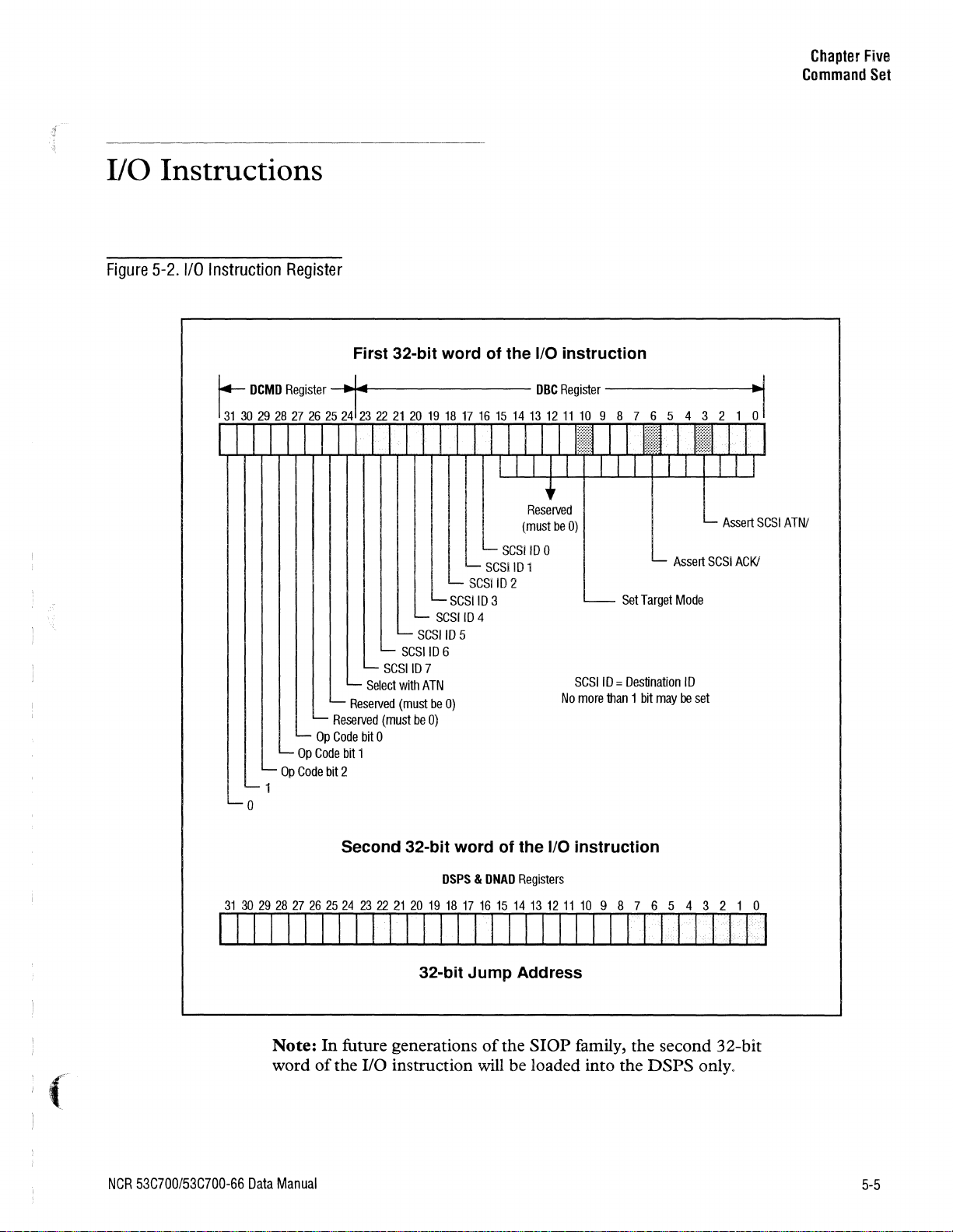
I/O Instructions
Figure
5-2.
I/O
Instruction
Register
Chapter
Five
Command
Set
o
Op
Op
Op
Code
Code
First 32-bit
Select
Reserved
Reserved
Code
bit
bit
1
bit
2
SCSIID
SCSIID7
with
(must
(must
0
word
SCSIID4
SGSIID
6
ATN
be
be
0)
SCSIID
SCSIID
5
0)
of
the I/O
SGSIID
SCSIID
2
3
Reserved
(must
be
0
1
instruction
0)
SetTarget
SCSIID = Destination
No
more
than 1 bit
may
Assert
Mode
ID
be
set
Assert
SCSI
SCSI
ACKJ
ATN!
(
NCR
53C700/53C700-66
31
30
29 28 27 26
Second 32-bit
2524 232221
DSPS & DNAD
20
19
18 17 16 15
word
of
the
Registers
14 13
I/O
12
1 I I I I I I I I III i I I II I I I
Data
Note:
word
Manual
32-bit
In
future generations
of
the 110 instruction will be loaded into the
Jump
of
the
Address
SlOP
instruction
11
10
9 8 7 6 5 4 3 2 1 0
II
I I 111·llll!1
family, the second 32-bit
DSPS
only.
5-5
Page 84
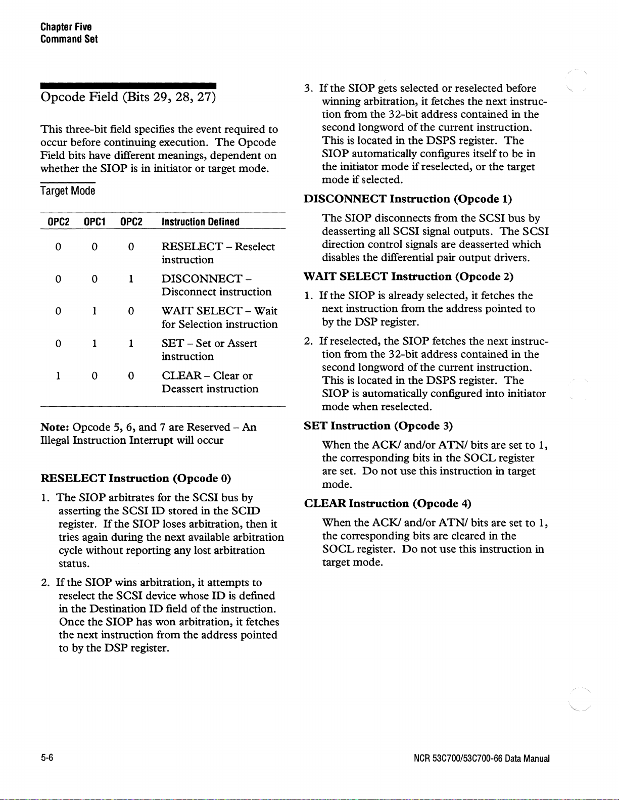
Chapter
Command
Five
Set
Opcode Field (Bits 29, 28, 27)
This three-bit field specifies the event required to
The
Defined
- Reselect
or
Assert
Opcode
on
-
- Wait
or
occur before continuing execution.
Field bits have different meanings, dependent
whether the
Target
OPC2
0 0 0
Mode
OPC1
SlOP
OPC2
is
in initiator or target mode.
Instruction
RESELECT
instruction
0 0
1
DISCONNECT
Disconnect instruction
0
1
0
WAIT
SELECT
for Selection instruction
0 1
1
SET
- Set
instruction
1
0
0
CLEAR
- Clear
Deassert instruction
3.
Ifthe
SlOP
gets selected
or
reselected before
winning arbitration, it fetches the next instruction from the 32-bit address contained in
second longword
This is located in the
SlOP
automatically configures itself to be in
the initiator
if
mode
selected.
DISCONNECT
The
SlOP
disconnects from the
deasserting all
of
the current instruction.
DSPS
mode
if
reselected,
Instruction
SCSI
signal outputs.
register.
or
the target
(Opcode
SCSI
1)
The
direction control signals are deasserted which
disables the differential pair
WAIT
1.
SELECT
If
the
SlOP
Instruction
is
already selected, it fetches the
next instruction from
2.
by the
If
DSP
register.
reselected, the
SlOP
the
output
drivers.
(Opcode
address pointed
fetches the next instruc-
tion from the 32-bit address contained in the
of
second longword
is
This
SlOP
located in the
is
automatically configured into initiator
the current instruction.
DSPS
register.
mode when reselected.
the
The
bus by
SCSI
2)
to
The
Note: Opcode 5,
6,and
7 are Reserved - An
megal Instruction Interrupt will occur
RESELECT
1.
The
SlOP
asserting the
register.
Instruction
(Opcode
arbitrates for the
SCSI
ID
stored in the
lfthe
SlOP
loses arbitration,
SCSI
0)
bus by
SCID
tries again during the next available arbitration
cycle without reporting any lost arbitration
status.
2.
lfthe
SlOP
wins arbitration, it attempts
reselect the
in the Destination
Once the
SCSI
device whose
ID
field
SlOP
has won arbitration, it fetches
ID
of
the instruction.
is
defined
the next instruction from the address pointed
DSP
to by the
register.
then
to
it
SET
Instruction
When the
the corresponding bits in the
are set.
Do
(Opcode
ACKI
and/or A
3)
TN/
bits are set
SOCL
not
use this instruction in target
mode.
CLEAR
Instruction
When the
ACKI
(Opcode
and/or
4)
ATN/
bits are set
the corresponding bits are cleared in the
SOCL
register.
Do
not
use
this instruction in
target mode.
to
register
to
1,
1,
./
5-6
NCR
53C700/53C700-66
Data
Manual
Page 85
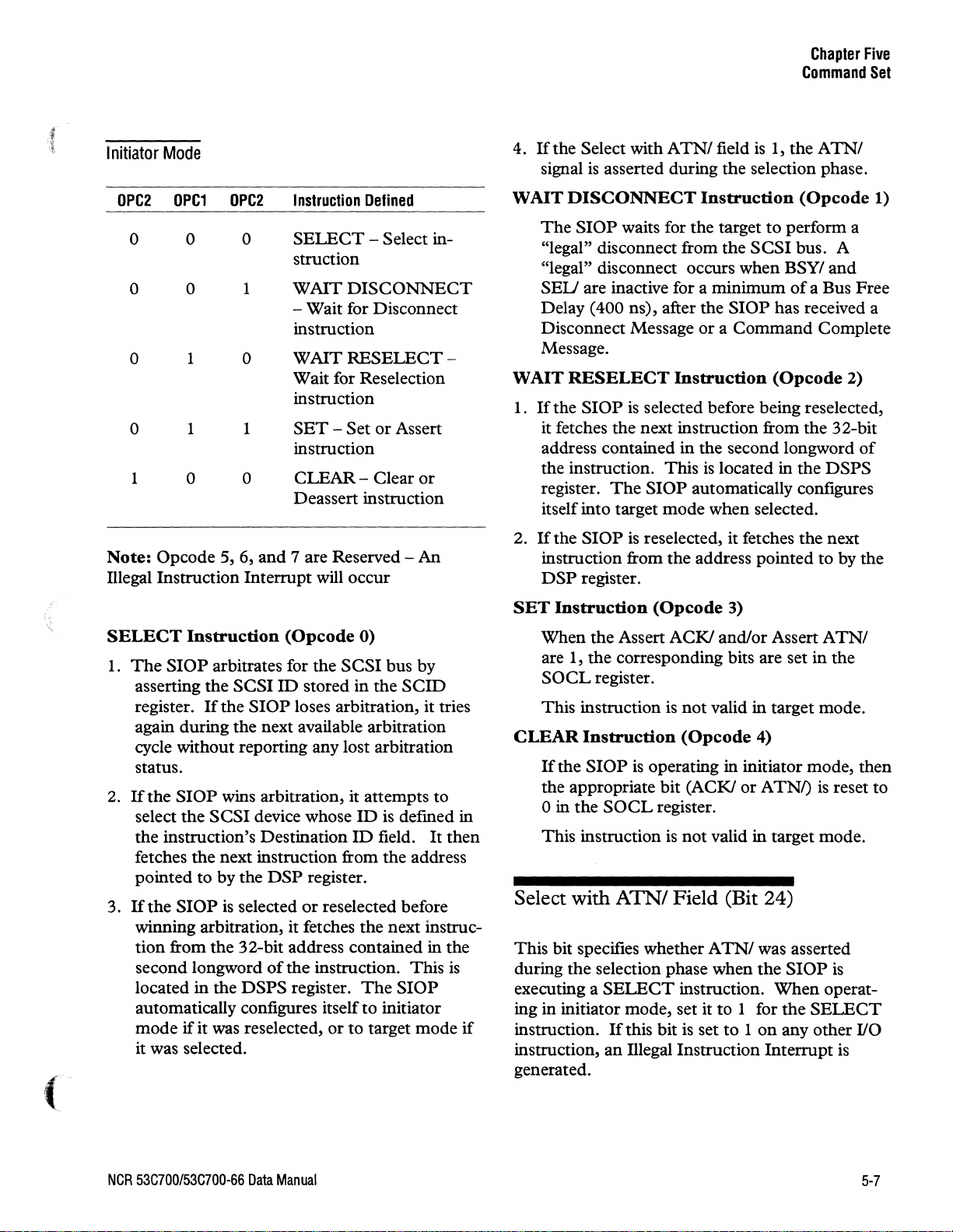
Chapter
Command
Five
Set
If
"
Initiator
Mode
OPC2
OPC1
0 0 0
OPC2
Instruction
SELECT
Defined
- Select in-
struction
0 0
1
WAIT
DISCONNECT
- Wait for Disconnect
instruction
0 1 0
WAIT
RESELECT
Wait for Reselection
instruction
SET
- Set
0 1 1
or
instruction
1 0 0
CLEAR - Clear
Deassert instruction
Note:
Opcode 5, 6, and 7 are Reserved -
Illegal Instruction Interrupt will occur
Assert
or
An
4.
If
the Select with A
signal
WAIT
The
is
asserted during the selection phase.
DISCONNECT
SlOP
waits for the target
"legal" disconnect from the
"legal" disconnect occurs when BSY/
SEU
are inactive for a minimum
Delay
(400 ns), after the
Disconnect Message
-
Message.
WAIT
1.
Ifthe
RESELECT
SlOP
is
TN/
field
is
1, the A
Instruedon
to
SCSI
TN/
(Opeode
perform a
bus. A
1)
and
of
a Bus Free
SlOP
has received a
or a Command
Instruedon
Complete
(Opeode
2)
selected before being res elected,
it fetches the next instruction from the 32-bit
address contained in the second longword
the instruction. This
register.
The
SlOP
is
located in the
automatically configures
of
DSPS
itself into target mode when selected.
2.
If
the
SlOP
is
res elected, it fetches the next
instruction from the address pointed to by the
DSP
register.
SELECT
1.
The
asserting the
register.
Instruedon
SlOP
arbitrates for the
SCSI
If
the
(Opeode
0)
SCSI
ID
stored in the
SlOP
loses arbitration, it tries
bus by
SCID
again during the next available arbitration
cycle without reporting any lost arbitration
status.
2.
If
the
SlOP
select the
the instruction's Destination
fetches
pointed to by the
3.
If
the
SlOP
wins arbitration, it attempts to
SCSI
device whose
the
next instruction from the address
DSP
register.
is
selected
or
ID
is defined in
ID
field.
reselected before
winning arbitration, it fetches the next instruction from the 32-bit address contained in the
of
second longword
located in the
the instruction. This
DSPS
register.
The
SlOP
automatically configures itself to initiator
if
mode
it was reselected,
or
to target mode
it was selected.
It
then
is
if
SET
Instruedon
When the Assert
(Opeode
ACKI
3)
and/or Assert A
are 1, the corresponding bits are set in the
SOCL
This instruction
CLEAR
If
the appropriate bit
o in the
This instruction
Select with
This bit specifies whether A
during the selection phase when the
executing a
register.
Instruedon
the
SlOP
SOCL
SELECT
is
not valid in target mode.
(Ope
ode
4)
is
operating in initiator mode, then
(ACKI
or A TN/)
register.
is
not valid in target mode.
ATNI
Field (Bit 24)
TN/
was asserted
SlOP
instruction. When operating in initiator mode, set it to 1 for the
instruction.
instruction,
If
this bit
an
Illegal Instruction Interrupt
is
set to 1
on
any other I/O
generated.
TN/
is
reset to
is
SELECT
is
NCR
53C700/53C700-66
Data
Manual
5-7
Page 86
Chapter
Command
Five
Set
SCSI
Destination
ID
Field (Bits 23-
16)
This eight-bit field specifies the destination SCSI
ID
for an I/O instruction. Set only one bit in this
field to 1.
SET
To
The
bit or bit
Assert
Target Role (Bit 9)
enable the
1. This sets bit 0
SlOP
SlOP
remains in target device mode until this
0 in the SCNTLO register
ACKI
as a target device set bit 10 to
of
the SCNTLO register to 1.
is
reset to
(Bit 6) & Assert
ATNI
o.
(Bit 3) Fields
Use these bits during the Set
10,
on
Bit
role. Bit
Bit 3,
places the chip in the target/initiator
6,
on sets/resets the SCSI acknowledge.
on
sets/resets the
SCSI
or
Clear command.
attention.
Jump
This thirty-two-bit field specifies the address
the instruction to fetch when the
a jump condition.
from the address pointed
the
different from the condition specified in the
instruction.
For
instruction in initiator mode,
reselected, then the next instruction
from the address pointed to by the jump address
field.
jump conditions, refer to the description
instruction.
Address Field
The
SlOP
fetches instructions
to
by this field whenever
SlOP
encounters a
example, during the execution
For
a complete description
SCSI
condition
if
the
SlOP
encounters
that
is
of a SELECT
SlOP
is
is
fetched
of
the different
of
each
of
of
Writing any
resets the corresponding bits in the
Use the
TN!
A
edge to handshake bytes across the
Use the CLEAR instruction to deassert
and/or A
message-in byte has been verified for each separate
message data Block Move command.
tor has the opportunity to set attention before
acknowledging the last message byte
Move command.
detected on the message in operation, the AS-
SERT
acknowledge
Issue clear attention after the target has serviced
the request for a message out by the initiator.
ACKI and A
unless the
SCSI Loopback Enable bit
register.
SET
on the SCSI bus. Also, use set Acknowl-
SCSI A
these bits to 1 sets the SlOP,
SOCL
instruction to assert ACKI and/or
SCSI bus.
TN!
on
the
SCSI
bus after the last target
On
TN
is
TN!
SlOP
each byte,
is
issued before the clear
issued
to
accept the message.
are
not
asserted on the SCSI bus
is
operating as
an
is
1 in the
if
a parity error
initiator or the
of
or
register.
ACKI
The
initia-
a Block
CTEST4
is
5-8
NCR
53C700/53C700-66
Data
Manual
Page 87
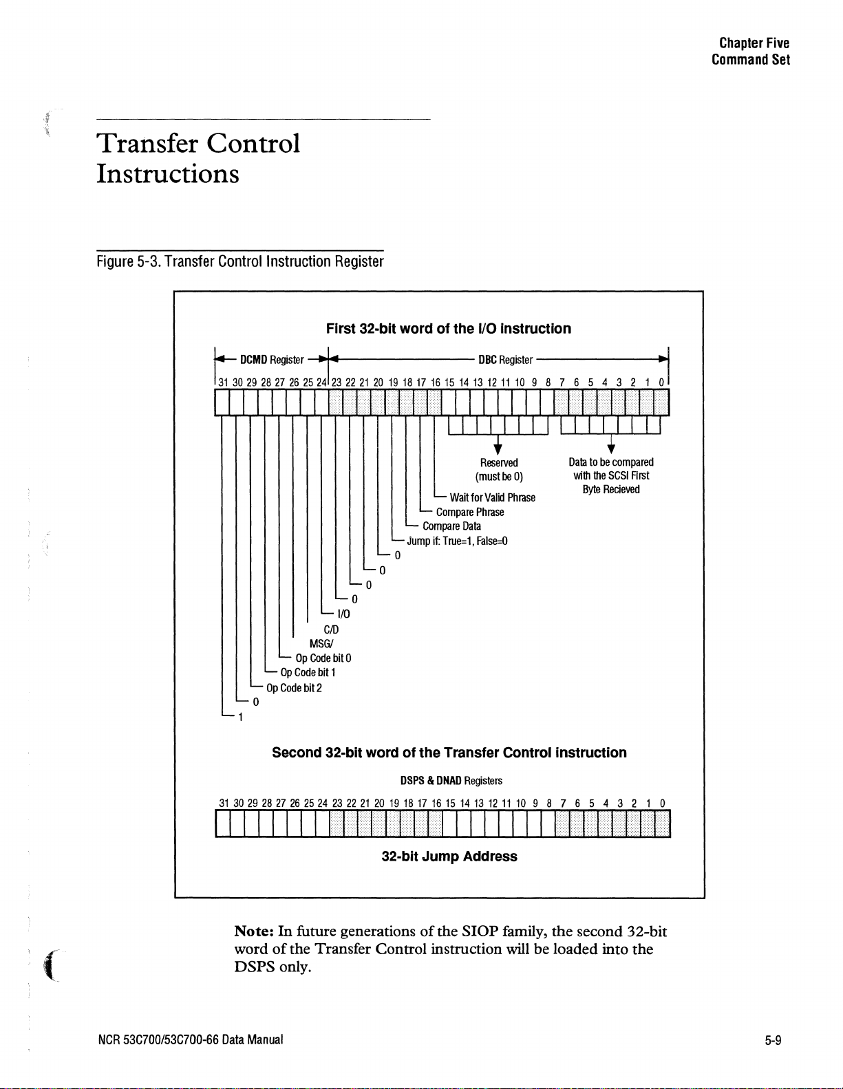
Chapter
Five
Command
Set
Transfer
Control
Instructions
Figure
5-3.
Transfer
Control
Instruction
Op
OpCodebit
Op
Code
o
Register
First 32·bit word
---'14--------
o
o
o
I/O
CID
MSG/
Code
bit
0
1
bit
2
o
Compare
Jump
of
the
WaitforValid
Compare
Data
if:
True=1.
1/0
Instruction
DOC
Register
Reserved
(must
be
0)
Phrase
Phrase
False=O
--------I~
Data
to
be
compared
With
the
SCSI
Byte
Recieved
Rrst
NCR
53C700/53C700-66
Note:
word
DSPS
Data
Second 32·bit word
In
future generations
of
the Transfer Control instruction will be loaded into the
only.
Manual
of
the Transfer Control instruction
DSPS & DNAD
Registers
32·bit Jump Address
of
the
SlOP
family,
the
second 32-bit
5-9
Page 88
Chapter
Command
Five
Set
Opcode Field (Bits 29, 28, 27)
This field specifies the type
instruction to be executed.
instructions can be conditional. They can be
dependent on a comparison
tion transfer phase with the Phase Field and/or a
of
comparison
the First Byte Received with the
Data Compare field. Each instruction operates in
the initiator or the target mode.
Transfer
Opcode
OPC2
Note:
Dlegal
JUMP
1.
Control
Field
OPC1
0 0 0
0
0 1 0
0
Instructions
Definitions
OPC2
0
1 1
1
Opcode hex 4-7 are Reserved Instruction Interrupt
Instruction
The
SlOP
compares the phase and/or data
(Opcode
defined by the Phase Compare, Data Compare
and TruelFalse bit fields.
are true, the
the contents
SlOP
of
the second longword
current instruction which
address.
address
2.
If
the comparisons are false, the
The
DSP
of
the next instruction.
the next instruction from the address pointed
to by the
DSP
register leaving the instruction
pointer unchanged.
of
transfer control
All
transfer control
of
the SCSI informa-
-
Instruction
JUMP
Defined
- Jump instruc-
tion
CAlL
RETURN
- Call instruction
- Return
instruction
INT
- Interrupt instruc-
tion
If
used, an
will
occur.
0)
If
the comparisons
loads the
DSP
register with
of
is
the 32-bit jump
the
register now contains the
SlOP
fetches
as
CALL
1.
Instruction
The
SlOP
(Opcode
1)
compares the phase and/or data
defmed by the Phase Compare, Data Compare, and TruelFalse bit fields.
parisons are true, the
DSP
value in
contents
TEMP
of
the second longword
instruction which
The
DSP
register now contains the address
SlOP
and then loads the
is
the 32-bit call address.
If
the com-
saves the current
of
the current
the next instruction.
A. When the
SlOP
executes a
CAlL
tion, the instruction pointer contained in
DSP
the
register
is
stored in the
TEMP
register.
B. When a
RETURN
the value stored in the
returned to the
2.
If
the comparisons are false, the
instruction
DSP
register.
TEMP
SlOP
is
executed,
register
the next instruction from the address pointed
DSP
to by the
RETURN
1.
The
SlOP
Instruction
register.
(Opcode
2)
compares the phase and/or data
defined by the Phase Compare, Data Compare, and TruelFalse bit fields.
parisons are true, then the
DSP
register with the contents
address stored in the
TEMP
address value becomes the address
SlOP
of
register.
If
the com-
loads the
the return
of
instruction.
A.
When the
SlOP
executes a
CAlL
tion, the current instruction pointer contained in the
TEMP
B. When a
the value stored
returned to the
C.
The
SlOP
the
CAlL
executed.
if
a
RETURN
without previously executing a
DSP
register
is
stored in the
register.
RETURN
instruction
in
the
DSP
register.
TEMP
is
executed,
register
does not check to see whether
instruction has already been
It
will
not
generate an interrupt
instruction
is
executed
CAlL
instruction.
as
DSP
of
instruc-
is
fetches
as
That
the next
instruc-
is
5-10
NCR
53C700/53C700-66
Data
Manual
Page 89
Chapter
Command
Five
Set
It
2.
If
the comparisons are false, then the
fetches the next instruction from the address
DSP
The
register
register.
3)
SlOP
IRQ!
of
the
INT
NOP
code, the second
DSPS
interrupt
must
Data
If
the com-
generates
signal.
instruction
is
loaded into
register.
must
be written to
pointed to by the
INT
Instruction
1.
The
SlOP
defmed by the
and
pare,
parisons are true, then the
interrupt by asserting the
2.
The
second longword
a 32-bit field that can contain a unique interrupt service vector. This value
DSPS
the
rupt, this unique status code allows the
quickly identify the point at which the interrupt occurred.
After any interrupt or
longword will be in the
3.
The
SlOP
and
viced
start any further operation.
(Opcode
compares the phase and/or data as
Phase Compare,
TruelFalse bit fields.
register. When servicing the inter-
halts.
the
DSP
SlOP
Com-
ISR
be ser-
an
to
is
Information
MSG
0 0 0
0 0
0
0
1
1
1 1
1 1
Key:
CIO
"0"
Transfer
110
1 0
1
0
0
equals
not
Phases
SCSI
Data-Out
1 Data-In
Command
1
0
1 Reserved for future use
0
1 Message-In
Status
Reserved for future use
Message-Out
asserted,
Jump if TruelFalse Field (Bit 19)
This field determines
when a comparison
is
false.
is
if
the
true
Phase
"1"
equals asserted
SlOP
or
should branch
when a comparison
Phase Field (Bits 26, 25, 24)
This three-bit field corresponds to the three SCSI
is
bus phase signals which
phase lines latched when REQ!
parisons can be performed to determine the SCSI
phase actually being driven
each phase signal, 1 = active
The
following table describes
and
nations
These bits are only valid when the
ing in initiator mode. When the
in the target mode, these bits are
should be written to
their corresponding
compared with the
is
on
the
and
the
SCSI
o.
asserted. Com-
SCSI
bus.
0 = inactive.
possible combi-
phase.
SlOP
is
operat-
SlOP
not
is
operating
valid
and
For
If
this bit
SlOP
cruMP,
SlOP
address contained in the second longword
current instruction. This
register.
new address.
If
this bit
SlOP
pointed to by the
If
this bit
SlOP
cruMP,
SlOP
pointed to by the
is 1 and
executes the Transfer Control instruction
CALL,
fetches the next instruction from the 32-bit
The
is 1 and
fetches the next instruction from the address
is 0 and
executes the Transfer Control instruction
CA.I..L,
fetches the next instruction from the address
the
comparison
RETURN,
is
located in the
instruction pointer will contain this
the comparison
DSP
register.
the comparison
RETURN,
DSP
register.
or
or
is
INT)
is
is
INT).
true, then
and
false, the
false, the
Then
the
of
the
DSPS
the
(
NCR
53C700/53C700-66
Data
Manual
5-11
Page 90
Chapter
Command
Five
Set
Compare
When this bit
from the
Data
(Bit 18)
is
1, then the first byte received
SCSI data bus is compared with the
Data
to be Compared Field in the Transfer Control
instruction.
Field.
this compare will occur.
Use this bit with the Compare Phase
The
Wait for a valid phase controls when
The
Jump ifTruelFalse
bit determines the condition (true or false) to
branch on.
This bit applies to both Phase Compares and
Compares.
If
both the Phase Compare and
Data
Data
Compare bits are set to 1, then both compares
on
must be true to branch
compares must be false
a true condition. Both
to
branch
on
a false
condition.
Compare Phase Field (Bit 17)
When the
controls compares
Information Transfer phase information. When
this bit
REQI
Transfer Control instruction.
latched by
then the comparison
If
the TruelFalse Field
Valid Phase controls when the compare will occur.
If
the Wait for Valid Phase bit
waits for a previously unserviced phase before
comparing the
If
the Wait for Valid Phase bit
compares the
SlOP
the
is
1, this field will test for
signal.
SlOP
is
in the initiator mode, this field
to
be performed on the SCSI
is
1, the
SCSI
phase signals latched by
are compared to the Phase Field in the
If
the phase signals
REQI
is
are identical to the Phase Field,
is
true.
is
1, then the Wait for a
is
1, then the
SCSI
phases.
is
0, then the
SCSI
phases immediately. When
operating in target mode and this bit
an
active
SCSI
ATNI
SlOP
SlOP
Compare
If
this bit
SCSI data bus
Data
is
1, then the first byte received from the
Field (Bit 16)
is
compared to the
Data
to be
Compared Field in the Transfer Control instruc-
The
tion.
Wait for a Valid Phase controls when
the compare will occur.
If
the Wait for Valid Phase bit
is
1, then the
SlOP
waits for a previously unserviced phase before
comparing the data.
If
the Wait for Valid Phase bit
is
0, then the
SlOP
compares the SCSI data immediately. This bit
can be used with the Compare Phase Field.
If
both the Compare
Data
Field and Compare
Phase Field bits are set, then the compare includes
both
the SCSI phase
If
the TruelFalse bit
and
the data byte.
is 1 and
the phase and data
are compared and determined to be identical, then
SlOP
the
fetches the next instruction from the
address pointed to by the 32-bit jump address
field.
If
the TruelFalse bit
the data are different, then the
is
1 and either the phase or
SlOP
fetches the
next instruction from the address pointed to by
DSP
the
If
the TruelFalse bit
register.
is
0, and either the phase or
the data do not match the compare fields, then the
SlOP
fetches the next instruction from the address
to
pointed
If
the TruelFalse bit
by the
the data are different, then the
DSP
register.
is
0, and both the phase and
SlOP
fetches the
next instruction from the address pointed to by
32-bit jump address field.
Mask for Compare
Data
(Bits 15-8)
5-12
The
mask bits allow selective comparison
within the data bytes using
compare, any bits that are
SCRIPTS. During the
on
cause the corre-
of
bits
sponding bit in the data byte to be ignored for the
comparison. A user can code a binary sort to
of
quickly determine the value
NCR
a byte.
53C700/53C700-66
Data
Manual
Page 91
Chapter
Command
Five
Set
[
For
instance, a mask
'80'
allows the
whether or not the high order bit
Data
This 8-bit field
first byte received register.
data pattern.
Jump
to
Compare
Address Field (Bits 31-0,
DNAD
This 32-bit field contains the address
instruction to fetch when the compare operations
are successful.
tion
is
issued, the Compare
bits are 1, and the
equal to the
SlOP
fetches the next instruction from this 32-bit
address.
SCRIPTS
be
Compared
Data
register)
Data
of
'7F'
and data compare
processor to determine
is
on.
Field (Bits 7-0)
is
the data compared to the SCSI
Use this bit with the
field to compare for a particular
of
the next
For
example,
SCSI
to be Compared field, then the
if
a
JUMP
Data
& TruelFalse
First Byte Received
instruc-
is
of
(
NCR
53C700/53C700-66
Data
Manual
5-13
Page 92

Page 93
Chapter
How
to
Six
Use
apter
How
This Chapter contains the following examples
how to use the
applies to both chips except where it says
66 only.
•
How
•
How
How to Execute Single-Step
•
• Steps Necessary to Start SCRIPTS
How
•
• How
How
•
•
How
• How to Abort an Operation
•
How
Six
to
Use
SlOP
to Start the
Mode
to Execute Normal SCRIPTS
to
Test the
to
Implement Parity Options
to
Test
to
Test
to Disconnect the
the
the
SlOP
SlOP
DMA
SCSI
the
chip. This information
in the SCSI
in the Loopback Mode
FIFO
FIFO
SlOP
53C700/53C700-66
53C700-
SCRIPTS
SCRIPTS
of
instruction
incremented by 8 and it points to the next SCSI
SCRIPTS address.
and execute instructions from system memory
until either an interrupt condition occurs or an
interrupt instruction
rupt
is
until the interrupt
halted, write the address
DSP
the
and execution
How
is
received, the
The
generated, the
is
register to restart the automatic fetch
of
the instructions.
DSP
register
SlOP
is
executed. Once an inter-
SlOP
serviced. Once the
of
continues to fetch
halts all operations
the next instruction in
is
to Execute Normal
SlOP
has
SCRIPTS
To
start
SCRIPTS
SCRIPTS address to the
for an interrupt
instructions, write the
DSP
register.
or
poll the
ISTAT
Then
register.
wait
•
How
to Select a Target
•
How
to
Reselect an Initiator
•
How
to
Respond to Multiple SCSI IDs
•
How
to
Use Single-Ended SCSI Interface
• How
•
How
SCSI
To
load the
containing the
The
address pointed to by the
to
Use Differential SCSI Interface
How
to Terminate the
to
Start
SCRIPTS
start the
DSP
SlOP
fetches the first instruction from the
the
SlOP
Mode
SlOP
in SCSI SCRIPTS mode, first
register with the address location
first SCSI
SlOP
Device
in
the
SCRIPTS
DSP
register. Once the
instruction.
How
to Execute Single-Step
SCRIPTS
To
execute single-step mode (one instruction at a
time) set bit 4 to 1 in the
start SCRIPTS instructions, write the
address to the
single-step interrupt. Execute subsequent instruc-
tions by setting the start
DCNTL
the
SCRIPTS instructions.
DSP
register. Repeat.until the
DCNTL
register.
DMA
Then
bit (bit
register.
SCRIPTS
wait for a
2)
to 1 in
end
To
of
the
NCR
53C700/53C700-66
Data
Manual
6-1
Page 94
Chapter
How
to
Six
Use
Steps Necessary to Start
SCRIPTS
5. Program
Bits
SIEN
(03h)
Description
/ -
'",
The
following list gives the programming steps for
initializing the
of
SCRIPTS instructions.
SlOP
1. Assert hardware
(DCNTL
Bits
register, bit
to start fetch and execution
or
software RESET
0)
Description
2 Fixed address mode
I/O
or
3
memory mapped
4 286 mode (16-bit device, set this
on
bit
the first register access after
a hardware reset)
5 Bus width 16
7 -6 Host burst length
2.
Program
DMODE
(34h)
6.
Program
0
1
Enable parity error interrupt
Enable SCSI RST! received inter
rupt
2 Enable unexpected disconnect
interrupt
3
4 Enable selected or reselected
Enable
SCSI gross error interrupt
interrupt
5
Enable selection or reselection
time-out interrupt
6
7 Enable phase mismatch or A
Enable function complete interrupt
active interrupt
SCID
Bits
(04h)
Description
TN!
3. Program
Bits
o Target mode
1
2
3
4. Program
Bits
5 Enable selection and reselection
SCNTLO
Description
Assert A
(OOh)
TN!
on
parity error
Enable parity generation
Enable parity checking
SCNTLI
Description
(Olh)
7-0
7. Program
Bits
3-0
6-4
7
Chip's
SXFER
Description
ID
(05h) *
Synchronous offset
Synchronous transfer period
on
Disable halt
a parity error or
ATN!
",-, /
6-2
NCR
53C700/53C700-66
Data
Manual
Page 95
Chapter
Howto
Six
Use
8. Program
Bits
o
1
2
8a. Program
53C700-66
Bits
4 Enable Active Negation
2 Shorten Request! Acknowledge
9. Program
CTEST7
Description
Enable differential
Enable
fetch
Enable even parity when sending
data
CTEST8
Description
filter
DIEN
(lBh)
DC/low
to
host bus
chip
(39h)
mode
for instruction
(22h)
only
11. Program
Bits
6-7 Clock frequency divide bits
12. Program
Bits
31-0 Start address
* Note: Synchronous offset
are normally set after synchronous negotiation
** Once
register that may
accessed once the scripts has been interrupted.
DCNTL
4
5
DSP
SCRIPTS
(3Bh)
Description
Single-step
Scripts loaded in 16-bit mode (only
for 386 mode)
(2Fh-2Ch) **
Description
is
be
read. Other registers may be
mode
of
script
and
transfer period
running 1ST
AT
is the only
(
Bits
o Enable illegal instruction interrupt
1 Enable watchdog timeout interrupt
2 Enable
3 Enable
4 Enable aborted interrupt
10. Program
Bits
7-0
Description
SCRIPTS
tion
received interrupt
SCRIPTS
interrupt
Dwr
(3Ah)
Description
Enter
watchdog timer period
interrupt instruc-
pipeline/step
How to Test the
SlOP
in the
Loopback Mode
SlOP
loopback mode allows testing
initiator
Loopback Enable bit
the
whether the
mode. Perform the following steps to implement
loopback mode.
1.
2. Set-up the desired arbitration mode
3. Set the Start Sequence bit in
and
target operations.
is
1 in the
SlOP
allows control
SlOP
Set the Loopback Enable
register
in the SCNTLO register.
register
to 1 .
to
1.
of
all
is
operating in initiator
bit
of
When
CTEST4
SCSI
signals,
in the
the
SCNTLO
both
the
register,
or
target
CTEST4
as
defmed
NCR
53C700/53C700-66
Data
Manual
6-3
Page 96
Chapter
How
to
Use
Six
4. Poll the
SEU
5. Poll the
SCSI
6.
In
in the
7. Poll the
determine when
To
8.
CID, and I/O bits to the desired phase in the
SOCL
9.
To
and set the REQI bit in the
1.
SBCL
is
active
SBDL
ID
register to determine when
and
BSYI
is
inactive.
register to determine which
bits are being driven.
response to selection, set the BSYI bit (bit
SOCL
assert the desired phase, set the
SEU
register to 1.
bit in the
SEU
SBCL
becomes inactive.
register to
MSG/,
register.
assert REQI, keep the phase bits the same
SOCL
To
accommodate the 400 ns bus settle
register to
delay, set REQI after setting the phase signals,
10.
The
initiator role can be implemented by
SCSI
single stepping
SlOP
How
can loopback as a target or vice versa.
to Implement Parity
SCRIPTS
and the
Options
3. Enable Parity Checking (EPC) - Bit 3 in the
SCNTLO register.
if
the
if
the
SlOP
checks for
SlOP
5)
4. Assert Even
This bit determines
The
parity errors.
SlOP
even parity depending on the status
Assert Even
SCSI Parity bit.
SCSI Parity (PAR) - Bit 2 in the
SCNTL1
register.
This bit determines
then asserts even or odd parity
register, bit 2).
5. Disable Halt on
Mode
Only (DHP) - Bit 7 in the
ATNI
or a Parity Error Target
register.
if
the
This bit determines
operations when a parity error
SlOP
is
target mode.
6. Enable Parity Error Interrupt (PAR) - Bit
the
SIEN
This bit determines
register.
if
the
SlOP
an interrupt when it detects a parity error.
7. Parity Error (PAR) - Bit
0 in the SSTATO
register.
will check for
odd
or
of
the
checks for and
SCNTL1
SXFER
will halt
detected in
0 in
will generate
The
SlOP
that allows control
parity
deliberately sent to the
error recovery procedures.
implements a flexible parity scheme
of
the type
is
checked, and whether a bad parity byte
SCSI
of
parity, whether
bus to test parity
The
parity options are
controlled by the following bits:
1.
Assert A
the
This control bit allows the
cally assert
parity error while the
TNI
on
Parity Errors (AAP) - Bit 1 in
SCNTLO register.
SCSI A
TNI
SlOP
to
when it detects a
SlOP
is
operating as an
automati-
initiator.
2.
Enable Parity Generation (EPG) - Bit 2 in the
SCNTLO register.
This bit controls whether the
to
parity sent
the SCSI bus
"flow through" the chip
SlOP
or
allows parity to
to/from
generates
the SCSI bus
and system bus.
is
This status bit
1 whenever the
SlOP
is
detected a parity error from either the
bus or the system bus.
Status
8.
the
This status bit represents the live
signal
9.
Latched SCSI Parity Signal (SDP) - Bit 3 in
the
of
SCSI Parity Signal (SDP!) - Bit 0 in
SSTAT1 register.
SCSI parity
(SDP/). When SDPI
is
active, it
SSTAT2 register.
This status bit represents the parity signal
(SDP!) after the First Byte Received
in the chip for a particular phase. When
is
10.
active, it
DMA
CTEST2
is
FIFO
register.
1.
Parity bit (DFP) - Bit 3 in the
This status bit represents the parity bit in the
DMA
by reading the
FIFO
after data
CTEST6
is
read from the
register.
has
SCSI
is
is
latched
SDPI
FIFO
1.
6·4
NCR
53C700/53C700·66
Data
Manual
Page 97
tf
.~
11.
DMA
CTEST7
FIFO
register.
Parity bit (DFP) - Bit 3 in the
Chapter
Howto
Six
Use
This write-only bit
FIFO
after writing data to the
writing the
SCSI
12.
CTEST2
FIFO
register.
CTEST6
is
written to the
DMA
DMA
register.
Parity bit (SFP) - Bit 4 in the
This status bit represents the parity bit in the
FIFO
SCSI
by reading the
after data
CTEST3
is
read from the
register.
FIFO
FIFO
by
NCR
53C700/53C700-66
Data
Manual
6-5
Page 98
Chapter
How
to
Six
Use
.'
/
How
Table
to Control Parity
6-1.
Parity
Control
EPG
(Parity
Generation)
0 0
0 0
0 1 0 0
0
EPC
(Parity
Checking)
1
Signals
AESP
(Even
Parity)
x
x 1
0
and
Descriptions
(Even
SCSI
EVP
Host
Parity)
0
Description
Parity pass through (DP3-DPO).
No
parity checking.
Odd
parity passed through the chip (DP3-DPO).
Parity pass through (DP3-DPO).
No
parity checking.
on
Host
SCSI
SCSI
Even parity asserted to
SCSI (done by inverting
Odd
parity asserted
(inverts Host bus parity).
Parity pass through (DP3-DPO).
Parity checking (always checks
Odd
parity throughout chip.
1 Parity pass through (DP3-DPO).
Parity checking (always checks
bus when receiving from
parity).
bus when sending to
odd
SCSI
parity).
odd
SCSI
parity).
SCSI
"
Odd
0 1
1
0
SCSI parity asserted on
sending data (inverts
Even parity asserted
SCSI
from
(inverts parity received from SCSI bus).
Host
on
Parity pass through (DP3-DPO).
SCSI
bus parity).
Host
bus when receiving data
Parity checking (always checks
Asserts even parity
on
SCSI
bus when sending data to
SCSI bus (inverts parity from host bus).
0 1 1 1 Parity pass through (DP3-DPO).
Parity checking (assuming
odd
Host bus, this configuration will always generate a
parity error when sending data to
on
SCSI
bus when sending data
Host
bus when receiving data
on
SCSI
1
0
0
x
Assert even parity
SCSI
to
Assert even parity
from
bus (inverts parity from
on
SCSI
bus (inverts parity from SCSI bus).
Parity generation (DP3-DPO ignored).
No
parity checking.
Odd
parity generated
bus when
odd
SCSI
parity).
parity received from
the
SCSI bus).
Host
bus).
bus.
6-6
NCR
53C700/53C700-66
Data
Manual
Page 99
Table
6-1.
Parity
Control
Signals
and
Descriptions
(Continued)
Chapter
How
to
Six
Use
EPG
(Parity
Generation)
1
1
1
Key:
EPG
EPC
AESP
EVP
EPC
(Parity
Checking)
o
1
1
AESP
(Even
SCSI
(Even
Parity) Parity)
1 x
o
1 x
EVP
x
= Enable Parity Generation
= Enable Parity Checking
= Assert
= Assert Even
SCSI
Host
Even Parity
Parity
Host
Description
Parity generation (DP3-DPO ignored).
No
parity checking.
Even parity generated
Parity generation
Parity checking.
Odd
Parity generation
Parity checking.
Even parity generated onto
Odd
(SCNTLO register,
(SCNTLO register,
(SCNTLI
(CTESTI
on
SCSI
bus.
(DP3-DPO ignored).
parity generated
parity checked when receiving data from
register,
register,
and
checked
(DP3-DPO ignored).
SCSI
bit
bit
bit
bit
2)
3)
2)
2)
1 = asserted
o = deasserted
x
=
on
bus.
don't
SCSI
care
bus.
SCSI
bus.
(
What Parity Errors and Interrupts Occur?
The
following table describes
when
a parity error occurs. This table only applies
to
the
case where
1 (SCNTLO register, bit 2).
Table
6-2.
Parity
DHP
o
o
1
1 1
Key:
DHP
EPI
the
Enable Parity Checking
Errors
and
EPI
o
1
o
Description
Will
Will interrupt when a parity error occurs in target
Will halt
interrupt
Will halt
target
= Disable
= Enable Parity
the
Interrupts
NOT
or
Halt
on A TN!
Interrupt
options available
bit
halt
when
a parity error occurs in target
when
a parity error occurs in target
when
a parity error occurs in target
initiator
mode
or
a Parity
is
Error
mode,
mode,
(SXFER
(SIEN
register,
or
initiator
or
initiator
will
NOT
will generate
register, bit 7)
bit
0)
mode
mode
generate
an
an
interrupt in
NCR
53C700/53C700-66
Data
Manual
6-7
Page 100
Chapter
How
to
Six
Use
How to Test the
The
DMA
FIFO.
The
FIFO
DMA
is
FIFO.
Figure
6-1.
DMA
FI
FO
I'"
T~--+-----f-----+------i
DMA
FIFO
more complex than the SCSI
FIFO
is
a 36-bit wide x 8 deep
Sections
It
can be divided into 4 sections, each being 9-bits
wide and 8 transfers deep.
of
Each
these four sections are labeled
as
Lanes." Each can be individually tested by writing known data into the
same data back out of the
36-bits
wide
------------II~~I
FIFO
FIFO.
and reading that
"Byte
8
transfers
1--------+--------4--------1--------1
deep
~~--+-----f-----+------i
~
To
write data into the
9-bits per instruction. Data
the
FIFO
FIFO. Three control bits in the
allow access to
Table
and
is
read from the bottom
anyone
6-3.
Byte
lane
FBl2
FBL1
0 X X Access disabled (set to this value before executing SCSI SCRIPTS)
9-bits
Byte
Lane
DMA
ofthe
Selection
FBlO
3
FIFO, load the data
is
written to the top
four "Byte Lanes."
Description
Byte
of
CTEST4
9-bits
Lane
the
register
9-bits
Byte
Lane
2
of
Parity
is
CTEST7
1
written to the
register. Set this bit to the desired value
before each write operation to the
To
the appropriate "Byte Lane", write the follow-
ing three bits
as
shown in Table 6-3.
Byte
FIFO
9-bits
Lane
--.f
0
through bit 3
FIFO.
of
the
X
6-8
1
1
1
0 0 Byte Lane 0
0 1
1
0
Byte Lane 1
Byte Lane 2
1 1 1 Byte Lane 3
=
Don't
Care
NCR
53C700/53C700-66
Data
--
,~
Manual
 Loading...