

Page 1
查询MM54C48供应商
MM54C48/MM74C48
BCD-to-7 Segment Decoder
MM54C48/MM74C48 BCD-to-7 Segment Decoder
March 1988
General Description
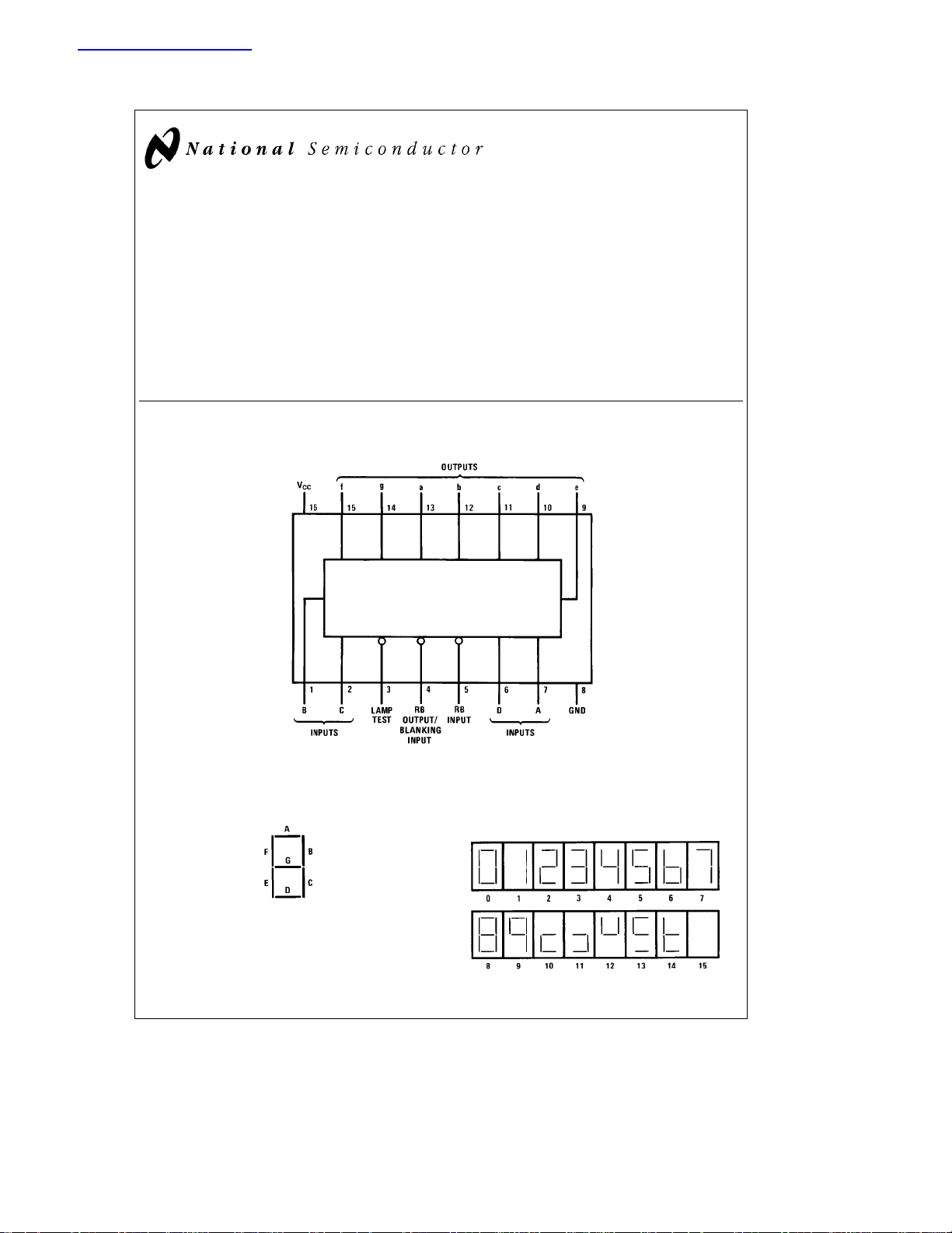
The MM54C48/MM74C48 BCD-to-7 segment decoder is a
monolithic complementary MOS (CMOS) integrated circuit
constructed with N- and P-channel enhancement transistors. Seven NAND gates and one driver are connected in
pairs to make binary-coded decimal (BCD) data and its complement available to the seven decoding AND-OR-INVERT
gates. The remaining NAND gate and three input buffers
provide test-blanking input/ripple-blanking output, and ripple-blanking inputs.
Connection Diagram
Dual-In-Line Package
Features
Y
Wide supply voltage range 3.0V to 15V
Y
Guaranteed noise margin 1.0V
Y
High noise immunity 0.45 VCC(typ.)
Y
Low power fan out of 2
TTL compatibility driving 74L
Y
High current sourcing output (up to 50 mA)
Y
Ripple blanking for leading or trailing zeros (optional)
Y
Lamp test provision
Top View
Order Number MM54C48 or MM74C48
Segment Identification
TL/F/5883– 2
C
1995 National Semiconductor Corporation RRD-B30M105/Printed in U. S. A.
TL/F/5883
Numerical Designations
and Resultant Displays
TL/F/5883– 1
TL/F/5883– 3
Page 2
Absolute Maximum Ratings (Note 1)
If Military/Aerospace specified devices are required,
please contact the National Semiconductor Sales
Office/Distributors for availability and specifications.
Voltage at Any Pin
Operating Temperature Range
MM54C48
MM74C48
Storage Temperature Range
b
0.3V to V
b
b
b
a
0.3V
CC
55§Ctoa125§C
40§Ctoa85§C
65§Ctoa150§C
Power Dissipation
Dual-In-Line 700 mW
Small Outline 500 mW
Operating V
Absolute Maximum V
Range 3.0V to 15V
CC
CC
Lead Temperature (Soldering, 10 seconds) 260
DC Electrical Characteristics Min/Max limits apply across temperature range unless otherwise noted
Symbol Parameter Conditions Min Typ Max Units
CMOS to CMOS
V
IN(1)
V
IN(0)
V
OUT(1)
V
OUT(0)
I
IN(1)
I
IN(0)
I
CC
Logical ‘‘1’’ Input Voltage V
Logical ‘‘0’’ Input Voltage V
Logical ‘‘1’’ Output Voltage V
(RB Output Only)
Logical ‘‘0’’ Output Voltage V
Logical ‘‘1’’ Input Current V
Logical ‘‘0’’ Input Current V
Supply Current V
CMOS/LPTTL INTERFACE
V
IN(1)
V
IN(0)
V
OUT(1)
V
OUT(0)
Logical ‘‘1’’ Input Voltage 54C, V
Logical ‘‘0’’ Input Voltage 54C, V
Logical ‘‘1’’ Output Voltage 54C, V
(RB Output Only)
Logical ‘‘0’’ Output Voltage 54C, V
OUTPUT DRIVE (See 54C/74C Family Characteristics Data Sheet)
I
SOURCE
I
SINK
I
SINK
I
SOURCE
Note 1: ‘‘Absolute Maximum Ratings’’ are those values beyond which the safety of the device cannot be guaranteed. Except for ‘‘Operating Temperature Range’’
they are not meant to imply that the devices should be operated at these limits. The table of ‘‘Electrical Characteristics’’ provides conditions for actual device
operation.
Note 2: Capacitance is guaranteed by periodic testing.
Note 3: C
AN-90.
Output Source Current V
(P-Channel)(RB Output Only)
Output Sink Current V
(N-Channel) T
Output Sink Current V
(N-Channel) T
Output Source Current V
(NPN Bipolar)
determines the no load AC power consumption of any CMOS device. For complete explanation see 54C/74C Family Characteristics Application Note,
PD
e
5.0V 3.5 V
CC
e
V
10V 8.0 V
CC
e
5.0V 1.5 V
CC
e
V
10V 2.0 V
CC
CC
V
CC
CC
V
CC
CC
CC
CC
74C, V
74C, V
74C, V
74C, V
CC
V
CC
CC
e
A
CC
e
A
CC
V
CC
V
CC
V
CC
e
e
e
e
e
e
e
e
e
e
25§C
e
25§C
e
e
e
e
eb
5.0V, I
10V, I
5.0V, I
10V, I
15.0V, V
15.0V, V
10 mA 4.5 V
O
eb
10 mA 9.0 V
O
e
10 mA 0.5 V
O
e
10 mA 1.0 V
O
e
15V 0.005 1.0 mA
IN
e
0V
IN
b
1.0
b
0.005 mA
15V 0.05 300 mA
e
4.5V V
CC
e
4.75V V
CC
e
4.5V 0.8 V
CC
e
4.75V 0.8 V
CC
e
CC
e
CC
e
CC
e
CC
4.75V, V
10V, V
5.0V, V
10V, V
5.0V, V
5.0V, V
10V, V
10V, V
4.5V, I
4.75V, I
4.5V, I
4.75V, I
OUT
OUT
OUT
OUT
OUT
OUT
OUT
OUT
eb
50 mA 2.4 V
O
eb
50 mA 2.4 V
O
e
360 mA 0.4 V
O
e
360 mA 0.4 V
O
e
0.4V
e
0.5V
e
V
CC
e
V
CC
e
3.4V
e
3.0V
e
8.4V
e
8.0V
b
1.5 V
CC
b
1.5 V
CC
1.75 3.6 mA
8.0 16 mA
b
20
b
20
b
50 mA
b
65 mA
b
50 mA
b
65 mA
b
0.80 mA
b
4.0 mA
18V
C
§
2
Page 3

AC Electrical Characteristics* T
e
A
25§C, C
e
50 pF, unless otherwise specified
L
Symbol Parameter Conditions Min Typ Max Units
t
pd0,tpd1
t
pd0
t
pd0
t
pd1
t
pd1
t
pd0
*AC Parameters are guaranteed by DC correlated testing.
Propagation Delay to a ‘‘1’’ or ‘‘0’’ on V
Segment Outputs from Data Inputs
Propagation Delay to a ‘‘0’’ on V
Segment Outputs from RB Input
Propagation Delay to a ‘‘0’’ on V
Segment Outputs from Blanking Input
Propagation Delay to a ‘‘1’’ on V
Segment Outputs from Lamp Test
Propagation Delay to a ‘‘1’’ on RB V
Output from RB Input
Propagation Delay to a ‘‘0’’ on RB V
Output from RB Input
e
5.0V 450 1500 ns
CC
e
10V 160 500 ns
V
CC
e
5.0V 500 1600 ns
CC
e
10V 180 550 ns
V
CC
e
5.0V 350 1200 ns
CC
e
10V 140 450 ns
V
CC
e
5.0V 450 1500 ns
CC
e
10V 160 500 ns
V
CC
e
5.0V 600 2000 ns
CC
e
10V 250 800 ns
V
CC
e
5.0V 140 450 ns
CC
e
10V 50 150 ns
V
CC
Typical Applications
Typical Connection Utilizing the Ripple-Blanking Feature
First three stages will blank leading zeros, the fourth stage will not blank zeros.
3
TL/F/5883– 4
Page 4

Typical Applications (Continued)
Blanking Input Connection Diagram
When RBO/BI is forced low, all segment outputs are off regardless of the state of any other input condition.
Light Emitting Diode (LED) Readout
TL/F/5883– 6
Incandescent Readout
Fluorescent Readout
TL/F/5883– 5
TL/F/5883– 7
**A filament pre-warm resistor is recommended to reduce filament thermal
shock and increase the effective cold resistance of the filament.
TL/F/5883– 8
TL/F/5883– 9
4
Page 5

Typical Applications (Continued)
Gas Discharge Readout
Liquid Crystal (LC) Readout
TL/F/5883– 11
TL/F/5883– 10
Direct DC drive of LC’s not recommended for life of LC readouts.
Truth Table
Decimal
or
Function
LT RBI D C B A a b c d e f g
0 H H L L L L H HHHHHHL 1
1 H X LL LH H LHHL LLL 1
2 H X LLHL H HHLHHLH
3 H X LLHH H HHHHLLH
4 H X LHLL H LHHLLHH
5 H X LHLH H HLHHLHH
6 H X L HHL H L LHHHHH
7 H X LHHH H HHHLLLL
8 H X HL L L H HHHHHHH
9 H X HLLH H HHHLLHH
10 H X HLHL H LL LHHLH
11 H X HLHH H LLHHLLH
12 H X HH L L H L HL L LHH
13 H X HH LH H H L LH LHH
14 H X HHH L H L L L HHHH
15 H X HHHH H LLLLLLL
BI X X XXXX L LLLLLLL 2
RBI H L LLLL L LLLLLLL 3
LT L X X XX X H HHHHHHH 4
Hehigh level, Lelow level, Xeirrelevant
Note 1: The blanking input (BI) must be open when output functions 0 –15 are desired. The ripple-blanking input (RBI) must be high, if blanking of a decimal
zero is not desired.
Note 2: When a low logic level is applied directly to the blanking input (BI), all segment outputs are low regardless of the level of any other input.
Note 3: When ripple-blanking input (RBI) and inputs A, B, C, and D are at a low level with the lamp-test input high, all segment outputs go low and the ripple-
blanking output (RBO) goes to a low level (response condition).
Note 4: When the blanking input/ripple-blanking output (BI/RBO) is open and a low is applied to the lamp-test input, all segment outputs are high.
²
One BI/RBO is wire-AND logic serving as blanking input (BI) and/or ripple-blanking output (RBO).
Inputs Outputs
BI/RBO
²
Note
5
Page 6

Physical Dimensions inches (millimeters)
Ceramic Dual-In-Line Package (J)
Order Number MM54C48J or MM74C48J
MM54C48/MM74C48 BCD-to-7 Segment Decoder
NS Package Number J16A
Molded Dual-In-Line Package (N)
Order Number MM54C48N or MM74C48N
NS Package Number N16E
LIFE SUPPORT POLICY
NATIONAL’S PRODUCTS ARE NOT AUTHORIZED FOR USE AS CRITICAL COMPONENTS IN LIFE SUPPORT
DEVICES OR SYSTEMS WITHOUT THE EXPRESS WRITTEN APPROVAL OF THE PRESIDENT OF NATIONAL
SEMICONDUCTOR CORPORATION. As used herein:
1. Life support devices or systems are devices or 2. A critical component is any component of a life
systems which, (a) are intended for surgical implant support device or system whose failure to perform can
into the body, or (b) support or sustain life, and whose be reasonably expected to cause the failure of the life
failure to perform, when properly used in accordance support device or system, or to affect its safety or
with instructions for use provided in the labeling, can effectiveness.
be reasonably expected to result in a significant injury
to the user.
National Semiconductor National Semiconductor National Semiconductor National Semiconductor
Corporation Europe Hong Kong Ltd. Japan Ltd.
1111 West Bardin Road Fax: (
Arlington, TX 76017 Email: cnjwge@tevm2.nsc.com Ocean Centre, 5 Canton Rd. Fax: 81-043-299-2408
Tel: 1(800) 272-9959 Deutsch Tel: (
Fax: 1(800) 737-7018 English Tel: (
National does not assume any responsibility for use of any circuitry described, no circuit patent licenses are implied and National reserves the right at any time without notice to change said circuitry and specifications.
Fran3ais Tel: (
Italiano Tel: (
a
49) 0-180-530 85 86 13th Floor, Straight Block, Tel: 81-043-299-2309
a
49) 0-180-530 85 85 Tsimshatsui, Kowloon
a
49) 0-180-532 78 32 Hong Kong
a
49) 0-180-532 93 58 Tel: (852) 2737-1600
a
49) 0-180-534 16 80 Fax: (852) 2736-9960
 Loading...