

Page 1
MM5450/5451 Micrel
K
L
MM5450/5451
LED Display Driver
General Description
The MM5450 and MM5451 LED display drivers are monolithic
MOS IC’s fabricated in an N-Channel, metal-gate process.
The technology produces low-threshold, enhancement-mode,
and ion-implanted depletion-mode devices.
A single pin controls the LED display brightness by setting a
reference current through a variable resistor connected to
the supply.
Applications
• Industrial control indicator
• Relay driver
• Digital clock, thermometer, counter, voltmeter
• Instrumentation readouts
Features
• Continuous brightness control
• Serial data input
• No load signal requirement
• Enable (on MM5450)
• Wide power supply operation
• TTL compatibility
• 34 or 35 outputs, 15mA capability
• Alphanumeric capability
Ordering Information
Part Number Junction Temp. Range Package
MM5450BN –40°C to +85°C 40-pin Plastic DIP
MM5451BN –40°C to +85°C 40-pin Plastic DIP
MM5450BV –40°C to +85°C 44-pin PLCC
MM5451BV –40°C to +85°C 44-pin PLCC
Block Diagram
BRIGHTNESS
CONTRO
DATA ENABLE/OUT 35
(See Note 1)
SERIAL DATA
CLOC
VDD
19
23
22
21
Note 1: Pin 23 is Data Enable in MM5450
Pin 23 is Output 35 in MM5451
OUT 34
20 24
35 OUTPUT BUFFERS
35 LATCHES
35-BIT SHIFT
REGISTERS
Figure 1.
OUT 1
18
RESET
LOAD
1
RESET
(only available
in die form)
870 01
Micrel, Inc. • 1849 Fortune Drive • San Jose, CA 95131 • USA • tel + 1 (408) 944-0800 • fax + 1 (408) 944-0970 • http://www.micrel.com
May 2000 1 MM5450/5451
Page 2
MM5450/5451 Micrel
8
9
0
2
3
Connection Diagram: Die
SS
OUTPUT BIT 1
OUTPUT BIT 2
OUTPUT BIT 21
OUTPUT BIT 2
OUTPUT BIT 13
OUTPUT BIT 14
OUTPUT BIT 15
OUTPUT BIT 16
OUTPUT BIT 17
OUTPUT BIT 1
V
OUTPUT BIT 2
OUTPUT BIT 12
OUTPUT BIT 11
OUTPUT BIT 10
OUTPUT BIT 9
OUTPUT BIT 8
OUTPUT BIT 7
V
SS
MM5450/5451
DIE PINOUT
OUTPUT BIT 6
OUTPUT BIT 5
OUTPUT BIT 4
OUTPUT BIT 3
BRIGHTNESS CONTROL
RESET
OUTPUT BIT 1
OUTPUT BIT 2
V
DD
Note: Die size is 0.106" x 0.099"
Figure 2.
Connection Diagram: Dual-in-line Package
CLK
DATA
ENABLE
OUTPUT BIT 35
OUTPUT BIT 34
OUTPUT BIT 24
OUTPUT BIT 25
OUTPUT BIT 26
OUTPUT BIT 27
OUTPUT BIT 28
OUTPUT BIT 29
V
SS
OUTPUT BIT 30
OUTPUT BIT 31
OUTPUT BIT 32
OUTPUT BIT 33
V
OUTPUT BIT 17
OUTPUT BIT 16
OUTPUT BIT 15
OUTPUT BIT 14
OUTPUT BIT 13
OUTPUT BIT 12
OUTPUT BIT 11
OUTPUT BIT 10
OUTPUT BIT 9
OUTPUT BIT 8
OUTPUT BIT 7
OUTPUT BIT 6
OUTPUT BIT 5
OUTPUT BIT 4
OUTPUT BIT 3
OUTPUT BIT 2
OUTPUT BIT 1
BRIGHTNESS
CONTROL
V
1 40
SS
2 39
3 38
4 37
5 36
6 35
7 34
8 33
9 32
10 31
11 30
12 29
13 28
14 27
15 26
16 25
17 24
18 23
19 22
20 21
DD
MM5450BN
OUTPUT BIT 18
OUTPUT BIT 19
OUTPUT BIT 20
OUTPUT BIT 21
OUTPUT BIT 22
OUTPUT BIT 23
OUTPUT BIT 24
OUTPUT BIT 25
OUTPUT BIT 26
OUTPUT BIT 27
OUTPUT BIT 28
OUTPUT BIT 29
OUTPUT BIT 30
OUTPUT BIT 31
OUTPUT BIT 32
OUTPUT BIT 33
OUTPUT BIT 34
DATA ENABLE
DATA IN
CLOCK IN
OUTPUT BIT 17
OUTPUT BIT 16
OUTPUT BIT 15
OUTPUT BIT 14
OUTPUT BIT 13
OUTPUT BIT 12
OUTPUT BIT 11
OUTPUT BIT 10
V
OUTPUT BIT 9
OUTPUT BIT 8
OUTPUT BIT 7
OUTPUT BIT 6
OUTPUT BIT 5
OUTPUT BIT 4
OUTPUT BIT 3
OUTPUT BIT 2
OUTPUT BIT 1
BRIGHTNESS
CONTROL
V
1 40
SS
2 39
3 38
4 37
5 36
6 35
7 34
8 33
9 32
10 31
11 30
12 29
13 28
14 27
15 26
16 25
17 24
18 23
19 22
20 21
DD
OUTPUT BIT 18
Figure 3a, 3b.
MM5450/5451 2 May 2000
Page 3
MM5450/5451 Micrel
Connection Diagram: Plastic Leaded Chip Carrier
SS
V
NC
OUTPUT BIT 18
OUTPUT BIT 19
OUTPUT BIT 20
OUTPUT BIT 21
OUTPUT BIT 22
DATA ENABLE
OUTPUT BIT 34
OUTPUT BIT 33
OUTPUT BIT 23
OUTPUT BIT 24
OUTPUT BIT 25
OUTPUT BIT 26
36
OUTPUT BIT 27
35
NC
34
OUTPUT BIT 28
33
OUTPUT BIT 29
32
OUTPUT BIT 30
31
OUTPUT BIT 31
30
OUTPUT BIT 32
29
OUTPUT BIT 13
OUTPUT BIT 12
OUTPUT BIT 11
OUTPUT BIT 10
OUTPUT BIT 9
NC
OUTPUT BIT 8
OUTPUT BIT 7
OUTPUT BIT 6
OUTPUT BIT 5
OUTPUT BIT 4
OUTPUT BIT 14
OUTPUT BIT 15
OUTPUT BIT 16
OUTPUT BIT 17
6 44 43 42 41 40
7
8
9
10
11
12
13
14
15
16
17
OUTPUT BIT 3
OUTPUT BIT 2
OUTPUT BIT 1
12393384375
MM5450BV
232221201918 24 25 26 27 28
NC
DD
V
DATA IN
CLOCK IN
BRIGHTNESS CONTROL
SS
V
NC
OUTPUT BIT 18
OUTPUT BIT 19
OUTPUT BIT 20
OUTPUT BIT 21
OUTPUT BIT 14
OUTPUT BIT 15
OUTPUT BIT 16
OUTPUT BIT 17
6 44 43 42 41 40
NC
7
8
9
10
11
12
13
14
15
16
17
OUTPUT BIT 13 OUTPUT BIT 23
12393384375
2221201918 24 25 26 27 28
OUTPUT BIT 22
36
35
34
33
32
31
30
29
Figure 4a, 4b.
May 2000 3 MM5450/5451
Page 4
MM5450/5451 Micrel
Absolute Maximum Ratings
Voltage (any pin) ...................................... VSS to VSS +12V
Power Dissipation (P
)
D
Operating Ratings
Supply Voltage (VDD – VSS)....................... +4.75V to +11V
Ambient Temperature Range (T
) ............. –40°C to +85°C
A
+25°C .........................................................................1W
+85°C ..................................................................560mW
Junction Temperature (T
) ...................................... +150°C
J
Storage Temperature (TS) ....................... –65°C to +150°C
Lead Temperature (soldering, 10 sec.) ...................+300°C
Electrical Characteristics
4.5V ≤ VDD ≤ 11V, VSS = 0V; TA = 25°C, bold values indicate –40°C ≤ TA ≤ +85°C; unless noted
Symbol Parameter Condition Min Typ Max Units
Power Supply Current –25°C to +85°C, excluding output loads 8.5 mA
–40°C to +85°C, excluding output loads 10 mA
Data Input Voltage
V
V
f
C
t
H
t
L
t
DS
t
DH
t
DES
L
H
Brightness Control Input Current Note 2 0 0.75 mA
Output Sink Current segment off, V
Brightness Control Input Voltage input current = 750µA 3.0 4.3 V
Output Matching Note 1 ±20 %
Clock Input Frequency Notes 5, 6 500 kHz
Clock Input High Time Notes 5, 6 950 ns
Clock Input Low Time Notes 5, 6 950 ns
Data Input Setup Time 300 ns
Data Input Hold Time 300 ns
Data Enable Input Setup Time 100 ns
Reset Pad Current die 8 µA
logic-0 level, ±10µA input bias –0.3 0.8 V
logic-1 level, 4.75V ≤ VDD ≤ 5.25V 2.2 V
VDD > 5.25V VDD–2 V
3.0V 10 µA
OUT =
segment on, V
OUT =
1.0V, Note 3
DD
DD
V
V
brightness input = 0µA 010µA
brightness input = 100µA 2.0 2.7 4 mA
brightness input = 750µA 15 25 mA
Note 1: Output matching is calculated as the percent variation (I
Note 2: With a fixed resistor on the brightness input pin, some variation in brightness will occur among devices.
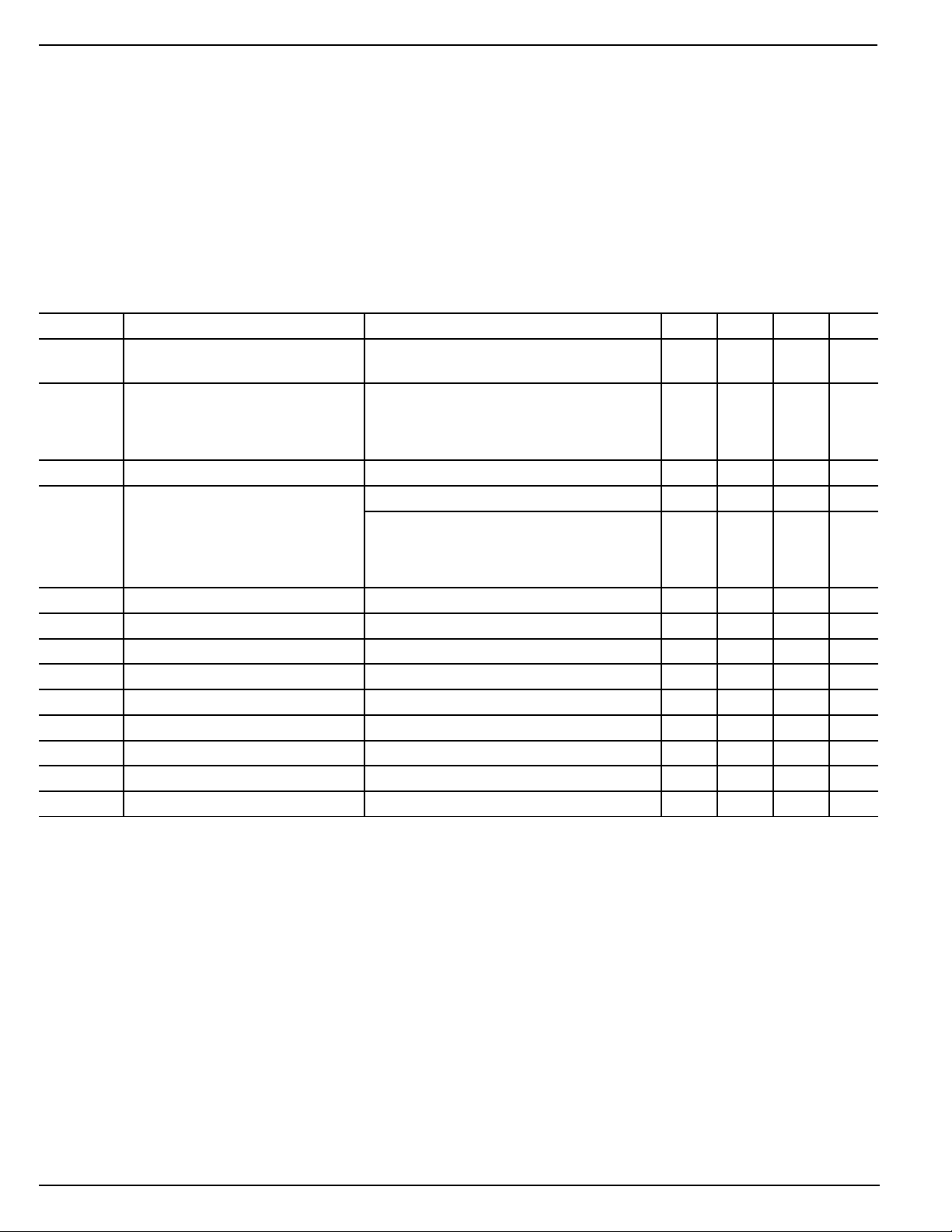
Note 3: See Figures 7, 8 and 9 for recommended operating conditions and limits. Absolute maximum for each output should be limited to 40mA.
Note 4: V
Note 5: AC input waveform specification for test purpose: tR ≤ 20ns, tF ≤ 20ns, f = 500kHz, 50% ±10% duty cycle.
Note 6: Clock input rise and fall times must not exceed 300ns.
Maximumbrightness control input current can be 2mA providing it complies with Note 3 and the junction temperature equation.
should be regulated by the user. See Figures 8 and 9 for allowable V
OUT
MAX
+ I
MIN
) ÷ 2.
OUT
vs. I
operation.
OUT
MM5450/5451 4 May 2000
Page 5
MM5450/5451 Micrel
Functional Description
The MM5450 and MM5451 were designed to drive either 4- or
5-digit alphanumeric LED displays with the added benefit of
requiring minimal interface with the display or data source.
Data is transferred serially via 2 signals; clock and serial data.
Data transfer without the added inconvenience of an external
load signal is accomplished by using a format of a leading “1”
followed by the allowed 35 data bits. These 35 data bits are
latched after the 36th has been transferred. This scheme
provides non multiplexed, direct drive to the LED display.
Characters currently displayed (thus, data output) changes
only if the serial data bits differ from those previously transferred.
Control of the output current for LED displays provides for the
display brightness. To prevent oscillations, a 1nF capacitor
should be connected to pin 19, brightness control.
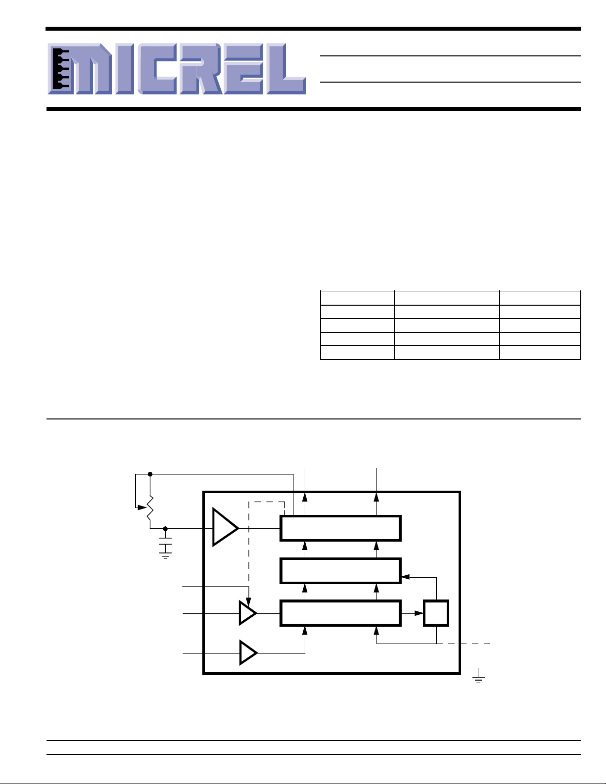
The block diagram is shown in Figure 1. For the MIC5450, the
DATA ENABLE is a metal option and is used instead of the
35th output. The output current is typically 20-times greater
that the current into pin 19, which is set by an external variable
resistor.
There is an external reset connection shown which is available
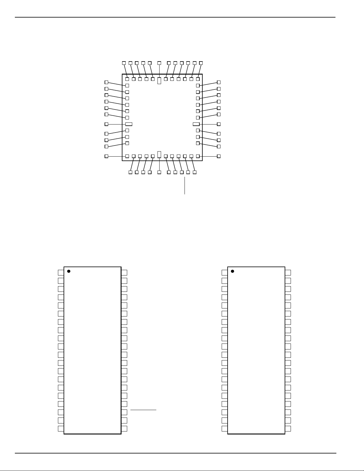
on unpackaged (die) only. Figure 2 illustrates the die pad
locations for bonding in “chip on board” applications.
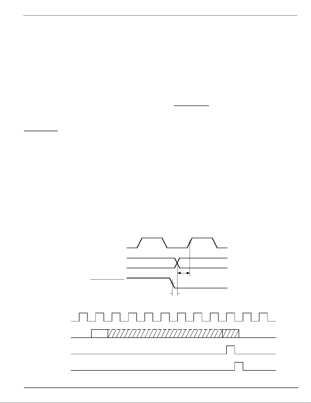
Figure 5 shows the input data format. A leading “1” is followed
by 35 bits of data. After the 36th had been transferred, a LOAD
signal is generated synchronously with the clock high state.
This loads the 35 bits of data into the latches. The low side of
the clock is used to generate a RESET signal which clears all
shift registers for the next set of data. All shift registers are
static master-slave, with no clear for the master portion of the
first register, allowing continuous operation.
There must be a complete set of 36 clocks or the shift registers
will not clear.
When the chip first powers ON, an internal power ON reset
signal is generated which resets all registers and all latches.
The START bit and the first clock return the chip to its normal
operation.
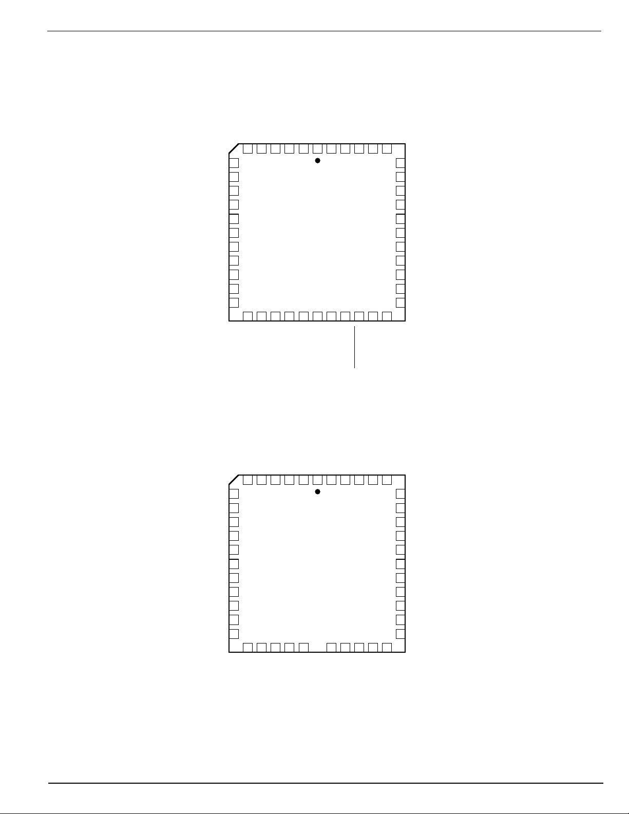
Figure 3 and 4 show the pin-out of the MIC5450 and MIC5451.
Bit 1 is the first bit following the start bit and it will appear on
pin 18. A logical “1” at the input will turn on the appropriate
LED.
Figure 5 shows the timing relationships between data, clock
and DATA ENABLE. A maximum clock frequency of 0.5MHz
is assumed.
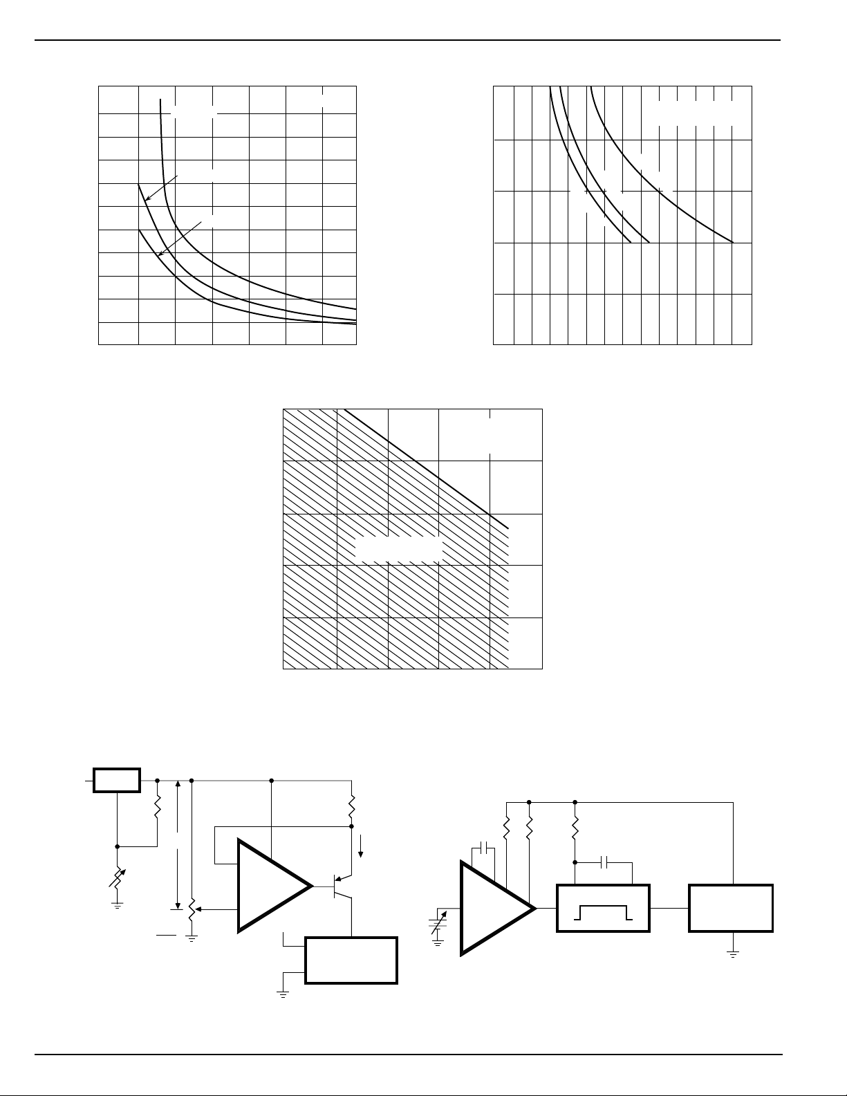
For applications where a lesser number of outputs are used,
it is possible to either increase the current per output, or
operate the part at higher than 1V V
equation can be used for calculations.
T
= (V
J
OUT
) (I
) (No. of segments) (124°C/W) + T
LED
. The following
OUT
A
where:
TJ = junction temperature + 150°C max
V
= the voltage at the LED driver outputs
OUT
I
= the LED current
LED
124°C/W = thermal resistance of the package
TA = ambient temperature
The above equation was used to plot Figures 7–9.
CLOCK
DATA
LOAD
(INTERNAL)
RESET
(INTERNAL)
CLOCK
DATA
300 nS MIN
DATA ENABLE
100 nS MIN
Figure 5.
1
START BIT 1 BIT 36
Figure 6. Input Data Format
BIT 35
36 37
May 2000 5 MM5450/5451
Page 6
MM5450/5451 Micrel
Typical Performance Characteristics
110
100
90
80
70
60
50
40
OUTPUT CURRENT (mA)
30
20
10
0
0 5 10 15 20 25 30
V = 1V
OUT
V = 1.5V
OUT
V = 2V
OUT
NUMBER OF SEGMENTS
Figure 7.
1.0
0.8
T = 85°C
A
2.5
T = 85°C
A
T = 150°C (MAX)
J
2.0
20 SEG
30 SEGM
1.5
OUT O
V (V )
1.0
0.5
34
0
0481216202428
34 SEGM
I (mA)
LED
M
Figure 8.
34 SEGMENTS
V = 1V
OUT
15 mA/SEGMENT
Typical Applications
240
Ω
5k
I19=
7V
∆V
∆V
1K
RAW DC
> 9 V
LM317
0.6
SAFE OPERATING
0.4
POWER DISSIPATION (W)
0.2
0
020406080
AREA
TEMPERATURE (°C)
Figure 9.
1k
I
19
–
LM324
+
5V
20
1
2N2907
PIN 19
MM5450
CD4046
(VCO)
5V
100
MM74HC123
10 µS
Q19
20
MM5450
1
Figure 11. Brightness Control Varying the Duty Cycle
Figure 10. Typical Application of Constant Current
Brightness Control
MM5450/5451 6 May 2000
Page 7
MM5450/5451 Micrel
Typical Applications
V
= 3.0V V
LED
LED DISPLAY
AM
FM
34
MM5450
DISPLAY DRIVER
ELECTRONIC
KEYBOARD
TUNING
CONTROLLER
SYNTHESIZER
STATION DETECT, ETC.
Figure 12. Basic Electronically Tuned Radio System
V
LED
V
LED
PLL
LED
= 3.0V
CLOCK IN
DATA IN
9–16 2–8, 40 32–39 24–31
MM5450
21 22 19 20 1 23 17
18
V
BRIGHTNESS
CONTROL
100k
DD
TYP.
Figure 13. Duplexing 8 Digits with One MM5450.
May 2000 7 MM5450/5451
Page 8
MM5450/5451 Micrel
Package Information
.020 MIN
20
21
.100 TYP
0.045
0.045
2.040
.018 TYP
TOP VIEW
0.050 TYP
NON-ACCUM
1
.100
40
.075
.150
.060 ± .002
.125 MIN
40-Pin Plastic DIP (N)
0.015
0.094
DETAIL A
0.104
.546 ±.010
105°/90°
.625±.025
.080 NOM
.030 NOM
.010
0.137 TYP
0.652
0.690 ±0.005
BOTTOM VIEW
0.125 DIA x 0.005 DEEP
4 PLCS (EJECTOR PIN)
44-Pin PLCC (V)
0.045
0.062 DIA
x
0.020 DEEP
DETAIL A
0.028
0.045
0.104
0.062
TYP
SIDE VIEW
0.172
0.030
TYP
0.035 R
±0.010
0.020 MIN
0.018
.610 ±.015
MICREL INC. 1849 FORTUNE DRIVE SAN JOSE, CA 95131 USA
TEL + 1 (408) 944-0800 FAX + 1 (408) 944-0970 WEB http://www.micrel.com
This information is believed to be accurate and reliable, however no responsibility is assumed by Micrel for its use nor for any infringement of patents or
other rights of third parties resulting from its use. No license is granted by implication or otherwise under any patent or patent right of Micrel Inc.
© 2000 Micrel Incorporated
MM5450/5451 8 May 2000
 Loading...