

查询MM54C221供应商
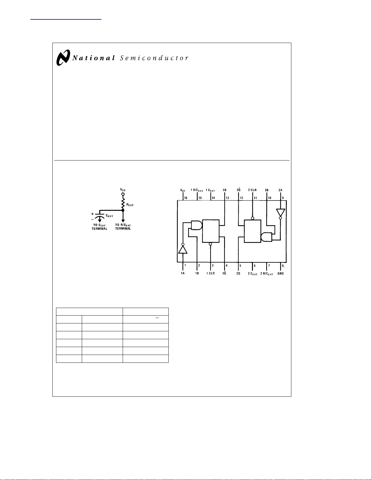
MM54C221/MM74C221 Dual Monostable Multivibrator
General Description
The MM54C221/MM74C221 dual monostable multivibrator
is a monolithic complementary MOS integrated circuit. Each
multivibrator features a negative-transition-triggered input
and a positive-transition-triggered input, either of which can
be used as an inhibit input, and a clear input.
Once fired, the output pulses are independent of further
transitions of the A and B inputs and are a function of the
external timing components C
width is stable over a wide range of temperature and V
Connection Diagrams
EXT
and R
. The pulse
EXT
Pulse stability will be limited by the accuracy of external
timing components. The pulse width is approximately defined by the relationship t
information and applications, see AN-138.
W(OUT)
&
C
EXTREXT
Features
Y
Wide supply voltage range 4.5V to 15V
Y
Guaranteed noise margin 1.0V
.
Y
CC
High noise immunity 0.45 VCC(typ.)
Y
Low power TTL compatibility fan out of 2
MM54C221/MM74C221 Dual Monostable Multivibrator
February 1988
. For further
driving 74L
Timing Component
TL/F/5904– 1
Truth Table
Inputs Outputs
Clear A B Q Q
LXXLH
XHXLH
XXLLH
HL
H
v
u
H Éß
Éß
Dual-In-Line Package
Top View
Order Number MM54C221 or MM74C221
e
H
High level
e
Low level
L
e
Transition from low to high
u
e
Transition from high to low
v
e
One high level pulse
É
e
One low level pulse
ß
e
Irrelevant
X
TL/F/5904– 2
C
1995 National Semiconductor Corporation RRD-B30M105/Printed in U. S. A.
TL/F/5904
Absolute Maximum Ratings (Note 1)
If Military/Aerospace specified devices are required,
please contact the National Semiconductor Sales
Office/Distributors for availability and specifications.
Voltage at Any Pin
Operating Temperature Range
MM54C221
MM74C221
Storage Temperature Range
b
0.3V to V
b
b
b
a
0.3V
CC
55§Ctoa125§C
40§Ctoa85§C
65§Ctoa150§C
Power Dissipation
Dual-In-Line 700 mW
Small Outline 500 mW
Operating V
Absolute Maximum V
R
EXT
Range 4.5V to 15V
CC
t
80 VCC(X)
CC
18V
Lead Temperature (Soldering, 10 seconds) 260§C
DC Electrical Characteristics Max/min limits apply across temperature range, unless otherwise noted
Symbol Parameter Conditions Min Typ Max Units
CMOS to CMOS
V
IN(1)
V
IN(0)
V
OUT(1)
V
OUT(0)
I
IN(1)
I
IN(0)
I
CC
I
CC
Logical ‘‘1’’ Input Voltage V
Logical ‘‘0’’ Input Voltage V
Logical ‘‘1’’ Output Voltage V
Logical ‘‘0’’ Output Voltage V
Logical ‘‘1’’ Input Current V
Logical ‘‘0’’ Input Current V
Supply Current (Standby) V
Supply Current V
(During Output Pulse) Q2
Leakage Current at R/C
EXT
Pin V
CMOS/LPTTL Interface
V
IN(1)
V
IN(0)
V
OUT(1)
V
OUT(0)
Logical ‘‘1’’ Input Voltage 54C V
Logical ‘‘0’’ Input Voltage 54C V
Logical ‘‘1’’ Output Voltage 54C V
Logical ‘‘0’’ Output Voltage 54C V
Output Drive (See 54C/74C Family Characteristics Data Sheet) (Short Circuit Current)
I
SOURCE
I
SOURCE
I
SINK
I
SINK
Output Source Current V
(P-Channel) T
Output Source Current V
(P-Channel) T
Output Sink Current V
(N-Channel) T
Output Sink Current V
(N-Channel) T
e
5V 3.5 V
CC
e
V
10V 8.0 V
CC
e
5V 1.5 V
CC
e
V
10V 2.0 V
CC
e
eb
5V, I
CC
e
V
10V, I
CC
e
5V, I
CC
e
V
10V, I
CC
e
15V, V
CC
e
15V, V
CC
e
15V, R
CC
e
Q1, Q2
e
15V, Q1eLogic ‘‘1’’,
CC
e
Logic ‘‘0’’
e
V
5V, Q1eLogic ‘‘1’’,
CC
e
Q2
Logic ‘‘0’’
e
15V, V
CC
CC
74C V
CC
CC
74C V
CC
CC
74C V
CC
CC
74C V
CC
e
5V
CC
e
25§C, V
A
e
10V
CC
e
25§C, V
A
e
5V
CC
e
25§C, V
A
e
10V
CC
e
25§C, V
A
10 mA 4.5 V
O
eb
10 mA 9.0 V
O
ea
10 mA 0.5 V
O
ea
10 mA1V
O
e
15V 0.005 1.0 mA
IN
e
0V
IN
e %
EXT
Logic ‘‘0’’ (Note 3)
,
(Figure 4)
(Figure 4)
e
5V 0.01 3.0 mA
CEXT
e
4.5V V
e
4.75V V
e
4.5V 0.8 V
e
4.75V 0.8 V
e
e
e
e
4.5V, I
4.75V, I
4.5V, I
4.75V, I
e
OUT
e
OUT
e
OUT
e
OUT
eb
360 mA 2.4 V
O
eb
360 mA 2.4 V
O
e
360 mA 0.4 V
O
e
360 mA 0.4 V
O
0V
0V
V
CC
V
CC
b
1.0
b
0.005 mA
0.05 300 mA
15 mA
2mA
b
1.5 V
CC
b
1.5 V
CC
b
1.75 mA
b
8mA
1.75 mA
8mA
2

AC Electrical Characteristics* T
e
A
25§C, C
e
50 pF, unless otherwise noted
L
Symbol Parameter Conditions Min Typ Max Units
t
pd A, B
t
pd CL
t
S
t
W(A, B)
t
W(CL)
t
W(OUT)
R
ON
Propagation Delay from Trigger V
Input (A, B) to Output Q, Q
Propagation Delay from Clear V
Input (CL) to Output Q, Q
Time Prior to Trigger Input (A, B) V
that Clear must be Set V
Trigger Input (A, B) Pulse Width V
Clear Input (CL) Pulse Width V
QorQOutput Pulse Width V
ON Resistance of Transistor V
between R/C
EXT
to C
EXT
e
5V 250 500 ns
CC
e
V
10V 120 250 ns
CC
e
5V 250 500 ns
CC
e
V
10V 120 250 ns
CC
e
5V 150 50 ns
CC
e
10V 60 20 ns
CC
e
5V 150 50 ns
CC
e
V
10V 70 30 ns
CC
e
5V 150 50 ns
CC
e
V
10V 70 30 ns
CC
e
5V, R
CC
e
C
EXT
e
V
10V, R
CC
e
C
EXT
e
V
15V, R
CC
e
C
EXT
e
V
5V, R
CC
e
C
EXT
e
V
10V, R
CC
e
C
EXT
e
V
15V, R
CC
e
C
EXT
e
V
5V, R
CC
e
C
EXT
e
V
10V, R
CC
e
C
EXT
e
V
15V, R
CC
e
C
EXT
e
5V (Note 4) 50 150 X
CC
e
V
10V (Note 4) 25 65 X
CC
e
V
15V (Note 4) 16.7 45 X
CC
EXT
0pF
0pF
0pF
EXT
1000 pF
1000 pF
1000 pF
EXT
0.1 mF
0.1 mF
0.1 mF
e
10k,
e
EXT
e
EXT
e
10k,
(Figure 1)
e
EXT
(Figure 1)
e
EXT
(Figure 1)
e
10k,
(Figure 2)
e
EXT
(Figure 2)
e
EXT
(Figure 2)
10k,
10k,
10k,
10k,
10k,
10k,
900 ns
350 ns
320 ns
9.0 10.6 12.2 ms
9.0 10 11 ms
8.9 9.8 10.8 ms
900 1020 1200 ms
900 1000 1100 ms
900 990 1100 ms
Output Duty Cycle Re10k, Ce1000 pF 90 %
e
R
10k, Ce0.1 mF90%
(Note 5)
C
IN
*AC Parameters are guaranteed by DC correlated testing.
Note 1: ‘‘Absolute Maximum Ratings’’ are those values beyond which the safety of the device cannot be guaranteed. Except for ‘‘Operating Temperature Range’’
they are not meant to imply that the devices should be operated at these limits. The table of ‘‘Electrical Characteristics’’ provides conditions for actual device
operation.
Note 2: Capacitance is guaranteed by periodic testing.
Note 3: In Standby (Q
Note 4: See AN-138 for detailed explanation R
Note 5: Maximum output duty cycle
Input Capacitance R/C
e
Logic ‘‘0’’) the power dissipated equals the leakage current plus VCC/R
e
R
EXT/REXT
.
ON
a
1000.
Input (Note 2) 15 25 pF
EXT
Any Other Input (Note 2) 5 pF
EXT
.
3

Typical Performance Characteristics
0% Point pulse width:
e
At V
CC
e
At V
CC
e
At V
CC
Percentage of units within
e
At V
CC
e
At V
CC
e
At V
CC
e
5V, T
W
e
10V, T
W
e
15V, T
W
5V, 90% of units
10V, 95% of units
15V, 98% of units
10.6 ms
10 ms
9.8 ms
a
4%:
FIGURE 1. Typical Distribution of Units for Output Pulse Width
FIGURE 2. Typical Distribution of Units for Output Pulse Width
FIGURE 3. Typical Variation in
Output Pulse Width vs Temperature
TL/F/5904– 5
TL/F/5904– 3
0% Point pulse width:
e
At V
CC
e
At V
CC
e
At V
CC
Percentage of units within
e
At V
CC
e
At V
CC
e
At V
CC
e
5V, T
10V, T
15V, T
5V, 95% of units
10V, 97% of units
15V, 98% of units
1020 ms
W
e
1000 ms
W
e
982 ms
W
TL/F/5904– 4
a
4%:
FIGURE 4. Typical Power Dissipation
per Package
TL/F/5904– 6
4

Switching Time Waveforms
e
e
t
t
20 ns
r
f
Physical Dimensions inches (millimeters)
TL/F/5904– 7
Ceramic Dual-In-Line Package (J)
Order Number MM54C221J or MM74C221C
NS Package Number J16A
5

Physical Dimensions inches (millimeters) (Continued)
Molded Dual-In-Line Package (N)
Order Number MM54C221N or MM74C221N
NS Package Number N16E
MM54C221/MM74C221 Dual Monostable Multivibrator
LIFE SUPPORT POLICY
NATIONAL’S PRODUCTS ARE NOT AUTHORIZED FOR USE AS CRITICAL COMPONENTS IN LIFE SUPPORT
DEVICES OR SYSTEMS WITHOUT THE EXPRESS WRITTEN APPROVAL OF THE PRESIDENT OF NATIONAL
SEMICONDUCTOR CORPORATION. As used herein:
1. Life support devices or systems are devices or 2. A critical component is any component of a life
systems which, (a) are intended for surgical implant support device or system whose failure to perform can
into the body, or (b) support or sustain life, and whose be reasonably expected to cause the failure of the life
failure to perform, when properly used in accordance support device or system, or to affect its safety or
with instructions for use provided in the labeling, can effectiveness.
be reasonably expected to result in a significant injury
to the user.
National Semiconductor National Semiconductor National Semiconductor National Semiconductor
Corporation Europe Hong Kong Ltd. Japan Ltd.
1111 West Bardin Road Fax: (
Arlington, TX 76017 Email: cnjwge@tevm2.nsc.com Ocean Centre, 5 Canton Rd. Fax: 81-043-299-2408
Tel: 1(800) 272-9959 Deutsch Tel: (
Fax: 1(800) 737-7018 English Tel: (
National does not assume any responsibility for use of any circuitry described, no circuit patent licenses are implied and National reserves the right at any time without notice to change said circuitry and specifications.
Fran3ais Tel: (
Italiano Tel: (
a
49) 0-180-530 85 86 13th Floor, Straight Block, Tel: 81-043-299-2309
a
49) 0-180-530 85 85 Tsimshatsui, Kowloon
a
49) 0-180-532 78 32 Hong Kong
a
49) 0-180-532 93 58 Tel: (852) 2737-1600
a
49) 0-180-534 16 80 Fax: (852) 2736-9960
 Loading...