

查询LP3931供应商
LP3931
Dual RGB LED Driver with High Current Boost DC-DC
Converter
LP3931 Dual RGB LED Driver with High Current Boost DC-DC Converter
August 2004
General Description
The LP3931 is a RGB LED driver with high current boost
DC-DC converter designed for portable wireless applications. It contains 2 sets of RGB LED drivers that are PWMdriven with programmable color, intensity and blinking patterns. They additionally feature a FLASH function to support
picture taking with camera-enabled cellular phones.
An efficient magnetic boost DC/DC converter provides the
required bias, operating from a single Li-Ion battery. The
DC/DC converter output voltage is user programmable for
adapting to different LED types and for efficiency optimization.
All functions are software controllable through the SPI interface and internal registers.
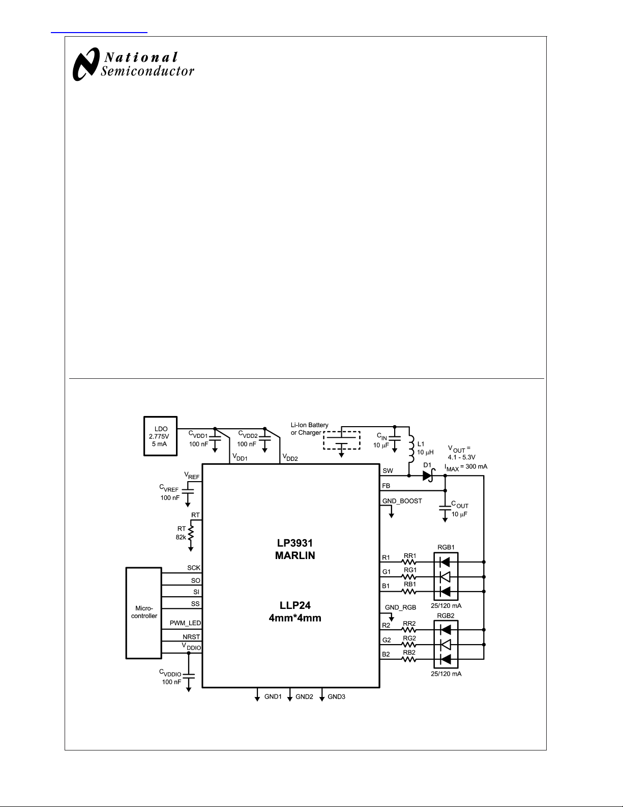
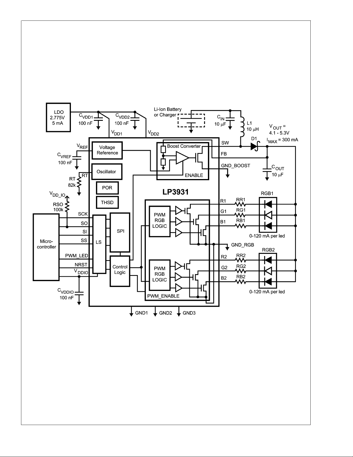
Typical Application
Features
n High Efficiency Programmable 300 mA Magnetic Boost
DC-DC converter
n 2 separately controlled PWM RGB LED drivers with
programmable color, brightness, turn on/off slopes and
blinking patterns
n FLASH function with up to 6 outputs, each up to
120 mA
n Functions software controlled through SPI interface
n Additional LED on/off and dimming hardware control
n Programmable low current Standby mode
n Low voltage digital interface down to 1.8V
n Space efficient 24-pin LLP package
Applications
n GSM Cellular Phones
n WCDMA, CDMA and CDMA2000 Phones
n PHS and PDC Cellular Phone
20117301
© 2004 National Semiconductor Corporation DS201173 www.national.com
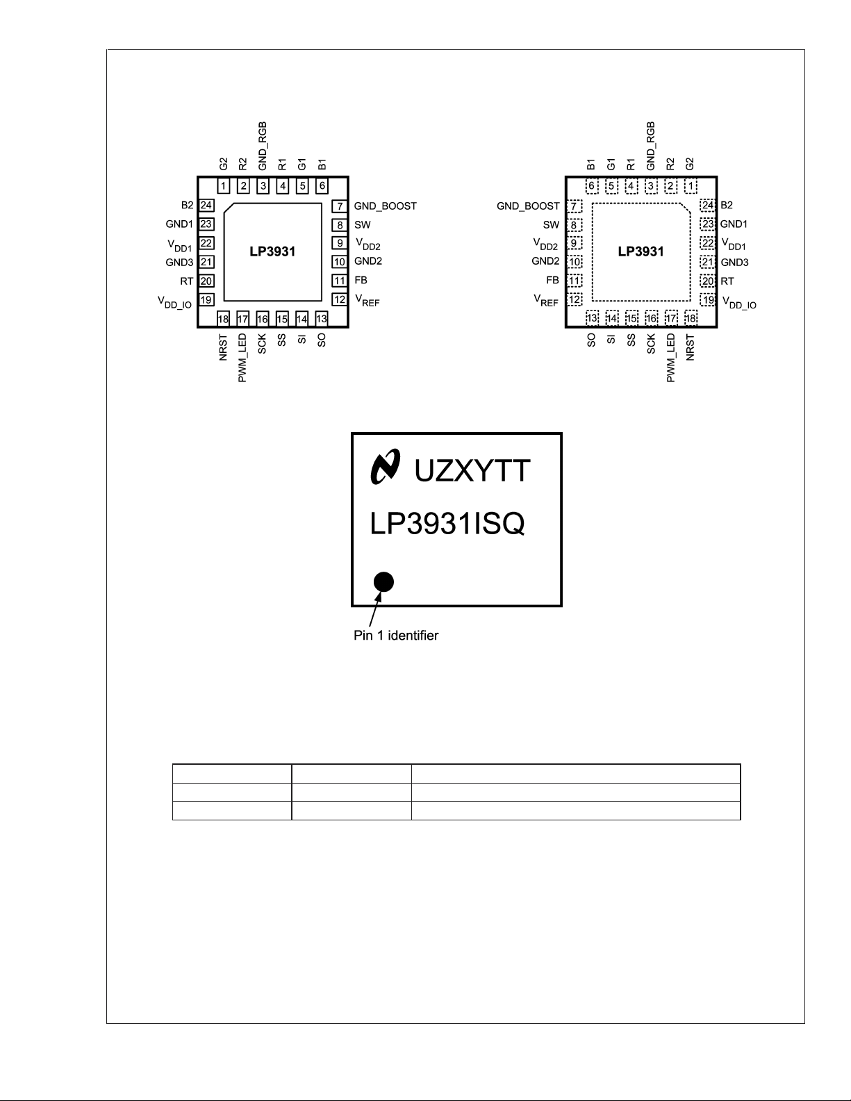
Connection Diagrams and Package Mark Information
LP3931
24-Lead LLP Package,4x4x0.8mm
NS Package Number NSQAL024
Bottom View
20117303
Top View
20117304
20117302
Package Mark — Top View
Note: The actual physical placement of the package marking will vary from part to part. The package marking “XY” designates
the date code. “UZ” and “TT” are NSC internal codes for die manufacturing and assembly traceability. Both will vary considerably.
Ordering Information
Order Number Package Marking Supplied As
LP3931ISQ LP3931ISQ 1000 units, Tape-and-Reel
LP3931ISQX LP3931ISQ 2500 units, Tape-and-Reel
www.national.com 2
Pin Description
Pin # Name Type Description
1 G2 Output Open Drain, Green LED2
2 R2 Output Open Drain, Red LED2
3 GND_RGB Ground RGB Driver Ground
4 R1 Output Open Drain, Red LED1
5 G1 Output Open Drain, Green LED1
6 B1 Output Open Drain, Blue LED1
7 GND_BOOST Ground Power Switch Ground
8 SW Output Open Drain, Boost Converter Power Switch
9V
DD2
10 GND2 Ground Ground
11 FB Input Boost Converter Feedback
12 V
REF
13 SO Logic Output SPI Serial Data Out
14 SI Logic Input SPI Serial Data Input
15 SS Logic Input SPI Slave Select
16 SCK Logic Input SPI Clock
17 PWM_LED Input LED Control for On/Off or PWM Dimming
18 NRST Logic Input Low Active Reset Input
19 V
DDIO
20 RT Input Oscillator Resistor
21 GND3 Ground Ground
22 V
DD1
23 GND1 Ground Ground
24 B2 Output Open Drain, Blue LED2
Power Supply Voltage for Internal Digital Circuits
Output Internal Reference Bypass Capacitor
Power Supply Voltage for Logic IO Signals
Power Supply Voltage for Internal Analog Circuits
LP3931
www.national.com3
Absolute Maximum Ratings (Notes 1,
2)
LP3931
If Military/Aerospace specified devices are required,
ESD Rating (Note 8)
Human Body Model: 2 kV
Machine Model: 200V
please contact the National Semiconductor Sales Office/
Distributors for availability and specifications.
V (SW, FB, R1- 2, G1-2,
B1-2) pins:
Voltage to GND (Notes 3, 4) −0.3V to +7.2V
V
DD1,VDD2,VDD_IO
Voltage on Logic Pins –0.3V to V
−0.3V to +6.0V
DD_IO
+0.3V, with 6.0V max
I (R1, G1, B1, R2, G2, B2)
(Note 5) 150 mA
I(V
)10µA
REF
Continuous Power Dissipation
(Note 6) Internally Limited
Junction Temperature (T
) 125˚C
J-MAX
Operating Ratings (Notes 1, 2)
V (SW, FB, R1-2, G1-2, B1-2) 3.0V to 6.0V
V
DD1,VDD2
V
DD_IO
(Note 4) 2.65V to 2.9V
1.8V to V
Recommended Load Current 0 mA to 300 mA
Junction Temperature (T
Ambient Temperature (T
) Range −40˚C to +125˚C
J
) Range
A
(Note 9) −40˚C to +85˚C
Thermal Properties
Junction-to-Ambient Thermal Resistance (θJA),
SQA24A Package (Note 10) 39˚C/W
Storage Temperature Range −65˚C to +150˚C
Maximum Lead Temperature
(Reflow soldering, 3 times)
(Note 7) 240˚C
Electrical Characteristics (Notes 2, 11)
Limits in standard typeface are for TJ= 25˚C. Limits in boldface type apply over the operating ambient temperature range
(−40˚C ≤ T
=V
DD2=VDDIO
(Note 12).
Symbol Parameter Condition Min Typ Max Units
I
DD
I
DD_IO
V
REF
Note 1: Absolute Maximum Ratings indicate limits beyond which damage to the component may occur. Operating Ratings are conditions under which operation of
the device is guaranteed. Operating Ratings do not imply guaranteed performance limits. For guaranteed performance limits and associated test conditions, see the
Electrical Characteristics tables.
Note 2: All voltages are with respect to the potential at the GND pins (GND1-3, GND_BOOST, GND_RGB).
Note 3: Battery/Charger voltage should be above 6V no more than 10% of the operational lifetime.
Note 4: Voltage tolerance of LP3931 above 6.0V relies on fact that V
(ON) at all conditions, National Semiconductor does not guarantee any parameters or reliability for this device.
Note 5: The total load current of the boost converter should be limited to 300 mA.
Note 6: Internal thermal shutdown circuitry protects the device from permanent damage. Thermal shutdown engages at T
140˚C (typ.).
Note 7: For detailed package and soldering specifications and information, please refer to National Semiconductor Application Note 1187: Leadless Leadframe
Package (LLP).
Note 8: The Human body model is a 100 pF capacitor discharged through a 1.5 kΩ resistor into each pin. The machine model is a 200 pF capacitor discharged
directly into each pin. MIL-STD-883 3015.7.
≤ +85˚C). Unless otherwise noted, specifications apply to the LP3931 Typical Application Circuit (pg. 1) with: V
J
= 2.775V, C
VDD1=CVDD2=CVDDIO
Standby Supply Current
(V
DD1
and V
DD2
current)
No-Load Supply Current
(V
DD1
and V
current, boost off)
DD2
= 0.1 µF, C
OUT=CIN
NSTBY = L (register)
SCK, SS, SI, NRST = H
NSTBY = H (reg.)
EN_BOOST = L (reg.)
= 10 µF, C
= 0.1 µF, L1= 10 µH, RT= 82k
VREF
1 5 µA
170 250 µA
SCK, SS, SI, NRST = H
Full Load Supply Current
(V
DD1
and V
current, boost on)
DD2
NSTBY = H (reg.)
EN_BOOST = H (reg.)
SCK, SS, SI, NRST = H
1mA
All Outputs Active
V
Standby Supply Current NSTBY = L (reg.)
DD_IO
SCK, SS, SI, NRST = H
V
Supply Current 1 MHz SCK Frequency
DD_IO
=50pFatSOPin
C
L
Reference Voltage (Note 13) I (V
REF
Test Purposes Only
DD1
) ≤ 1 nA,
and V
(2.775V) are available (ON) at all conditions. If V
DD2
1.205
−2
1µA
20 µA
1.23 1.255
+2
and V
DD1
= 160˚C (typ.) and disengages at TJ=
J
are not available
DD2
DD1,2
DD1
V
%
www.national.com 4
Electrical Characteristics (Notes 2, 11) (Continued)
Note 9: In applications where high power dissipation and/or poor package thermal resistance is present, the maximum ambient temperature may have to be
derated. Maximum ambient temperature (T
dissipation of the device in the application (P
following equation: T
Note 10: Junction-to-ambient thermal resistance is highly application and board-layout dependent. In applications where high maximum power dissipation exists,
special care must be paid to thermal dissipation issues in board design.
Note 11: Min and Max limits are guaranteed by design, test, or statistical analysis. Typical numbers are not guaranteed, but do represent the most likely norm.
Note 12: Low-ESR Surface-Mount Ceramic Capacitors (MLCCs) are used in setting electrical characteristics.
Note 13: V
A-MAX=TJ-MAX-OP
pin (Bandgap reference output) is for internal use only. A capacitor should always be placed between V
REF
) is dependent on the maximum operating junction temperature (T
A-MAX
), and the junction-to ambient thermal resistance of the part/package in the application (θJA), as given by the
D-MAX
−(θJAxP
D-MAX
).
= 125˚C), the maximum power
J-MAX-OP
and GND1.
REF
Block Diagram
LP3931
LP3931 Block Diagram
20117305
www.national.com5
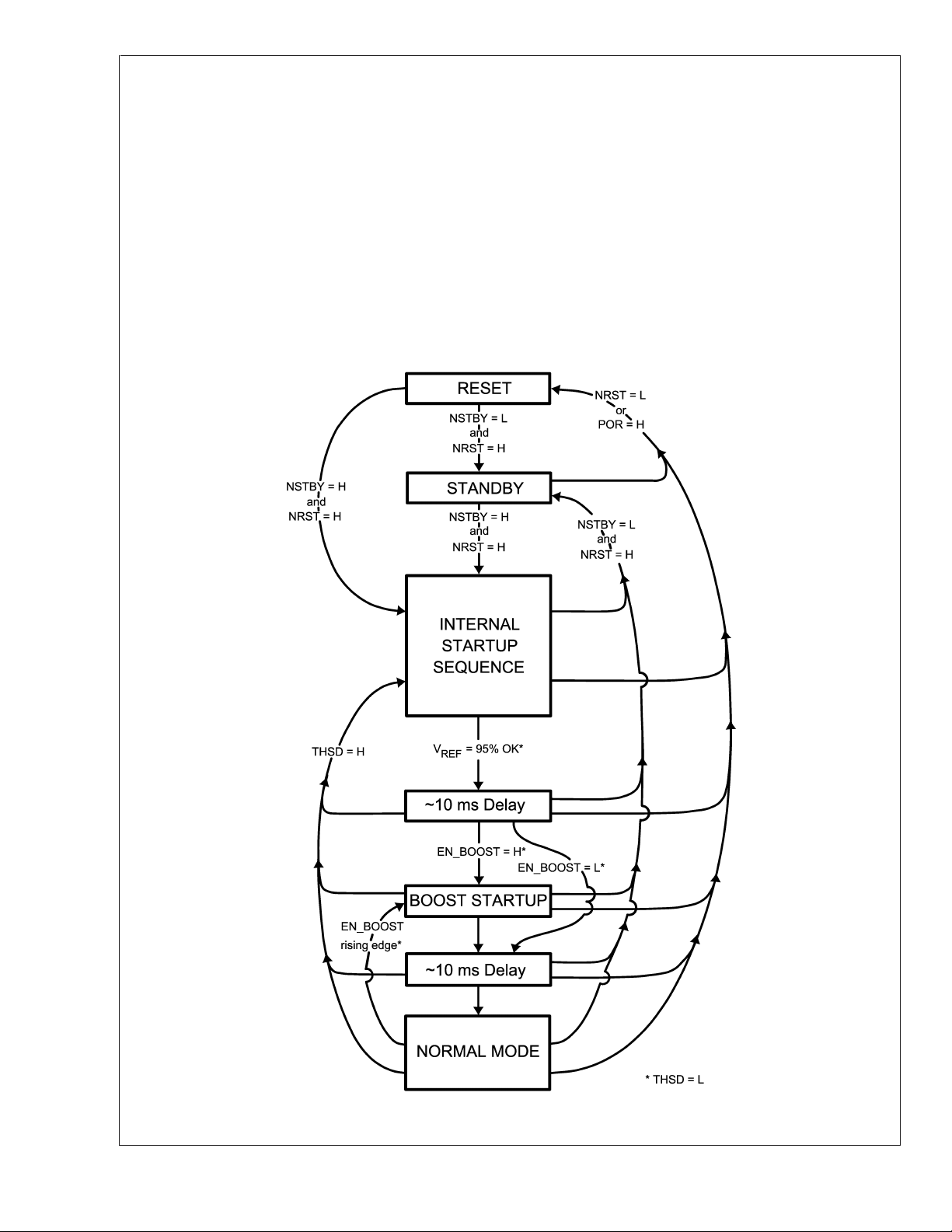
Modes of Operation
RESET: In the RESET mode all the internal registers are reset to the default values (Boost output register 3Fh
LP3931
STANDBY: The STANDBY mode is entered if the register bit NSTBY is LOW and Reset is not active. This is the low
STARTUP: INTERNAL STARTUP SEQUENCE powers up all the needed internal blocks (V
BOOST STARTUP: Soft start for boost output is generated in the BOOST STARTUP mode. In this mode the boost output is
NORMAL: During NORMAL mode the user controls the chip using the Control Registers. The registers can be written
(5.0V), all other registers 00h). Reset is entered always if input NRST is LOW or internal Power On Reset
is active.
power consumption mode, when all circuit functions are disabled. Registers can be written in this mode and
the control bits are effective immediately after power up.
, Bias, Oscillator etc.).
REF
To ensure the correct oscillator initialization, a 10 ms delay is generated by the internal state-machine.
Thermal shutdown (THSD) disables the chip operation and Startup mode is entered until no thermal
shutdown event is present.
raised in PFM mode during the 10 ms delay generated by the state-machine. The Boost startup is entered
from Internal Startup Sequence if EN_BOOST is HIGH or from Normal mode when EN_BOOST is written
HIGH.
in any sequence and any number of bits can be altered in a register in one write.
www.national.com 6
20117306
 Loading...