

LP3905
Power Management Unit For Low Power Handheld
Applications
LP3905 Power Management Unit For Low Power Handheld Applications
August 2006
General Description
LP3905 is a multi-functional Power Management Unit,
optimized for low power handheld applications. This device
integrates two 600mA DC/DC buck regulators and two
150mA linear regulators. Fixed and adjustable buck output
versions are available. The LP3905 additionally features two
enable pins for the device output control and is offered in an
LLP package.
Features
n Two buck regulators for powering high current processor
functions or peripheral devices
n Two linear regulators for powering internal processor
functions and I/Os
n One enable pin for Buck1 and Linear Regulators1&2
n Separate enable pin for Buck2
n Thermal and current overload protection
n Small 14–Pin LLP package (4mm x 4mm x 0.8mm)
Applications
n Baseband Processors
n Peripheral Processor (Video, Audio)
n I/O Power
n FPGA Power
Key Specifications
Buck Regulators
n Fixed and adjustable voltage options, range 1.0V to
3.3V *
n Up to 90% Efficiency
n Auto-switching PFM-PWM mode and fixed PWM mode
n 2MHz PWM fixed switching frequency (Typ)
n 600mA output current
±
n
4% output voltage accuracy over temp.
n Internal softstart
n 2.2µH inductor, 10µF Input and 10µF output Caps
Linear Regulators
n Output options in the range 1.5V to 3.3V *
n 13.5µV
n PSRR - 70dB
±
n
3% output voltage accuracy over full line and load
regulation
n 0mA to 150mA output current
n C
in
C
in
80mV Dropout voltage
* Fixed output voltage devices can be customized to fit
system requirements. Please contact National Semiconductor Sales Office.
output voltage noise
rms
@
= 1.0µF, C
= 1.0µF, C
out
out
1kHz
= 0.47µF for 100mA O/P
= 1.0µF for 150mA O/P
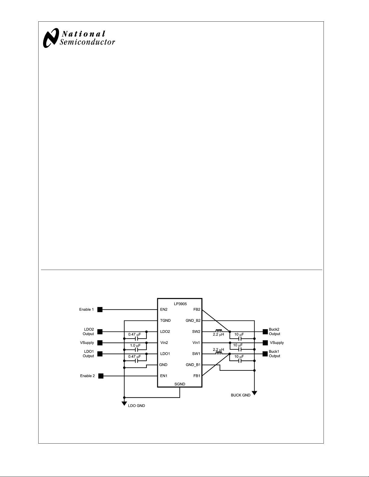
Typical Application Circuit
20152901
FIGURE 1. Typical Application Circuit – 14 Pin LLP Package
© 2006 National Semiconductor Corporation DS201529 www.national.com
Block Diagram
LP3905
Connection Diagram
20152902
FIGURE 2. Simplified Functional Diagram
20152907
FIGURE 3. 14 Pin LLP Package
www.national.com 2
Connection Diagram (Continued)
Pin Descriptions
Pin # Name Description
1 EN2 Enable Pin for Buck2
2 TGND Ground Pin
3 LDO2 LDO2 Output Pin
4 VIN2 Input Power Terminal to LDO1 & 2
5 LDO1 LDO1 Output Pin
6 GND LDO1 & 2 Ground Pin
7 EN1 Enable Pin for Buck1 and LDO1&2
8 FB1 Buck1 Feedback Pin
9 GND_B1 Buck1 Ground Pin
10 SW1 Buck1 Switch Pin
11 VIN1 Input Power Terminal to Buck1 & 2
12 SW2 Buck2 Switch Pin
13 GND_B2 Buck2 Ground Pin
14 FB2 Buck2 Feedback Pin
DAP SGND Die Attach Pad (DAP)
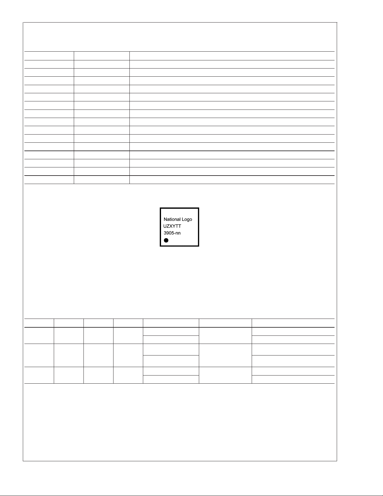
Package Marking Diagram
LP3905
20152905
The physical placement of the package marking will vary from part to part.
•
Date Code - UZXYTT format. ’U’ - Wafer fab code; ’Z’ - assembly site code; ’XY’ 2 digit date code; ’TT’ die run code
•
See National Web site for more info - http://www.national.com/quality/marking_conventions.html
•
FIGURE 4. LP3905 14 Pin LLP Package Marking
NS package number SDA14B
Ordering Information
Buck 1 [V] Buck 2 [V] LDO 1 [V] LDO 2 [V] Order Number Package Marking Supplied As
1.2 1.875 2.8 2.8 LP3905SD-00
LP3905SDX-00 4500 units, Tape-and-Reel
1.2 Fixed
PWM
ADJ ADJ 3.0 2.8 LP3905SD-A3
1.875
Fixed
PWM
2.8 2.8 LP3905SD-30
LP3905SDX-30 4500 units, Tape-and-Reel
LP3905SDX-A3 4500 units, Tape-and-Reel
3905-00
3905-30
3905-A3
1000 units, Tape-and-Reel
1000 units, Tape-and-Reel
1000 units, Tape-and-Reel
www.national.com3
Absolute Maximum Ratings (Note 1)
If Military/Aerospace specified devices are required,
LP3905
please contact the National Semiconductor Sales Office/
Distributors for availability and specifications.
1,VIN2 −0.2V to 6.0V
V
IN
FB1, FB2, EN1,EN2 (GND−0.2V) to
+ 0.2V) to 6.0V
(V
IN
Continuous Power Dissipation
(Note 3)
Junction Temperature (T
) +150˚C
J-MAX
Storage Temperature Range −65˚C to +150˚C
Maximum Lead Temperature
(Soldering, 10 sec.)
Internally Limited
(max)
260˚C
Operating Ratings (Notes 1, 2)
V
1 (Buck1&2 Input
IN
Voltage),V
Voltage) (Note 7)
Recommended Load Current
(Buck)
Recommended Load Current
(LDO)
Junction Temperature (T
Range
Ambient Temperature (T
Range (Note 5)
2 (LDO1&2 Input
IN
0mA to 100mA with
0mA to 150mA with
)
J
)
A
0mA to 600 mA
0.47uF O/P cap
1.0uF O/P cap
−40˚C to +125˚C
−40˚C to +85˚C
ESD Rating (Note 4)
Human Body Model: 2.5kV
Thermal Properties
Junction-to-Ambient
Thermal Resistance (θ
)
JA
SDA14B package(Note 6)
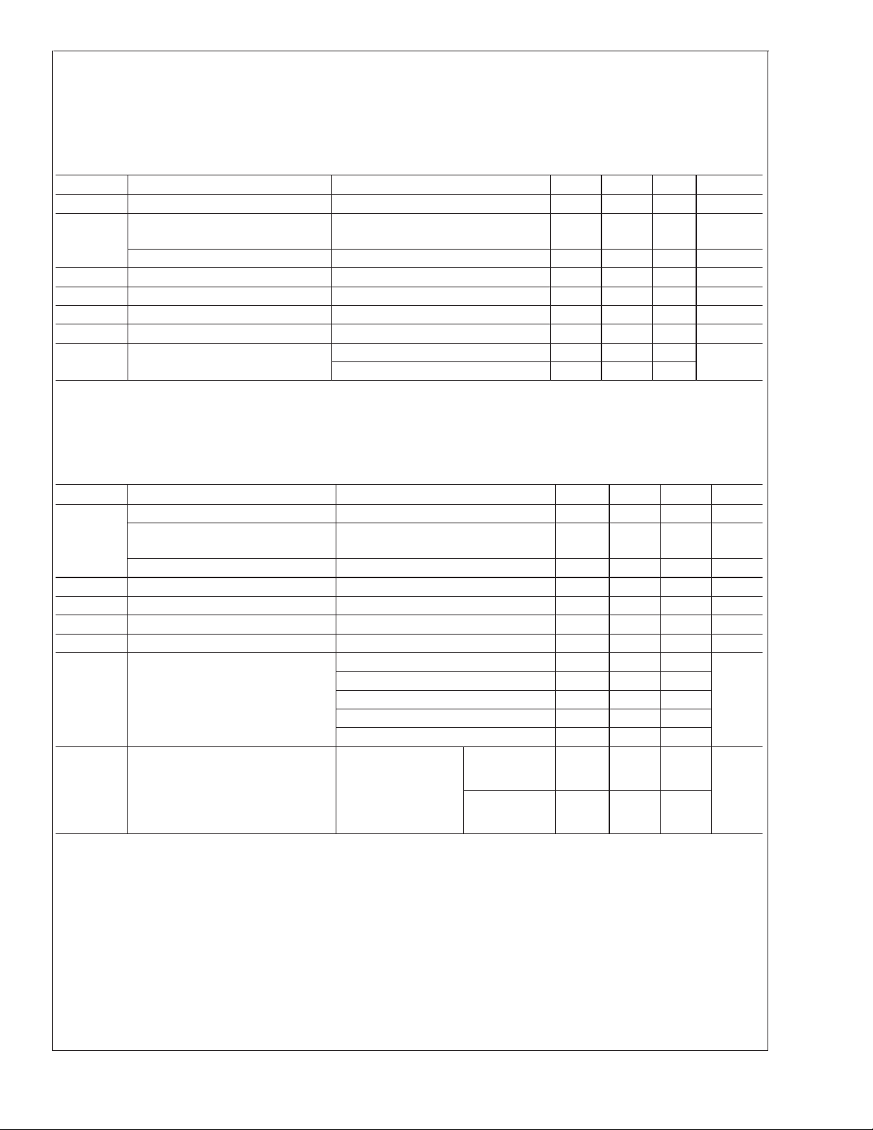
General Electrical Characteristics (Notes 2, 8, 9)
Limits in standard typeface are for TJ= 25˚C. Limits in boldface type apply over the full junction temperature range (−40˚C ≤
≤ +125˚C). Unless otherwise noted, specifications apply to the LP3905 Typical Application Circuit (Figure. 1)
T
J
Symbol Parameter Condition Min Typ Max Units
Login Input Thresholds
V
IN
I
Q
V
IH
V
IL
I
EN
V
UVLO-R
T
SHUTDOWN
Input Voltage Range 3 5.5 V
Shutdown Supply Current All Circuits OFF except for POR and
6.5 10.0 µA
UVLO
No load Supply Current (Note 15) LDO1 & 2 and Buck1&2on 140 250
( PWM only versions ) LDO1 & 2
7 10.0 mA
and Buck1&2on
Logic High Input VIN= 3.0V to 5.5V 1.2 V
Logic Low Input VIN= 3.0V to 5.5V 0.4 V
Enable (EN1,2) Input Current
(Note 14)
EN1/EN2 = 5.5V and VIN= 5.5V 2.1 5 8.5 µA
EN1/EN2 = 0V and V
= 5.5V 0.001 0.1 µA
IN
Battery Under Voltage Lock-Out VINRising 2.7 3.1 V
Thermal Shutdown (Note 15) Temperature 160
Hysteresis 20
3V to 5.5V
o
C/W
37.3
˚C
www.national.com 4
General Electrical Characteristics (Notes 2, 8, 9) (Continued)
Buck Regulator Electrical Characteristics
Buck1&2have a current rating of I
(Buck1)
= Vnom1 , V
OUT(Buck2)
= Vnom2 and CIN=C
type apply over the full junction temperature range (−40˚C ≤ T
LP3905 Typical Application Circuit (Figure. 1) (Notes 2, 8)
Symbol Parameter Condition Min Typ Max Units
V
FB
V
OUT
Feedback Voltage (Note 16) -4 +4 %
Line Regulation 3.0V ≤ VIN≤ 5.5V
Load Regulation 100 mA ≤ I
R
DSON (P)
R
DSON (N)
I
LIM
F
OSC
Pin-Pin Resistance for PFET VIN=VGS= 3.6V 380 500 mΩ
Pin-Pin Resistance for NFET VIN=VGS= 3.6V (Note 15) 250 400 mΩ
Switch Peak Current Limit Open Loop 650 1000 1220 mA
Internal Oscillator Frequency PWM Mode 2 MHz
η Efficiency IOUT = 5mA, PFM mode (Note 15) 88 %
= 600mA. Unless otherwise specified, limits are set with VIN=V
max
=10µF. Limits in standard typeface are for TJ= 25˚C. Limits in boldface
OUT
I
O
= 1mA
≤ +125˚C). Unless otherwise noted, specifications apply to the
J
≤ 600mA 0.002 %/mA
O
IOUT = 300mA, PWM mode (Note 15) 90
= 3.8V, V
EN1/2
OUT
0.045 %/V
LDO Regulator Electrical Characteristics
The linear regulators have a current rating of I
Unless otherwise specified, limits are set with V
standard typeface are for T
= 25˚C. Limits in boldface type apply over the full junction temperature range (−40˚C ≤ TJ≤
J
+125˚C). Unless otherwise noted, specifications apply to the LP3905 Typical Application Circuit (Figure. 1)(Notes 2, 8)
Symbol Parameter Conditions Min Typ Max Units
∆V
OUT
Output Voltage Tolerance Over Full Line and Load Regulation −3 3 %
Line Regulation Error V
Load Regulation Error I
I
LOAD
V
I
SC
I
OUT
DO
Load Current (Notes 11, 15) 0 mA
Dropout Voltage I
Short Circuit Current Limit (Note 13) 300 500 mA
Maximum Output Current C
PSRR Power Supply Rejection Ratio
(Note 15)
e
n
Output Noise Voltage
(Note 15)
= 150mA with C
max
= 3.8V, V
IN
= 3.8V to 5.5V,
IN
= 1mA
I
OUT
= 1 mA to 100mA 0.003 %/mA
OUT
= 100mA 80 150 mV
OUT
= 1.0µF 150 mA
OUT
f = 100Hz, I
f = 1kHz, I
f = 10kHz, I
f = 50kHz, I
f = 100kHz, I
BW = 10Hz to
100kHz, V
Buck1 Turned ON
with I
LOAD
Buck2 Turned OFF
= 1.0µF. A 100mA rating applies with C
OUT
= 3.8V, CIN= 1µF, C
EN1/2
= 100mA 90
OUT
= 100mA 90
OUT
= 100mA 60
OUT
= 100mA 35
OUT
= 100mA 25
OUT
= 1mA
I
OUT
= 4.2V
IN
I
= 100mA 15.5
= 0mA,
OUT
OUT
= 0.47µF, I
= 0.47µF.
OUT
= 1.0mA. Limits in
OUT
0.05 %/V
µV
13.5
LP3905
-
dB
RMS
www.national.com5

General Electrical Characteristics (Notes 2, 8, 9) (Continued)
LP3905
LDO Regulator Electrical Characteristics (Continued)
The linear regulators have a current rating of I
Unless otherwise specified, limits are set with V
standard typeface are for T
= 25˚C. Limits in boldface type apply over the full junction temperature range (−40˚C ≤ TJ≤
J
+125˚C). Unless otherwise noted, specifications apply to the LP3905 Typical Application Circuit (Figure. 1)(Notes 2, 8)
Symbol Parameter Conditions Min Typ Max Units
Transient Characteristics (Note 15)
∆V
OUT
Line Transient (Note 15) VIN=(V
Load Transient (Note 15) I
Overshoot on Startup (Note 15) 20 mV
= 150mA with C
max
= 3.8V, V
IN
(V
OUT(NOM
mA
=(V
V
IN
(V
OUT(NOM
1mA
= 1mA to 100mA in 10µs -70
OUT
I
= 100mA to 1mA in 10µs 30
OUT
I
= 1mA to 150mA in 10µs
OUT
= 1.0µF
C
OUT
I
= 150mA to 1mA in 10µs
OUT
= 1.0µF
C
OUT
= 1.0µF. A 100mA rating applies with C
OUT
= 3.8V, CIN= 1µF, C
EN1/2
OUT(NOM
) + 1.0V) to
) + 1.6V) in 10µs, I
OUT(NOM
) + 1.6V) to
) + 1.0V) in 10µs, I
OUT
OUT
OUT
=1
=
= 0.47µF, I
6
-100
OUT
= 1.0mA. Limits in
OUT
= 0.47µF.
mV
6
mV
35
Electrical Characteristics Notes
Note 1: Absolute Maximum Ratings indicate limits beyond which damage to the component may occur. Operating Ratings are conditions under which operation of
the device is guaranteed. Operating Ratings do not imply guaranteed performance limits. For guaranteed performance limits and associated test conditions, see the
Electrical Characteristics tables.
Note 2: All voltages are with respect to the potential at the GND pin.
Note 3: Internal thermal shutdown circuitry protects the device from permanent damage.
Note 4: The Human body model is a 100 pF capacitor discharged through a 1.5 kΩ resistor into each pin. MIL-STD-883 3015.7
Note 5: In Applications where high power dissipation and/or poor package resistance is present, the maximum ambient temperature may have to be derated.
Maximum ambient temperature (T
the application (P
(θ
JAxPD-MAX
Note 6: Junction to ambient thermal resistance is highly dependent on board layout, PCB material environmental conditions and applications. In applications where
high power dissipation exists, special care must be given to thermal dissipation issues in board design. The use of thermal vias under the pad may be required. For
more on these topics, please refer to the Application Note: AN-1187: Leadless leadframe Package (LLP).
Note 7: V
Note 8: Min and Max limits are guaranteed by design, test or statistical analysis. Typical numbers are not guaranteed, but do represent the most likely norm.
Note 9: The parameters in the electrical characteristic table are tested at V
to datasheet curves.
Note 10: C
Note 11: The device maintains a stable, regulated output voltage without a load.
Note 12: Dropout voltage is the voltage difference between the input and the output at which the output voltage drops to 100 mV below its nominal value.
Note 13: Short Circuit Current is measured with V
Note 14: There isa1MΩ resistor between EN1,EN2 and ground on the device.
Note 15: This specification is guaranteed by design.
Note 16: For the adjustable version, feedback resistor values should be chosen for the divider network to ensure that at the desired output voltage the feedback
pin is at 0.5V. See Buck Converter Applications Information.
IN1
IN,COUT
) and the junction to ambient thermal resistance of the package (θJA) in the application, as given by the following equation:T
D-MAX
).
and V
should be tied together at all times for proper Power Up
IN2
: Low-ESR Surface-Mount Ceramic Capacitors (MLCCs) used in setting electrical characteristics.
) is dependent on the maximum operating junction temperature (T
A-MAX
= 3.8V unless otherwise specified. For performance over the input voltage range refer
IN
pulled to 0v and VINworst case = 5,5V.
OUT
), the maximum power dissipation of the device in
J-MAX
A-MAX=TJ-MAX
−
www.national.com 6

Typical Application Circuit
FIGURE 5. Typical Application Circuit For Adjustable Device
LP3905
20152911
Functional Description
POWER UP/DOWN PROCEDURE
The LP3905 Bucks and LDOs are powered UP/DOWN with
2 control pins, EN1 and EN2. In order for the enable pins to
operate, V
than V
UVLO_R
IN1
and V
should be set to a voltage level higher
IN2
(specified in electrical characteristic). Once
enabled, EN1 will turn on Buck1, LDO1 and LDO2. EN2 can
independently be used to enable Buck2. Figure 6 illustrates
the power UP/DOWN timing sequence of the LP3905 blocks
for V
≥ V
EN
(enable) and VEN≤V
IH (min)
IL (max)
(disable).
Both linear regulators have active pulldowns when the outputs are disabled.
20152904
EN1 and EN2 can be controlled fully independently.
LDOs will be turned on only after Buck1 is powered up. LDOs are powered on simultaneously.
In case EN1 and EN2 are enabled at the same time, power up of Buck2 is delayed by 50µs in order to minimize the inrush current
from the battery.
When EN1 and EN2 are disabled, the relevant output voltages are turned off.
FIGURE 6. LP3905 Power UP/DOWN Timing Sequence
www.national.com7

Functional Description (Continued)
LP3905
DC/DC BUCK REGULATORS
The LP3905 Buck regulators are high efficiency step down
DC-DC switching converters used for delivering a constant
voltage from either a single Li-Ion or three cell NiMH/NiCd
battery to portable devices such as cell phones and PDAs.
Using a voltage mode architecture with synchronous rectification, the Buck Regulators have the ability to deliver up to
600 mA depending on the input voltage, output voltage,
ambient temperature and the inductor chosen.
There are three modes of operation depending on the current required - PWM, PFM, and shutdown. The standard
device operates in PWM mode at load currents of approximately 80 mA or higher, having voltage tolerance of
with 90% efficiency or better. Lighter load currents cause the
device to automatically switch into PFM for reduced current
BUCK CONVERTER BLOCK DIAGRAM
consumption and a longer battery life. Shutdown mode turns
off the device, offering the lowest current consumption . A
fixed mode device is also available which is fixed in PWM
mode for both low and high load currents.
An adjustable voltage version is also avalable for which the
output voltage can be selected by using two external resistors at each of the two buck outputs.
Additional features include soft-start, under voltage protection, current overload protection, and thermal shutdown protection.
The part uses an internal reference voltage of 0.5V. It is
±
4%
recommended to keep the part in shutdown until the input
voltage is 3V or higher.
FIGURE 7. Simplified Functional Diagram
CIRCUIT OPERATION
The LP3905 Buck regulators operate as follows. During the
first portion of each switching cycle, the control block in the
LP3905 turns on the internal PFET switch. This allows current to flow from the input through the inductor to the output
filter capacitor and load. The inductor limits the current to a
ramp with a slope of (V
IN–VOUT
)/L, by storing energy in a
magnetic field.
During the second portion of each cycle, the controller turns
the PFET switch off, blocking current flow from the input, and
then turns the NFET synchronous rectifier on. The inductor
www.national.com 8
20152918
draws current from ground through the NFET to the output
filter capacitor and load, which ramps the inductor current
down with a slope of - V
OUT
/L.
The output filter stores charge when the inductor current is
high, and releases it when inductor current is low, smoothing
the voltage across the load.
The output voltage is regulated by modulating the PFET
switch on time to control the average current sent to the load.
The effect is identical to sending a duty-cycle modulated
rectangular wave formed by the switch and synchronous

Functional Description (Continued)
rectifier at the SW pin to a low-pass filter formed by the
inductor and output filter capacitor. The output voltage is
equal to the average voltage at the SW pin.
PWM OPERATION
During PWM operation the converters operate as a voltagemode controllers with input voltage feed forward. This allows
the converters to achieve good load and line regulation. The
DC gain of the power stage is proportional to the input
voltage. To eliminate this dependence, feed forward inversely proportional to the input voltage is introduced.
While in PWM (Pulse Width Modulation) mode, the output
voltage is regulated by switching at a constant frequency
and then modulating the energy per cycle to control power to
the load. At the beginning of each clock cycle the PFET
switch is turned on and the inductor current ramps up until
the comparator trips and the control logic turns off the switch.
The current limit comparator can also turn off the switch in
case the current limit of the PFET is exceeded. Then the
NFET switch is turned on and the inductor current ramps
down. The next cycle is initiated by the clock turning off the
NFET and turning on the PFET.
PFM OPERATION
At very light loads, the converters enters PFM mode and
operate with reduced switching frequency and supply current
to maintain high efficiency.
The Bucks will automatically transition into PFM mode when
either of two conditions occurs for a duration of 32 or more
clock cycles:
A. The inductor current becomes discontinuous.
B. The peak PMOS switch current drops below the I
MODE
level,
20152961
LP3905
20152923
FIGURE 8. Typical PWM Operation
Internal Synchronous Rectification
While in PWM mode, if enabled, the Bucks use an internal
NFET as a synchronous rectifier to reduce rectifier forward
voltage drop and associated power loss. Synchronous rectification provides a significant improvement in efficiency
whenever the output voltage is relatively low compared to
the voltage drop across an ordinary rectifier diode.
Current Limiting
A current limit feature allows the LP3905 Bucks to protect
Internal and external components during overload conditions. PWM mode implements current limiting using an internal comparator that trips at 1000 mA (typ). If the output is
shorted to ground the device enters a timed current limit
mode where the NFET is turned on for a longer duration until
the inductor current falls below a low threshold, ensuring
inductor current has more time to decay, thereby preventing
runaway.
20152922
FIGURE 9. Typical PFM Operation
During PFM operation, the converter positions the output
voltage slightly higher than the nominal output voltage during
PWM operation, allowing additional headroom for voltage
drop during a load transient from light to heavy load. The
PFM comparators sense the output voltage via the feedback
pin and control the switching of the output FETs such that the
output voltage ramps between~0.6% and~1.7% above the
nominal PWM output voltage. If the output voltage is below
the ‘high’ PFM comparator threshold, the PMOS power
switch is turned on. It remains on until the output voltage
reaches the ‘high’ PFM threshold or the peak current exceeds the I
level set for PFM mode. The typical peak
PFM
current in PFM mode is:
20152957
Once the PMOS power switch is turned off, the NMOS
power switch is turned on until the inductor current ramps to
zero. When the NMOS zero-current condition is detected,
the NMOS power switch is turned off. If the output voltage is
below the ‘high’ PFM comparator threshold ), the PMOS
switch is again turned on and the cycle is repeated until the
output reaches the desired level. Once the output reaches
the ‘high’ PFM threshold, the NMOS switch is turned on
briefly to ramp the inductor current to zero and then both
output switches are turned off and the part enters an extremely low power mode. Quiescent supply current during
this ‘sleep’ mode is 16µA (typ), which allows the part to
achieve high efficiencies under extremely light load conditions. When the output drops below the ‘low’ PFM threshold,
www.national.com9

Functional Description (Continued)
LP3905
the cycle repeats to restore the output voltage (average
voltage in pfm mode) to ∼1.15% above the nominal PWM
output voltage.
If the load current should increase during PFM mode causing the output voltage to fall below the ‘low2’ PFM threshold,
the part will automatically transition into fixed-frequency
PWM mode. When V
=2.8V the part transitions from PWM
IN
to PFM mode at~35mA output current and from PFM to
PWM mode at~85mA , when V
=3.6V, PWM to PFM tran-
IN
sition happens at~50mA and PFM to PWM transition happens at~100mA, when V
happens at~65mA and PFM to PWM transition happens at
~
115mA.
=4.5V, PWM to PFM transition
IN
FIGURE 10. Operation in PFM Mode and Transfer to PWM Mode
SOFT START
The LP3905 Buck Converters have a soft-start circuit that
limits in-rush current during start-up. Additionally, in case
EN1 and EN2 are enabled at the same time, a typical 500µs
delay between Buck1 and Buck2 Power Up prevents any
further Inrush current from the battery.
During start-up the switch current limit is increased in steps.
Soft start is activated only if EN goes from logic low to logic
20152903
high after Vin reaches 3V. Soft start is implemented by
increasing switch current limit in steps of 70mA, 140mA,
280mA and 1000mA (typ. switch current limit). The start-up
time thereby depends on the output capacitor and load
current demanded at start-up. Typical start-up times with
22µF output capacitor and 300mA load current is 400µs and
with 1mA load current its 275µs.
www.national.com 10

Application Information
DC/DC CONVERTORS
Adjustable Buck - Output Voltage Selection
The buck converter output voltage of the adjustable version
device can be set via the selection of the external feedback
resistor network forming the output feedback between the
output voltage side of the Inductor and the FB pin and the FB
Pin and GND.
around 200kΩ to keep the current drawn through the resistor
network well below the 16µA quiescent current level (PFM
mode) but large enough that it is not susceptible to noise. If
R2 is 200kΩ and with V
at 0.5V, the current through the
FB
resistor feedback network will be 2.5µA.
The formula for output voltage selection is
V
- output voltage (Volts)
OUT
V
- feedback voltage (0.5V)
FB
- feedback resistor from V
R
1FB
- feedback resistor from FB to GND
R
2FB
OUT
to FB
For any out voltage greater than or equal to 1.0V a zero
should be added around 45 kHz by the addition of a capacitor C1. The formula for the calculation of C1 is:
LP3905
Adjustable Buck Converter Components
20152958
will be adjusted to make the voltage at FB equal to
V
OUT
0.5V. The resistor from FB to ground (R
FB2
) should be
For recommended component values see Table 1
TABLE 1. Buck Component Configurations for Various Output Voltage Values
V
(V) RFB1 (kΩ) RFB2 (kΩ) C1 (pF) C2 (pF) L (µH) C
OUT
1.0 200 200 18 none 2.2 10
1.2 280 200 12 none 2.2 10
1.4 360 200 10 none 2.2 10
1.5 360 180 10 none 2.2 10
1.6 442 200 8.2 none 2.2 10
1.85 540 200 6.8 none 2.2 10
2.5 402 100 8.2 none 2.2 10
2.8 464 100 8.2 33 2.2 10
3.3 562 100 6.8 33 2.2 10
Buck Inductor Selection
There are two main considerations when choosing an inductor; the inductor should not saturate, and the inductor current
ripple is small enough to achieve the desired output voltage
ripple. Different saturation current rating specs are followed
by different manufacturers so attention must be given to
details. Saturation current ratings are typically specified at
25˚C so ratings at max ambient temperature of application
should be requested from manufacturer.
There are two methods to choose the inductor saturation
current rating.
Method 1:
The saturation current is greater than the sum of the maximum load current and the worst case average to peak
inductor current. This can be written as
I
•
VIN: maximum input voltage in application
•
L : min inductor value including worst case tolerances
•
: maximum load current (600mA)
OUTMAX
(30% drop can be considered for method 1)
f : minimum switching frequency (1.6Mhz)
•
V
•
: output voltage
OUT
Method 2:
A more conservative and recommended approach is to
choose an inductor that has saturation current rating greater
than the max current limit of 1220mA.
A 2.2µH inductor with a saturation current rating of at least
1250mA is recommended for most applications.The inductor’s resistance should be less than 0.3Ω for good efficiency.
For low-cost applications, an unshielded bobbin inductor
could be considered. For noise critical applications, a toroidal or shielded-bobbin inductor should be used. A good
practice is to lay out the board with overlapping footprints of
both types for design flexibility. This allows substitution of a
low-noise shielded inductor, in the event that noise from
low-cost bobbin models is unacceptable.
OUT
(µF)
I
•
: average to peak inductor current
RIPPLE
www.national.com11

Application Information (Continued)
LP3905
Buck DC/DC Convertor Input Capacitor Selection
A ceramic input capacitor of 10µF, 6.3V is sufficient for most
applications. Place the input capacitor as close as possible
to the V
improved input voltage filtering. Use X7R or X5R types, do
not use Y5V. DC bias characteristics of ceramic capacitors
must be considered when selecting case sizes like 0805 and
0603. The input filter capacitor supplies current to the PFET
switch of the LP3905 in the first half of each cycle and
reduces voltage ripple imposed on the input power source. A
ceramic capacitor’s low ESR provides the best noise filtering
of the input voltage spikes due to this rapidly changing
current. Select a capacitor with sufficient ripple current rating. The input current ripple can be calculated as:
DC/DC CONVERTOR OUTPUT CAPACITOR SELECTION
Use a 10µF, 6.3V ceramic capacitor. Use X7R or X5R types,
do not use Y5V. DC bias characteristics of ceramic capacitors must be considered when selecting case sizes like 0805
and 0603. DC bias characteristics vary from manufacturer to
manufacturer and dc bias curves should be requested from
them as part of the capacitor selection process.
The output filter capacitor smoothes out current flow from the
inductor to the load, helps maintain a steady output voltage
during transient load changes and reduces output voltage
ripple. These capacitors must be selected with sufficient
capacitance and sufficiently low ESR to perform these functions.
The output voltage ripple is caused by the charging and
discharging of the output capacitor and also due to its R
and can be calculated as:
Voltage peak-to-peak ripple due to capacitance can be expressed as follows
pin of the device. A larger value may be used for
IN
ESR
Note that the output voltage ripple is dependent on the
inductor current ripple and the equivalent series resistance
of the output capacitor (R
The R
is frequency dependent (as well as temperature
ESR
ESR
).
dependent); make sure the value used for calculations is at
the switching frequency of the part.
LINEAR REGULATORS
Capacitor Selection
The LP3955 is designed to work with ceramic capacitors on
the output to take advantage of the benefits they offer: for
capacitance values in the range of 0.47µF to 10µF range,
ceramic capacitors are the smallest, least expensive and
have the lowest ESR values (which makes them best for
eliminating high frequency noise). The ESR of a typical
1µFceramic capacitor is in the range of 20mW to 40mW,
which easily meets the ESR requirement for stability by the
LP3955. For both input and output capacitors careful interpretation of the capacitor specification is required to ensure
correct device operation. The capacitor value can change
greatly dependant on the conditions of operation and capacitor type.
In particular the output capacitor selection should take account of all the capacitor parameters to ensure that the
specification is met within the application. Capacitance value
can vary with DC bias conditions as well as temperature and
frequency of operation. Capacitor values will also show
some decrease over time due to aging. The capacitor parameters are also dependant on the particular case size with
smaller sizes giving poorer performance figures in general.
As an example Figure 11 shows a typical graph showing a
comparison of capacitor case sizes in a Capacitance vs. DC
Bias plot. As shown in the graph, as a result of the DC Bias
condition the capacitance value may drop below the minimum capacitance value given in the recommended capacitor
table (0.7µF in this case). Note that the graph shows the
capacitance out of spec for the 0402 case size capacitor at
higher bias voltages. It is therefore recommended that the
capacitor manufacturers’ specifications for the nominal value
capacitor are consulted for all conditions as some capacitor
sizes (e.g. 0402) may not be suitable in the actual application.
Voltage peak-to-peak ripple due to ESR can be expressed
as follows
V
PP-ESR
=(2*I
RIPPLE
)*R
ESR
Because these two components are out of phase the rms
value can be used to get an approximate value of peak-topeak ripple.
Voltage peak-to-peak ripple, root mean squared can be expressed as follows
www.national.com 12
20152906
FIGURE 11. Capacitor Performance (DC Bias)

Application Information (Continued)
The ceramic capacitor’s capacitance can vary with temperature. The capacitor type X7R, which operates over a temperature range of -55˚C to +125˚C, will only vary the capacitance to within
tolerance over a reduced temperature range of -55˚C to
+85˚C.
Tantalum capacitors are less desirable than ceramic for use
as output capacitors because they are more expensive when
comparing equivalent capacitance and voltage ratings in the
1µF to 4.7µF range.
Another important consideration is that tantalum capacitors
have higher ESR values than equivalent size ceramics. This
means that while it may be possible to find a tantalum
capacitor with an ESR value within the stable range, it would
have to be larger in capacitance (which means bigger and
more costly ) than a ceramic capacitor with the same ESR
value. It should also be noted that the ESR of a typical
tantalum will increase about 2:1 as the temperature goes
from 25˚C down to -40˚C, so some guard band must be
allowed.
LDO Input Capacitor
An input capacitor is required for stability. The input capacitor
should be at least equal to or greater than the output capacitor. It is recommended that a 1µF capacitor be connected
between V
may be increased without limit).
This capacitor must be located a distance of not more than
1cm from the input pin and returned to a clean analogue
ground. Any good quality ceramic, tantalum, or film capacitor
may be used at the input.
Important: Tantalum capacitors can suffer catastrophic failures due to surge current when connected to a lowimpedance source of power (like a battery or a very large
capacitor). If a tantalum capacitor is used at the input, it must
±
15%. The capacitor type X5R has a similar
input pin and ground (this capacitance value
IN2
be guaranteed by the manufacturer to have a surge current
rating sufficient for the application. There are no requirements for the ESR (Equivalent Series Resistance) on the
input capacitor, but tolerance and temperature coefficient
must be considered when selecting the capacitor to ensure
±
the capacitance will remain 1.0µF
30% over the entire
operating voltage and temperature range.
LDO Output Capacitor
The LP3905 LDOs are designed specifically to work with
very small ceramic output capacitors. A ceramic capacitor
(dielectric types X5R or X7R) in the 0.47µF to 10µF range,
and with ESR between 5mΩ to 500mΩ, is suitable in the
application circuit. For this device the output capacitor
should be connected between the LDO1 and LDO2 pins and
a good ground connection and should be mounted within
1cm of the device.
The output capacitor must meet the requirement for the
minimum value of capacitance and also have an ESR value
that is within the range 5mΩ to 500mΩ for stability.
No-Load Stability
The LP3905 LDOs will remain stable and in regulation with
no external load.
Enable Control
A1MΩ pulldown resistor ties the EN
input to ground, this
1/2
ensures that the device will remain off when the enable pin is
left open circuit. To ensure proper operation, the signal
source used to drive the EN
input must be able to swing
1/2
above and below the specified turn-on/off voltage thresholds
listed in the Electrical Characteristics section under V
. EN1 can be used to turn ON Buck1 and LDO1/2. In this
V
IH
and
IL
case Buck1 will be turned on first. Once Buck1 is powered
up, after a typical 150µs delay LDO1/2 will be turned on
concurrently.
LP3905
www.national.com13

LP3905 Board Layout Considerations
LP3905
PC board layout is an important part of DC-DC converter
design. Poor board layout can disrupt the performance of a
DC-DC converter and surrounding circuitry by contributing to
EMI, ground bounce, and resistive voltage loss in the traces.
These can send erroneous signals to the DC-DC converter
IC, resulting in poor regulation or instability.
Good layout for the LP3905 can be implemented by following a few simple design rules.
1. Place the Buck inductor and filter capacitors close
together and make the traces short. The traces between
these components carry relatively high switching currents and act as antennas. Following this rule reduces
radiated noise. Special care must be given to place the
input filter capacitor very close to the V
2. Arrange the components so that the switching current
loops curl in the same direction. During the first half of
each cycle, current flows from the input filter capacitor
through the LP3905 and inductor to the output filter
capacitor and back through ground, forming a current
loop. In the second half of each cycle, current is pulled
up from ground through the LP3905 by the inductor to
the output filter capacitor and then back through ground
forming a second current loop. Routing these loops so
the current curls in the same direction prevents magnetic field reversal between the two half-cycles and reduces radiated noise.
3. Connect the ground pins of the Bucks and filter capaci-
tors together using generous component-side copper fill
as a pseudo-ground plane. Then, connect this to the
ground-plane (if one is used) with several vias. This
IN
and GND pin.
reduces ground-plane noise by preventing the switching
currents from circulating through the ground plane. It
also reduces ground bounce at the LP3905 by giving it a
low-impedance ground connection.
4. Use wide traces between the power components and for
power connections to the DC-DC converter circuit. This
reduces voltage errors caused by resistive losses across
the traces.
5. Route noise sensitive traces, such as the voltage feed-
back path, away from noisy traces between the power
components. The voltage feedback trace must remain
close to the Buck circuits and should be direct but should
be routed opposite to noisy components. This reduces
EMI radiated onto the DC-DC converter’s own voltage
feedback trace. A good approach is to route the feedback trace on another layer and to have a ground plane
between the top layer and layer on which the feedback
trace is routed. In the same manner for the adjustable
part it is desired to have the feedback dividers on the
bottom layer.
6. Place noise sensitive circuitry, such as radio IF blocks,
away from the DC-DC converter, CMOS digital blocks
and other noisy circuitry. Interference with noise-
sensitive circuitry in the system can be reduced through
distance.
In mobile phones, for example, a common practice is to
place the DC-DC converters on one corner of the board,
arrange the CMOS digital circuitry around it (since this also
generates noise), and then place sensitive preamplifiers and
IF stages on the diagonally opposing corner. Often, the
sensitive circuitry is shielded with a metal pan and power to
it is post-regulated to reduce conducted noise, using lowdropout linear regulators.
www.national.com 14

Physical Dimensions inches (millimeters) unless otherwise noted
LP3905 Power Management Unit For Low Power Handheld Applications
14 Pin LLP Package
NS Package Number SDA14B
National does not assume any responsibility for use of any circuitry described, no circuit patent licenses are implied and National reserves
the right at any time without notice to change said circuitry and specifications.
For the most current product information visit us at www.national.com.
LIFE SUPPORT POLICY
NATIONAL’S PRODUCTS ARE NOT AUTHORIZED FOR USE AS CRITICAL COMPONENTS IN LIFE SUPPORT DEVICES OR SYSTEMS
WITHOUT THE EXPRESS WRITTEN APPROVAL OF THE PRESIDENT AND GENERAL COUNSEL OF NATIONAL SEMICONDUCTOR
CORPORATION. As used herein:
1. Life support devices or systems are devices or systems
which, (a) are intended for surgical implant into the body, or
(b) support or sustain life, and whose failure to perform when
properly used in accordance with instructions for use
2. A critical component is any component of a life support
device or system whose failure to perform can be reasonably
expected to cause the failure of the life support device or
system, or to affect its safety or effectiveness.
provided in the labeling, can be reasonably expected to result
in a significant injury to the user.
BANNED SUBSTANCE COMPLIANCE
National Semiconductor follows the provisions of the Product Stewardship Guide for Customers (CSP-9-111C2) and Banned Substances
and Materials of Interest Specification (CSP-9-111S2) for regulatory environmental compliance. Details may be found at:
www.national.com/quality/green.
Lead free products are RoHS compliant.
National Semiconductor
Americas Customer
Support Center
Email: new.feedback@nsc.com
Tel: 1-800-272-9959
www.national.com
National Semiconductor
Europe Customer Support Center
Fax: +49 (0) 180-530 85 86
Email: europe.support@nsc.com
Deutsch Tel: +49 (0) 69 9508 6208
English Tel: +44 (0) 870 24 0 2171
Français Tel: +33 (0) 1 41 91 8790
National Semiconductor
Asia Pacific Customer
Support Center
Email: ap.support@nsc.com
National Semiconductor
Japan Customer Support Center
Fax: 81-3-5639-7507
Email: jpn.feedback@nsc.com
Tel: 81-3-5639-7560
 Loading...