

LP38691-ADJ/LP38693-ADJ
500mA Low Dropout CMOS Linear Regulators with
Adjustable Output
Stable with Ceramic Output Capacitors
October 24, 2008
LP38691-ADJ/LP38693-ADJ 500mA Low Dropout CMOS Linear Regulators with Adjustable
OutputStable with Ceramic Output Capacitors
General Description
The LP38691/3-ADJ low dropout CMOS linear regulators provide 2.0% precision reference voltage, extremely low dropout
voltage (250mV @ 500mA load current, V
cellent AC performance utilizing ultra low ESR ceramic output
capacitors.
The low thermal resistance of the LLP and SOT-223 packages allow the full operating current to be used even in high
ambient temperature environments.
The use of a PMOS power transistor means that no DC base
drive current is required to bias it allowing ground pin current
to remain below 100 µA regardless of load current, input voltage, or operating temperature.
Dropout Voltage: 250 mV (typ) @ 500mA (typ. 5V out).
Ground Pin Current: 55 µA (typ) at full load.
Adjust Pin Voltage: 2.0% (25°C) accuracy.
= 5V) and ex-
OUT
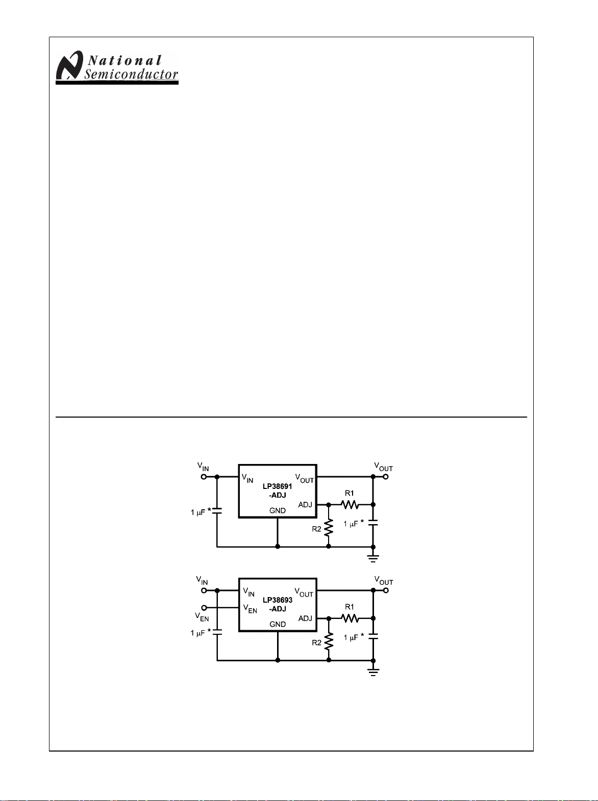
Typical Application Circuits
Features
Output voltage range of 1.25V - 9V
■
2.0% adjust pin voltage accuracy (25°C)
■
Low dropout voltage: 250mV @ 500mA (typ, 5V out)
■
Wide input voltage range (2.7V to 10V)
■
Precision (trimmed) bandgap reference
■
Guaranteed specs for -40°C to +125°C
■
1µA off-state quiescent current
■
Thermal overload protection
■
Foldback current limiting
■
SOT-223 and 6-Lead LLP packages
■
Enable pin (LP38693-ADJ)
■
Applications
Hard Disk Drives
■
Notebook Computers
■
Battery Powered Devices
■
Portable Instrumentation
■
20126801
20126802
V
= V
OUT
Note:
*Minimum value required for stability.
© 2008 National Semiconductor Corporation 201268 www.national.com
x (1 + R1/R2)
ADJ
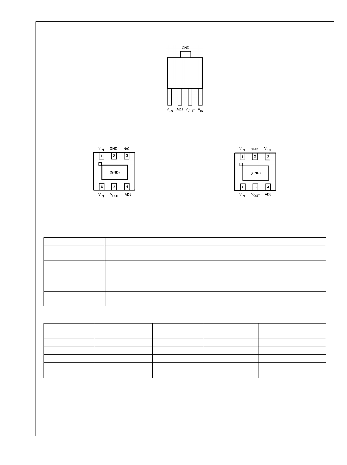
Connection Diagrams
LP38691-ADJ/LP38693-ADJ
6-Lead LLP, Bottom View
LP38691SD-ADJ
Pin Descriptions
Pin Description
V
IN
GND Circuit ground for the regulator. This is connected to the die through the lead frame, and also functions
V
OUT
V
EN
ADJ The adjust pin is used to set the regulated output voltage by connecting it to the external resistors
SOT-223, Top View
20126803
LP38693MP-ADJ
20126804
6-Lead LLP, Bottom View
20126805
LP38693SD-ADJ
This is the input supply voltage to the regulator. For LLP package devices, both VIN pins must be tied
together for full current operation (250mA maximum per pin).
as the heat sink when the large ground pad is soldered down to a copper plane.
Regulated output voltage.
The enable pin allows the part to be turned ON and OFF by pulling this pin high or low.
R1 and R2 (see Typical Application Circuit).
Ordering Information
Order Number Package Marking Package Type Package Drawing Supplied As
LP38691SD-ADJ L117B 6-Lead LLP SDE06A 1000 Units Tape and Reel
LP38693SD-ADJ L127B 6-Lead LLP SDE06A 1000 Units Tape and Reel
LP38693MP-ADJ LJUB SOT-223 MP05A 1000 Units Tape and Reel
LP38691SDX-ADJ L117B 6-Lead LLP SDE06A 4500 Units Tape and Reel
LP38693SDX-ADJ L127B 6-Lead LLP SDE06A 4500 Units Tape and Reel
LP38693MPX-ADJ LJUB SOT-223 MP05A 2000 Units Tape and Reel
www.national.com 2
LP38691-ADJ/LP38693-ADJ
Absolute Maximum Ratings (Note 1)
If Military/Aerospace specified devices are required,
please contact the National Semiconductor Sales Office/
V(max) All pins (with respect to GND) -0.3V to 12V
I
OUT
Junction Temperature −40°C to +150°C
Distributors for availability and specifications.
Storage Temperature Range −65°C to +150°C
Lead Temp. (Soldering, 5 seconds) 260°C
ESD Rating (Note 3) 2 kV
Power Dissipation (Note 2) Internally Limited
Electrical Characteristics Limits in standard typeface are for T
the full operating temperature range. Unless otherwise specified: VIN = V
Operating Ratings
VIN Supply Voltage 2.7V to 10V
Operating Junction
Temperature Range
= 25°C, and limits in boldface type apply over
J
+ 1V, CIN = C
OUT
limits are guaranteed through testing, statistical correlation, or design.
Symbol Parameter Conditions Min
VIN = 2.7V
V
ADJ
ADJ Pin Voltage
3.2V ≤ VIN ≤ 10V
100 µA < IL < 0.5A
ΔVO/ΔV
ΔVO/ΔI
L
Output Voltage Line Regulation
IN
(Note 6)
Output Voltage Load Regulation
(Note 7)
VO + 0.5V ≤ VIN ≤ 10V
IL = 25mA
1 mA < IL < 0.5A
VIN = VO + 1V
(VO = 2.5V)
IL = 0.1A
IL = 0.5A
(VO = 3.3V)
VIN - V
O
Dropout Voltage (Note 8)
IL = 0.1A
IL = 0.5A
(VO = 5V)
IL = 0.1A
IL = 0.5A
I
Q
Quiescent Current
VIN ≤ 10V, IL = 100 µA - 0.5A
VEN ≤ 0.4V,
(LP38693-ADJ Only)
IL(MIN) Minimum Load Current
I
FB
Foldback Current Limit VIN - VO > 5V
VIN - VO ≤ 4V
VIN - VO < 4V 850
PSRR Ripple Rejection VIN = VO + 2V(DC), with 1V(p-p) /
120Hz Ripple
T
SD
Thermal Shutdown Activation
(Junction Temp)
TSD (HYST) Thermal Shutdown Hysteresis
(Junction Temp)
I
ADJ
ADJ Input Leakage Current V
= 0 - 1.5V
ADJ
VIN = 10V
Internally Limited
−40°C to +125°C
= 10 µF, I
OUT
Typ (Note 4)
= 10mA. Min/Max
LOAD
Max Units
1.225 1.25 1.275
1.200 1.25 1.300
0.03 0.1 %/V
1.8 5 %/A
80
430
65
330
45
250
145
725
110
550
100
450
55 100
0.001 1
100
350
55 dB
160
10
-100 0.01 100 nA
V
mV
µA
mA
°C
3 www.national.com
Symbol Parameter Conditions Min
e
n
Output Noise BW = 10Hz to 10kHz
VO = 3.3V
VO (LEAK) Output Leakage Current VO = VO(NOM) + 1V @ VIN = 10V
V
EN
Enable Voltage (LP38693-ADJ
Only)
Output = OFF 0.4
Output = ON, VIN = 4V 1.8
Typ (Note 4)
0.7
0.5 2 µA
Max Units
Output = ON, VIN = 6V 3.0
Output = ON, VIN = 10V 4.0
I
EN
LP38691-ADJ/LP38693-ADJ
Note 1: Absolute maximum ratings indicate limits beyond which damage to the component may occur. Operating ratings indicate conditions for which the device
is intended to be functional, but do not guarantee specific performance limits. For guaranteed specifications, see Electrical Characteristics. Specifications do not
apply when operating the device outside of its rated operating conditions.
Note 2: At elevated temperatures, device power dissipation must be derated based on package thermal resistance and heatsink values (if a heatsink is used).
The junction-to-ambient thermal resistance (θ
copper area (less than 0.1 square inch). If one square inch of copper is used as a heat dissipator for the SOT-223, the θ
θ
values for the LLP package are also dependent on trace area, copper thickness, and the number of thermal vias used (refer to application note AN-1187). If
J-A
power disspation causes the junction temperature to exceed specified limits, the device will go into thermal shutdown.
Note 3: ESD is tested using the human body model which is a 100pF capacitor discharged through a 1.5k resistor into each pin.
Note 4: Typical numbers represent the most likely parametric norm for 25°C operation.
Note 5: If used in a dual-supply system where the regulator load is returned to a negative supply, the output pin must be diode clamped to ground.
Note 6: Output voltage line regulation is defined as the change in output voltage from nominal value resulting from a change in input voltage.
Note 7: Output voltage load regulation is defined as the change in output voltage from nominal value as the load current increases from 1mA to full load.
Note 8: Dropout voltage is defined as the minimum input to output differential required to maintain the output within 100mV of nominal value.
Enable Pin Leakage (LP38693ADJ Only)
) for the SOT-223 is approximately 125 °C/W for a PC board mounting with the device soldered down to minimum
J-A
VEN = 0V or 10V, VIN = 10V -1 0.001 1
drops to approximately 70 °C/W. The
J-A
µV/
V
µA
www.national.com 4
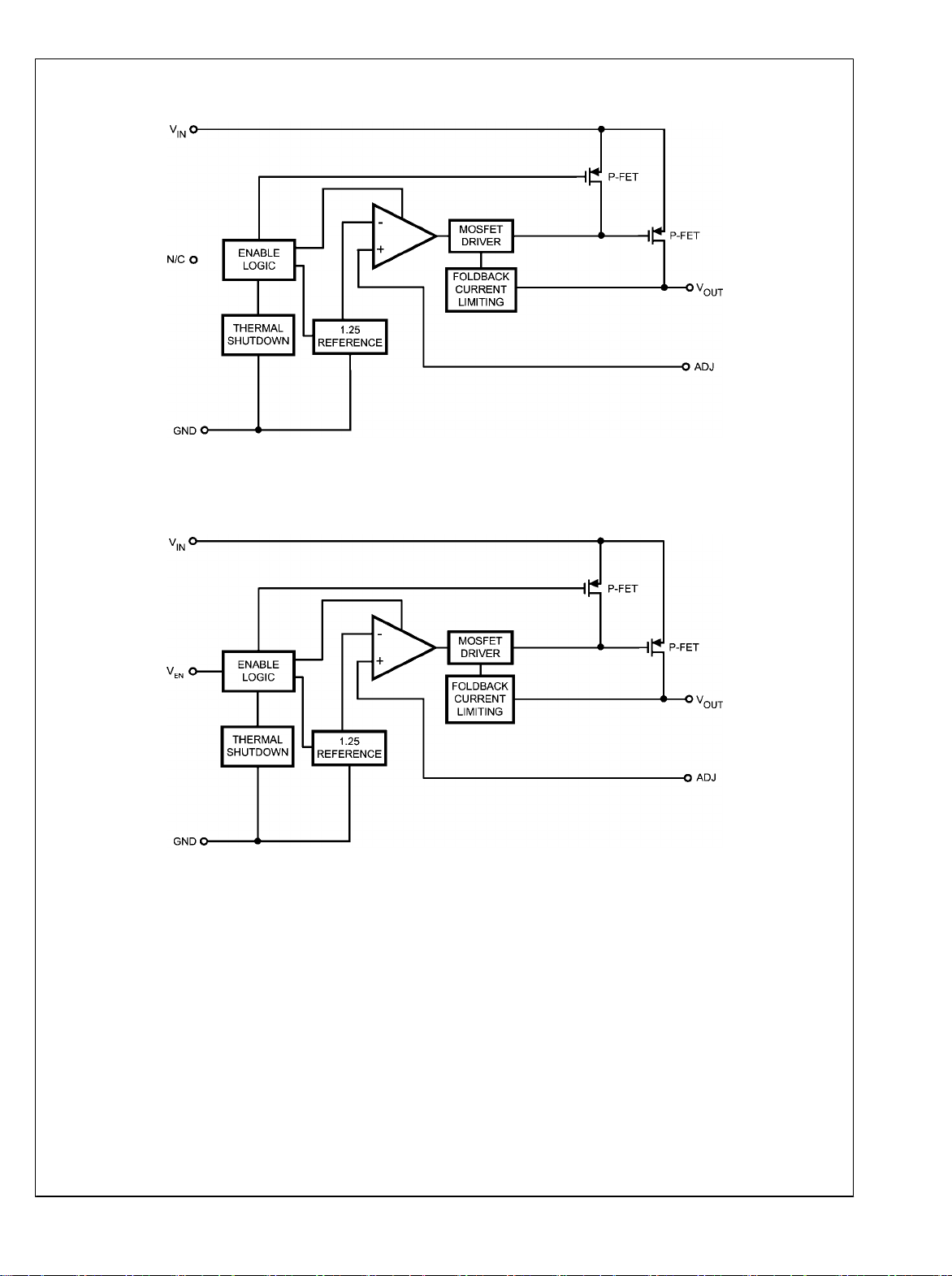
Block Diagrams
LP38691-ADJ/LP38693-ADJ
20126806
FIGURE 1. LP38691-ADJ Functional Diagram (LLP)
FIGURE 2. LP38693-ADJ Functional Diagram (SOT-223, LLP)
5 www.national.com
20126807
 Loading...