

查询LP3852EMPX-1.8供应商
LP3852/LP3855
1.5A Fast Response Ultra Low Dropout Linear
Regulators
LP3852/LP3855 1.5A Fast Response Ultra Low Dropout Linear Regulators
March 2004
General Description
The LP3852/LP3855 series of fast ultra low-dropout linear
regulators operate from a +2.5V to +7.0V input supply. Wide
range of preset output voltage options are available. These
ultra low dropout linear regulators respond very quickly to
step changes in load, which makes them suitable for low
voltage microprocessor applications. The LP3852/LP3855
are developed on a CMOS process which allows low quiescent current operation independent of output load current.
This CMOS process also allows the LP3852/LP3855 to operate under extremely low dropout conditions.
Dropout Voltage: Ultra low dropout voltage; typically 24mV
at 150mA load current and 240mV at 1.5A load current.
Ground Pin Current: Typically 4mA at 1.5A load current.
Shutdown Mode: Typically 10nA quiescent current when
the shutdown pin is pulled low.
Error Flag: Error flag goes low when the output voltage
drops 10% below nominal value.
SENSE: Sense pin improves regulation at remote loads.
Precision Output Voltage: Multiple output voltage options
are available ranging from 1.8V to 5.0V with a guaranteed
accuracy of
conditions (varying line, load, and temperature).
±
1.5% at room temperature, and±3.0% over all
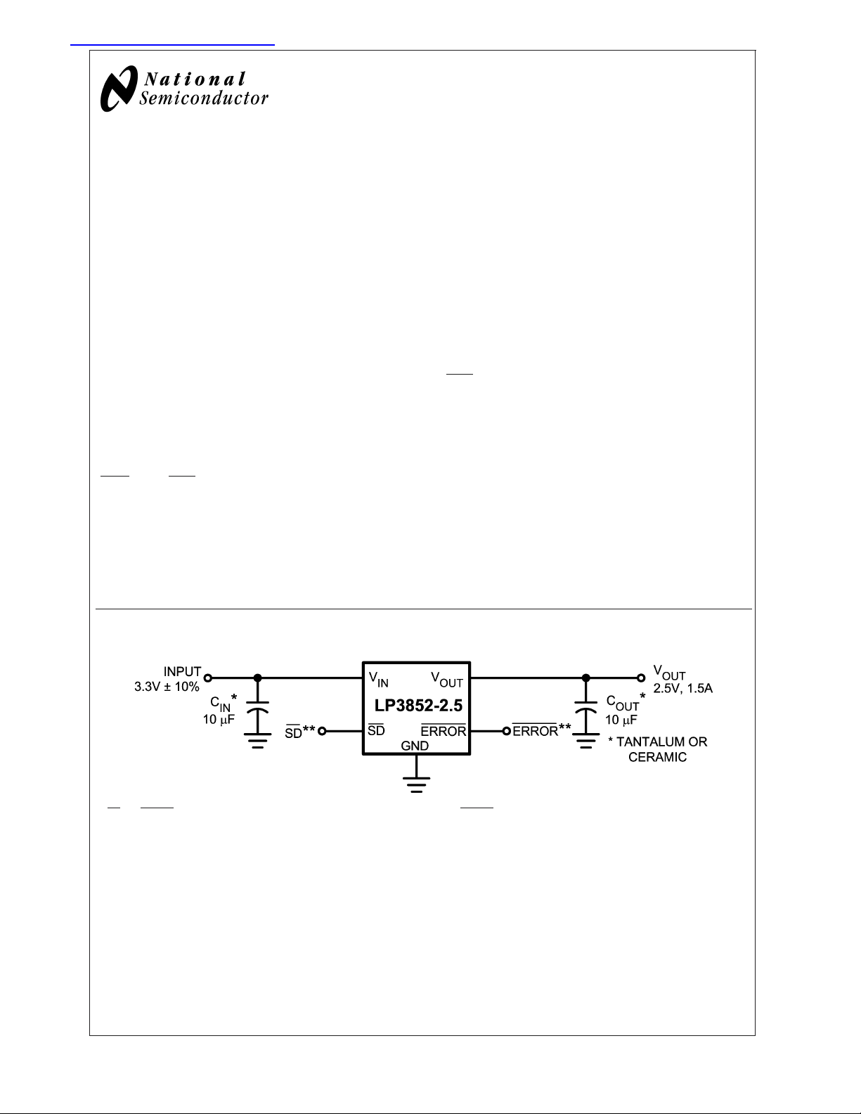
Typical Application Circuits
Features
n Ultra low dropout voltage
n Stable with selected ceramic capacitors
n Low ground pin current
n Load regulation of 0.06%
n 10nA quiescent current in shutdown mode
n Guaranteed output current of 1.5A DC
n Available in TO-263, TO-220 and SOT-223 packages
n Output voltage accuracy
n Error flag indicates output status
n Sense option improves load regulation
n Overtemperature/overcurrent protection
n −40˚C to +125˚C junction temperature range
±
1.5%
Applications
n Microprocessor power supplies
n GTL, GTL+, BTL, and SSTL bus terminators
n Power supplies for DSPs
n SCSI terminator
n Post regulators
n High efficiency linear regulators
n Battery chargers
n Other battery powered applications
**SD and ERROR pins must be pulled high through a 10kΩ pull-up resistor. Connect the ERROR pin to ground if this function is not used. See Application Hints
for more information.
© 2004 National Semiconductor Corporation DS200310 www.national.com
20031001
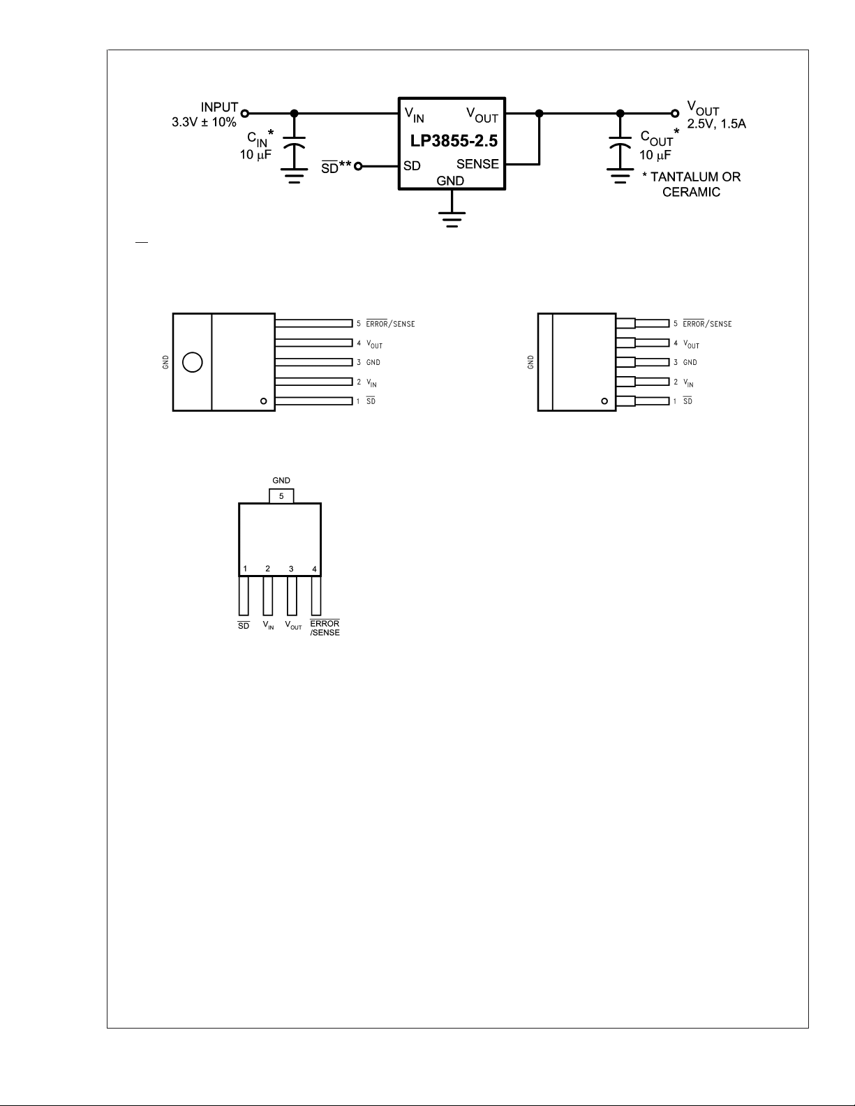
Typical Application Circuits (Continued)
LP3852/LP3855
**SD must be pulled high through a 10kΩ pull-up resistor. See Application Hints for more information.
Connection Diagrams
20031005
Top View
TO220-5 Package
Bent, Staggered Leads
20031034
20031006
Top View
TO263-5 Package
Top View
20031096
SOT223-5 Package
www.national.com 2
Pin Description for TO220-5 and TO263-5 Packages
#
Pin
Name Function Name Function
1SD
2V
IN
3 GND Ground GND Ground
4V
OUT
5 ERROR
LP3852 LP3855
Shutdown SD Shutdown
Input Supply V
Output Voltage V
IN
OUT
ERROR Flag SENSE Remote Sense Pin
Pin Description for SOT223-5 Package
#
Pin
Name Function Name Function
1SD
2V
3V
IN
OUT
4 ERROR
5 GND Ground GND Ground
LP3852 LP3855
Shutdown SD Shutdown
Input Supply V
Output Voltage V
IN
OUT
ERROR Flag SENSE Remote Sense Pin
LP3852/LP3855
Input Supply
Output Voltage
Input Supply
Output Voltage
www.national.com3
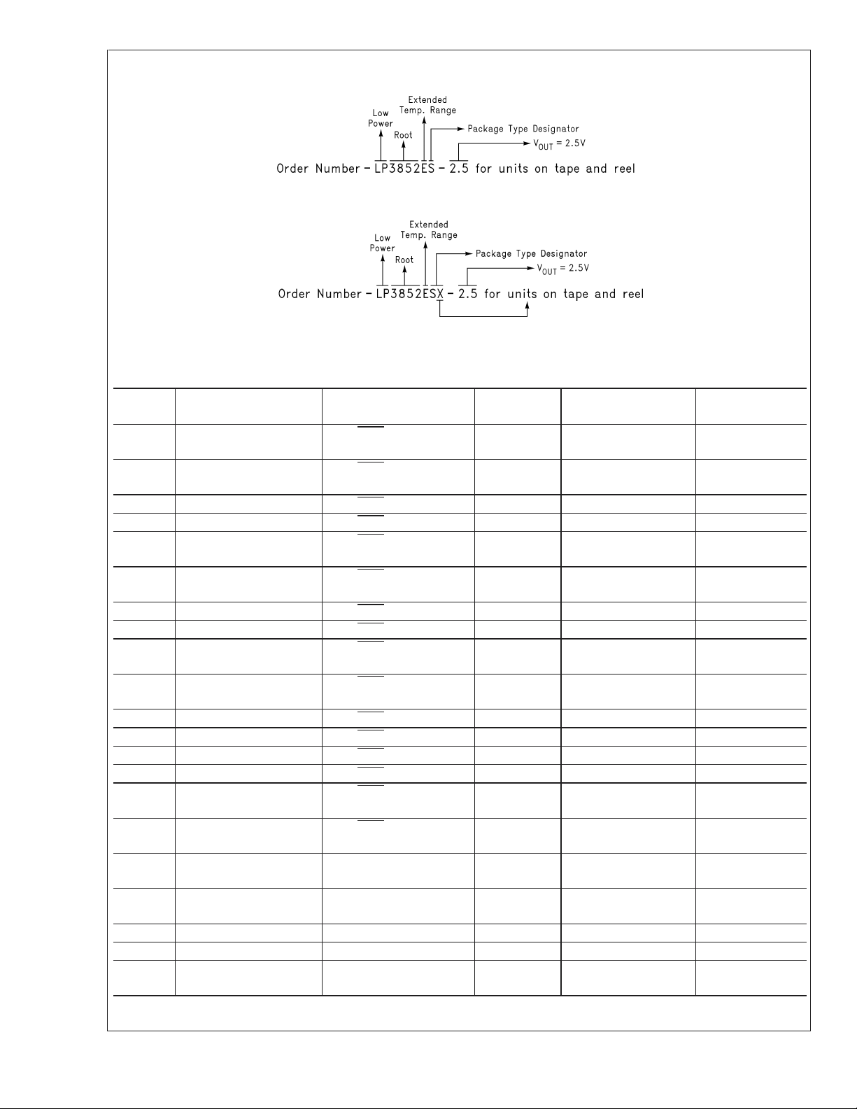
Ordering Information
LP3852/LP3855
Package Type Designator is "T" for TO220 package, and "S" for TO263 package.
TABLE 1. Package Marking and Ordering Information
Output
Voltage Order Number
5.0 LP3852EMP-5.0 1.5A, Error Flag
5.0 LP3852EMPX-5.0 1.5A, Error Flag SOT223-5 LHXB 2000 Units on
5.0 LP3852ES-5.0 1.5A, Error Flag
5.0 LP3852ESX-5.0 1.5A, Error Flag
3.3 LP3852EMP-3.3 1.5A, Error Flag
3.3 LP3852EMPX-3.3 1.5A, Error Flag SOT223-5 LHVB 2000 Units on
3.3 LP3852ES-3.3 1.5A, Error Flag
3.3 LP3852ESX-3.3 1.5A, Error Flag
2.5 LP3852EMP-2.5 1.5A, Error Flag
2.5 LP3852EMPX-2.5 1.5A, Error Flag SOT223-5 LHUB 2000 Units on
2.5 LP3852ES-2.5 1.5A, Error Flag
2.5 LP3852ESX-2.5 1.5A, Error Flag
1.8 LP3852ES-1.8 1.5A, Error Flag
1.8 LP3852ESX-1.8 1.5A, Error Flag
1.8 LP3852EMP-1.8 1.5A, Error Flag
1.8 LP3852EMPX-1.8 1.5A, Error Flag
5.0 LP3855EMP-5.0 1.5A, SENSE SOT223-5 LJ2B 1000 Units on
5.0 LP3855EMPX-5.0 1.5A, SENSE SOT223-5 LJ2B 2000 Units on
5.0 LP3855ES-5.0 1.5A, SENSE TO263-5 LP3855ES-5.0 Rail
5.0 LP3855ESX-5.0 1.5A, SENSE TO263-5 LP3855ES-5.0 Tape and Reel
3.3 LP3855EMP-3.3 1.5A, SENSE SOT223-5 LJ1B 1000 Units on
Description
(Current, Option)
Package
Type Package Marking Supplied As:
SOT223-5 LHXB 1000 Units on
TO263-5 LP3852ES-5.0 Rail
TO263-5 LP3852ES-5.0 Tape and Reel
SOT223-5 LHVB 1000 Units on
TO263-5 LP3852ES-3.3 Rail
TO263-5 LP3852ES-3.3 Tape and Reel
SOT223-5 LHUB 1000 Units on
TO263-5 LP3852ES-2.5 Rail
TO263-5 LP3852ES-2.5 Tape and Reel
TO263-5 LP3852ES-1.8 Rail
TO263-5 LP3852ES-1.8 Tape and Reel
SOT223-5 LHTB 1000 Units on
SOT223-5 LHTB 2000 Units on
20031031
Tape and Reel
Tape and Reel
Tape and Reel
Tape and Reel
Tape and Reel
Tape and Reel
Tape and Reel
Tape and Reel
Tape and Reel
Tape and Reel
Tape and Reel
www.national.com 4
Ordering Information (Continued)
TABLE 1. Package Marking and Ordering Information (Continued)
Output
Voltage Order Number
3.3 LP3855EMPX-3.3 1.5A, SENSE SOT223-5 LJ1B 2000 Units on
3.3 LP3855ES-3.3 1.5A, SENSE TO263-5 LP3855ES-3.3 Rail
3.3 LP3855ESX-3.3 1.5A, SENSE TO263-5 LP3855ES-3.3 Tape and Reel
2.5 LP3855EMP-2.5 1.5A, SENSE SOT223-5 LHZB 1000 Units on
2.5 LP3855EMPX-2.5 1.5A, SENSE SOT223-5 LHZB 2000 Units on
2.5 LP3855ES-2.5 1.5A, SENSE TO263-5 LP3855ES-2.5 Rail
2.5 LP3855ESX-2.5 1.5A, SENSE TO263-5 LP3855ES-2.5 Tape and Reel
1.8 LP3855EMP-1.8 1.5A, SENSE SOT223-5 LHYB 1000 Units on
1.8 LP3855EMPX-1.8 1.5A, SENSE SOT223-5 LHYB
1.8 LP3855ES-1.8 1.5A, SENSE TO263-5 LP3855ES-1.8 Rail
1.8 LP3855ESX-1.8 1.5A, SENSE TO263-5 LP3855ES-1.8 Tape and Reel
5.0 LP3852ET-5.0 1.5A, Error Flag
3.3 LP3852ET-3.3 1.5A, Error Flag
2.5 LP3852ET-2.5 1.5A, Error Flag
1.8 LP3852ET-1.8 1.5A, Error Flag
5.0 LP3855ET-5.0 1.5A, SENSE TO220-5 LP3855ET-5.0 Rail
3.3 LP3855ET-3.3 1.5A, SENSE TO220-5 LP3855ET-3.3 Rail
2.5 LP3855ET-2.5 1.5A, SENSE TO220-5 LP3855ET-2.5 Rail
1.8 LP3855ET-1.8 1.5A, SENSE TO220-5 LP3855ET-1.8 Rail
Description
(Current, Option)
Package
Type Package Marking Supplied As:
Tape and Ree
Tape and Reel
Tape and Ree
Tape and Reel
TO220-5 LP3852ET-5.0 Rail
TO220-5 LP3852ET-3.3 Rail
TO220-5 LP3852ET-2.5 Rail
TO220-5 LP3852ET-1.8 Rail
LP3852/LP3855
www.national.com5
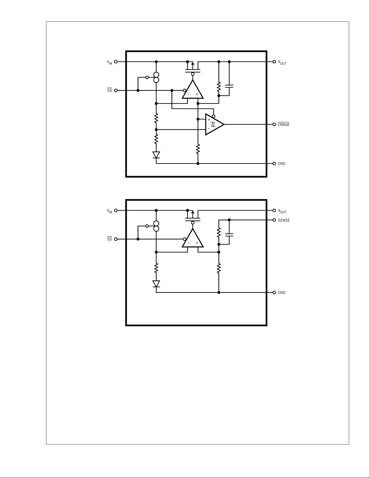
Block Diagrams
LP3852/LP3855
LP3852
20031003
LP3855
www.national.com 6
20031029

LP3852/LP3855
Absolute Maximum Ratings (Note 1)
If Military/Aerospace specified devices are required,
please contact the National Semiconductor Sales Office/
Distributors for availability and specifications.
I
(Survival) Short Circuit Protected
OUT
Maximum Voltage for ERROR
Pin V
Maximum Voltage for SENSE Pin V
Storage Temperature Range −65˚C to +150˚C
Lead Temperature
Operating Ratings
(Soldering, 5 sec.) 260˚C
ESD Rating (Note 3) 2 kV
Power Dissipation (Note 2) Internally Limited
Input Supply Voltage (Survival) −0.3V to +7.5V
Shutdown Input Voltage
Input Supply Voltage (Note 11) 2.5V to 7.0V
Shutdown Input Voltage −0.3V to 7.0V
Maximum Operating Current (DC) 1.5A
Junction Temperature −40˚C to +125˚C
(Survival) −0.3V to 7.5V
Output Voltage (Survival), (Note
6), (Note 7) −0.3V to +6.0V
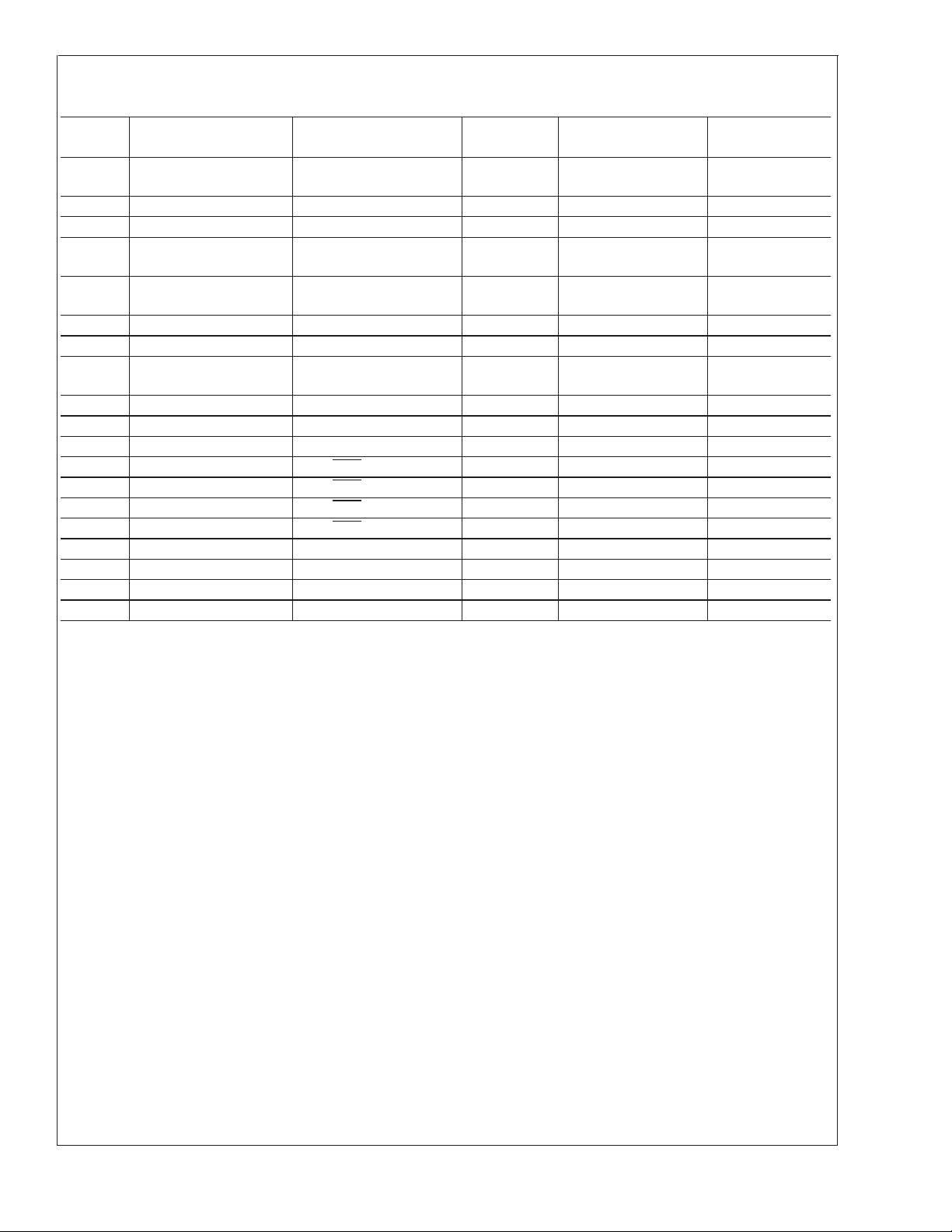
Electrical Characteristics
LP3852/LP3855
Limits in standard typeface are for TJ= 25˚C, and limits in boldface type apply over the full operating temperature range.
Unless otherwise specified: V
IN=VO(NOM)
+ 1V, IL= 10 mA, C
Symbol Parameter Conditions Typ
Output Voltage
V
O
Tolerance
+1V ≤ VIN≤ 7.0V
V
OUT
10 mA ≤ I
≤ 1.5A 0
L
(Note 8)
∆V
OL
Output Voltage Line
V
+1V ≤ VIN≤ 7.0V 0.02
OUT
Regulation (Note 8)
∆V
/ ∆I
O
OUT
Output Voltage Load
10 mA ≤ I
≤ 1.5A 0.06
L
Regulation
(Note 8)
= 150 mA 24 35
V
IN-VOUT
I
GND
I
GND
I
O(PK)
Dropout Voltage
TO-263 and TO-220
(Note 10)
Dropout Voltage
SOT 223
(Note 10), (Note 12)
Ground Pin Current In
Normal Operation Mode
Ground Pin Current In
Shutdown Mode
Peak Output Current VO≥ V
I
L
IL= 1.5A 240 280
= 150mA 26 35
I
L
= 1.5A 260 320
I
L
I
= 150 mA 3 9
L
IL= 1.5A 3 9
VSD≤ 0.3V 0.01 10 µA
-40˚C ≤ T
≤ 85˚C 50
J
- 4% 1.8 A
O(NOM)
Short Circuit Protection
I
SC
Short Circuit Current 3.2 A
= 10µF, VSD= 2V.
OUT
(Note
4)
0.06
0.12
LP3852/5 (Note 5) Units
Min Max
-1.5
-3.0
+1.5
+3.0
45
380
45
435
10
10
IN
OUT
%
%
%
mV
mA
www.national.com7

Electrical Characteristics
LP3852/LP3855
Limits in standard typeface are for TJ= 25˚C, and limits in boldface type apply over the full operating temperature range.
Unless otherwise specified: V
LP3852/LP3855
Symbol Parameter Conditions Typ
Shutdown Input
V
SDT
T
dOFF
T
dON
I
SD
Error Flag
V
T
V
TH
V
EF(Sat)
Td Flag Reset Delay 1 µs
I
lk
I
max
AC Parameters
PSRR Ripple Rejection
ρ
n(l/f)
e
n
Note 1: Absolute maximum ratings indicate limits beyond which damage to the device may occur. Operating ratings indicate conditions for which the device is
intended to be functional, but does not guarantee specific performance limits. For guaranteed specifications and test conditions, see Electrical Characteristics. The
guaranteed specifications apply only for the test conditions listed. Some performance characteristics may degrade when the device is not operated under the listed
test conditions.
Note 2: At elevated temperatures, devices must be derated based on package thermal resistance. The devices in TO220 package must be derated at θ
(with 0.5in
0.5in
Note 3: The human body model is a 100pF capacitor discharged through a 1.5kΩ resistor into each pin.
Note 4: Typical numbers are at 25˚C and represent the most likely parametric norm.
Note 5: Limits are guaranteed by testing, design, or statistical correlation.
Note 6: If used in a dual-supply system where the regulator load is returned to a negative supply, the output must be diode-clamped to ground.
Note 7: The output PMOS structure contains a diode between the V
if the voltage at the output terminal is forced to be higher than the voltage at the input terminal. This diode can typically withstand 200mA of DC current and 1Amp
of peak current.
Note 8: Output voltage line regulation is defined as the change in output voltage from the nominal value due to change in the input line voltage. Output voltage load
regulation is defined as the change in output voltage from the nominal value due to change in load current. The line and load regulation specification contains only
the typical number. However, the limits for line and load regulation are included in the output voltage tolerance specification.
Note 9: Error Flag threshold and hysteresis are specified as percentage of regulated output voltage. See Application Hints.
Note 10: Dropout voltage is defined as the minimum input to output differential voltage at which the output drops 2% below the nominal value. Dropout voltage
specification applies only to output voltages of 2.5V and above. For output voltages below 2.5V, the drop-out voltage is nothing but the input to output differential,
since the minimum input voltage is 2.5V.
Note 11: The minimum operating value for V
Note 12: The SOT 223 package devices have slightly higher dropout due to increased bond wire resistance.
2
2
, 1oz. copper area), junction-to-ambient. See Application Hints.
Shutdown Threshold
Turn-off delay IL= 1.5A 20 µs
Turn-on delay IL= 1.5A 25 µs
SD Input Current VSD=V
Threshold (Note 9) 10 516 %
Threshold Hysteresis (Note 9) 5 28 %
Error Flag Saturation I
Error Flag Pin Leakage
Current
Error Flag Pin Sink
Current
Output Noise Density f = 120Hz 0.8 µV
Output Noise Voltage
, 1oz. copper area), junction-to-ambient (with no heat sink). The devices in the TO263 surface-mount package must be derated at θjA= 60˚C/W (with
(Continued)
IN=VO(NOM)
IN
+ 1V, IL= 10 mA, C
Output = High V
Output = Low 0 0.3
= 100µA 0.02 0.1 V
sink
V
Error
V
IN=VOUT
C
OUT
V
OUT
V
IN=VOUT
C
OUT
V
OUT
BW = 10Hz – 100kHz
V
OUT
BW = 300Hz – 300kHz
V
OUT
is equal to either [V
= 10µF, VSD= 2V.
OUT
LP3852/5 (Note 5) Units
(Note
4)
IN
IN
1nA
Min Max
2
1nA
= 0.5V 1mA
+1V
73
= 10uF
= 3.3V, f = 120Hz
+ 0.5V
57
= 10uF
= 3.3V, f = 120Hz
150
= 2.5V
100
= 2.5V
and V
IN
OUT(NOM)+VDROPOUT
terminals. This diode is normally reverse biased. This diode will get forward biased
OUT
] or 2.5V, whichever is greater.
V
dB
µV (rms)
= 50˚C/W
jA
www.national.com 8

LP3852/LP3855
Typical Performance Characteristics Unless otherwise specified: T
= 10µF, S/D pin is tied to VIN,V
C
IN
Dropout Voltage vs Output Load Current
Shutdown IQvs Junction Temperature Errorflag Threshold vs Junction Temperature
= 2.5V, VIN=V
OUT
20031062
+ 1V, IL=10mA.
O(NOM)
Ground Current vs Output Voltage
= 25˚C, C
J
= 1.5A
I
L
OUT
= 10µF,
20031054
20031055
DC Load Reg. vs Junction Temperature DC Line Regulation vs Temperature
20031058 20031059
20031057
www.national.com9

Typical Performance Characteristics Unless otherwise specified: T
= 10µF, S/D pin is tied to VIN,V
C
IN
LP3852/LP3855
V
IN
vs V
Over Temperature Noise vs Frequency
OUT
= 2.5V, VIN=V
OUT
+ 1V, IL= 10 mA. (Continued)
O(NOM)
= 25˚C, C
J
OUT
= 10µF,
Load Transient Response
C
IN=COUT
= 10µF, OSCON
Load Transient Response
C
IN=COUT
= 100µF, POSCAP
20031060
20031081
Load Transient Response
CIN=C
= 100µF, OSCON
OUT
Load Transient Response
CIN=C
= 10µF, TANTALUM
OUT
20031061
20031082
20031083 20031084
www.national.com 10

LP3852/LP3855
Typical Performance Characteristics Unless otherwise specified: T
= 10µF, S/D pin is tied to VIN,V
C
IN
Load Transient Response
C
IN=COUT
= 100µF, TANTALUM
Load Transient Response
= 2 x 10µF CERAMIC
C
IN
= 2 x 10µF CERAMIC
C
OUT
= 2.5V, VIN=V
OUT
20031085
+ 1V, IL= 10 mA. (Continued)
O(NOM)
Load Transient Response
C
= 2 x 10µF CERAMIC
IN
= 2 x 10µF CERAMIC
C
OUT
= 25˚C, C
J
OUT
= 10µF,
20031093
20031094
www.national.com11

Application Hints
VINRESTRICTIONS FOR PROPER START-UP
To prevent misoperation, ensure that V
before start-up is initiated. This scenario can occur in systems with a backup battery using reverse-biased "blocking"
LP3852/LP3855
diodes which may allow enough leakage current to flow into
node to raise it’s voltage slightly above ground when
the V
IN
the main power is removed. Using low leakage diodes or a
resistive pull down can prevent the voltage at V
above 50mV. Large bulk capacitors connected to V
also cause a start-up problem if they do not discharge fully
before re-start is initiated (but only if V
below 1V). A resistor connected across the capacitor will
allow it to discharge more quickly. It should be noted that the
probability of a "false start" caused by incorrect logic states
is extremely low.
EXTERNAL CAPACITORS
Like any low-dropout regulator, external capacitors are required to assure stability. these capacitors must be correctly
selected for proper performance.
INPUT CAPACITOR: An input capacitor of at least 10µF is
required. Ceramic or Tantalum may be used, and capacitance may be increased without limit
OUTPUT CAPACITOR: An output capacitor is required for
loop stability. It must be located less than 1 cm from the
device and connected directly to the output and ground pins
using traces which have no other currents flowing through
them (see PCB Layout section).
The minimum amount of output capacitance that can be
used for stable operation is 10µF. For general usage across
all load currents and operating conditions, the part was
characterized using a 10µF Tantalum input capacitor. The
minimum and maximum stable ESR range for the output
capacitor was then measured which kept the device stable,
assuming any output capacitor whose value is greater than
10µF (see Figure 1 below).
is below 50mV
IN
is allowed to fall
IN
from rising
IN
IN
may
OPERATION WITH CERAMIC OUTPUT CAPACITORS
LP385X voltage regulators can operate with ceramic output
capacitors if the values of the input and output capacitors are
selected appropriately. The total ceramic output capacitance
must be equal to or less than a specified maximum value in
order for the regulator to remain stable over all operating
conditions. This maximum amount of ceramic output capacitance is dependent upon the amount of ceramic input capacitance used as well as the load current of the application.
This relationship is shown in Figure 2, which graphs the
maximum stable value of ceramic output capacitance as a
function of ceramic input capacitance for load currents of
1.5A.
20031095
FIGURE 2. Maximum Ceramic Output Capacitance vs
Ceramic Input Capacitance
If the maximum load current is 1.5A and a 10µF ceramic
input capacitor is used, the regulator will be stable with
ceramic output capacitor values from 10µF up to about
150µF. When calculating the total ceramic output capacitance present in an application, it is necessary to include any
ceramic bypass capacitors connected to the regulator output.
20031070
FIGURE 1. ESR Curve for C
(with 10µF Tantalum
OUT
Input Capacitor)
It should be noted that it is possible to operate the part with
an output capacitor whose ESR is below these limits, assuming that sufficient ceramic input capacitance is provided.
This will allow stable operation using ceramic output capacitors (see next section).
www.national.com 12
SELECTING A CAPACITOR
It is important to note that capacitance tolerance and variation with temperature must be taken into consideration when
selecting a capacitor so that the minimum required amount
of capacitance is provided over the full operating temperature range. In general, a good Tantalum capacitor will show
very little capacitance variation with temperature, but a ceramic may not be as good (depending on dielectric type).
Aluminum electrolytics also typically have large temperature
variation of capacitance value.
Equally important to consider is a capacitor’s ESR change
with temperature: this is not an issue with ceramics, as their
ESR is extremely low. However, it is very important in Tantalum and aluminum electrolytic capacitors. Both show increasing ESR at colder temperatures, but the increase in
aluminum electrolytic capacitors is so severe they may not
be feasible for some applications (see Capacitor Characteristics Section).

Application Hints (Continued)
CAPACITOR CHARACTERISTICS
CERAMIC: For values of capacitance in the 10 to 100 µF
range, ceramics are usually larger and more costly than
tantalums but give superior AC performance for bypassing
high frequency noise because of very low ESR (typically less
than 10 mΩ). However, some dielectric types do not have
good capacitance characteristics as a function of voltage
and temperature.
Z5U and Y5V dielectric ceramics have capacitance that
drops severely with applied voltage. A typical Z5U or Y5V
capacitor can lose 60% of its rated capacitance with half of
the rated voltage applied to it. The Z5U and Y5V also exhibit
a severe temperature effect, losing more than 50% of nominal capacitance at high and low limits of the temperature
range.
X7R and X5R dielectric ceramic capacitors are strongly recommended if ceramics are used, as they typically maintain a
capacitance range within
ing ratings of temperature and voltage. Of course, they are
typically larger and more costly than Z5U/Y5U types for a
given voltage and capacitance.
TANTALUM: Solid Tantalum capacitors are typically recommended for use on the output because their ESR is very
close to the ideal value required for loop compensation.
Tantalums also have good temperature stability: a good
quality Tantalum will typically show a capacitance value that
varies less than 10-15% across the full temperature range of
125˚C to −40˚C. ESR will vary only about 2X going from the
high to low temperature limits.
The increasing ESR at lower temperatures can cause oscillations when marginal quality capacitors are used (if the ESR
of the capacitor is near the upper limit of the stability range at
room temperature).
ALUMINUM: This capacitor type offers the most capacitance for the money. The disadvantages are that they are
larger in physical size, not widely available in surface mount,
and have poor AC performance (especially at higher frequencies) due to higher ESR and ESL.
Compared by size, the ESR of an aluminum electrolytic is
higher than either Tantalum or ceramic, and it also varies
greatly with temperature. A typical aluminum electrolytic can
exhibit an ESR increase of as much as 50X when going from
25˚C down to −40˚C.
It should also be noted that many aluminum electrolytics only
specify impedance at a frequency of 120 Hz, which indicates
they have poor high frequency performance. Only aluminum
electrolytics that have an impedance specified at a higher
frequency (between 20 kHz and 100 kHz) should be used for
the LP385X. Derating must be applied to the manufacturer’s
ESR specification, since it is typically only valid at room
temperature.
Any applications using aluminum electrolytics should be
thoroughly tested at the lowest ambient operating temperature where ESR is maximum.
PCB LAYOUT
Good PC layout practices must be used or instability can be
induced because of ground loops and voltage drops. The
input and output capacitors must be directly connected to the
input, output, and ground pins of the regulator using traces
which do not have other currents flowing in them (Kelvin
connect).
±
20% of nominal over full operat-
The best way to do this is to lay out C
device with short traces to the V
IN,VOUT
and C
IN
, and ground pins.
OUT
near the
The regulator ground pin should be connected to the external circuit ground so that the regulator and its capacitors
have a "single point ground".
It should be noted that stability problems have been seen in
applications where "vias" to an internal ground plane were
used at the ground points of the IC and the input and output
capacitors. This was caused by varying ground potentials at
these nodes resulting from current flowing through the
ground plane. Using a single point ground technique for the
regulator and it’s capacitors fixed the problem.
Since high current flows through the traces going into V
and coming from V
, Kelvin connect the capacitor leads to
OUT
these pins so there is no voltage drop in series with the input
and output capacitors.
RFI/EMI SUSCEPTIBILITY
RFI (radio frequency interference) and EMI (electromagnetic
interference) can degrade any integrated circuit’s performance because of the small dimensions of the geometries
inside the device. In applications where circuit sources are
present which generate signals with significant high fre-
>
quency energy content (
1 MHz), care must be taken to
ensure that this does not affect the IC regulator.
If RFI/EMI noise is present on the input side of the regulator
(such as applications where the input source comes from the
output of a switching regulator), good ceramic bypass capacitors must be used at the input pin of the IC.
If a load is connected to the IC output which switches at high
speed (such as a clock), the high-frequency current pulses
required by the load must be supplied by the capacitors on
the IC output. Since the bandwidth of the regulator loop is
less than 100 kHz, the control circuitry cannot respond to
load changes above that frequency. This means the effective
output impedance of the IC at frequencies above 100 kHz is
determined only by the output capacitor(s).
In applications where the load is switching at high speed, the
output of the IC may need RF isolation from the load. It is
recommended that some inductance be placed between the
output capacitor and the load, and good RF bypass capacitors be placed directly across the load.
PCB layout is also critical in high noise environments, since
RFI/EMI is easily radiated directly into PC traces. Noisy
circuitry should be isolated from "clean" circuits where possible, and grounded through a separate path. At MHz frequencies, ground planes begin to look inductive and RFI/
EMI can cause ground bounce across the ground plane.
In multi-layer PCB applications, care should be taken in
layout so that noisy power and ground planes do not radiate
directly into adjacent layers which carry analog power and
ground.
OUTPUT NOISE
Noise is specified in two waysSpot Noise or Output noise density is the RMS sum of all
noise sources, measured at the regulator output, at a specific frequency (measured with a 1Hz bandwidth). This type
of noise is usually plotted on a curve as a function of frequency.
Total output Noise or Broad-band noise is the RMS sum
of spot noise over a specified bandwidth, usually several
decades of frequencies.
LP3852/LP3855
IN
www.national.com13

Application Hints (Continued)
Attention should be paid to the units of measurement. Spot
noise is measured in units µV/
noise is measured in µV(rms).
The primary source of noise in low-dropout regulators is the
LP3852/LP3855
internal reference. In CMOS regulators, noise has a low
frequency component and a high frequency component,
which depend strongly on the silicon area and quiescent
current. Noise can be reduced in two ways: by increasing the
transistor area or by increasing the current drawn by the
internal reference. Increasing the area will decrease the
chance of fitting the die into a smaller package. Increasing
the current drawn by the internal reference increases the
total supply current (ground pin current). Using an optimized
trade-off of ground pin current and die size, LP3852/LP3855
achieves low noise performance and low quiescent current
operation.
The total output noise specification for LP3852/LP3855 is
presented in the Electrical Characteristics table. The Output
noise density at different frequencies is represented by a
curve under typical performance characteristics.
SHORT-CIRCUIT PROTECTION
The LP3852 and LP3855 are short circuit protected and in
the event of a peak over-current condition, the short-circuit
control loop will rapidly drive the output PMOS pass element
√
Hz or nV/√Hz and total output
off. Once the power pass element shuts down, the control
loop will rapidly cycle the output on and off until the average
power dissipation causes the thermal shutdown circuit to
respond to servo the on/off cycling to a lower frequency.
Please refer to the section on thermal information for power
dissipation calculations.
ERROR FLAG OPERATION
The LP3852/LP3855 produces a logic low signal at the Error
Flag pin when the output drops out of regulation due to low
input voltage, current limiting, or thermal limiting. This flag
has a built in hysteresis. The timing diagram in Figure 3
shows the relationship between the ERROR flag and the
output voltage. In this example, the input voltage is changed
to demonstrate the functionality of the Error Flag.
The internal Error flag comparator has an open drain output
stage. Hence, the ERROR pin should be pulled high through
a pull up resistor. Although the ERROR flag pin can sink
current of 1mA, this current is energy drain from the input
supply. Hence, the value of the pull up resistor should be in
the range of 10kΩ to 1MΩ. The ERROR pin must be
connected to ground if this function is not used. It should
also be noted that when the shutdown pin is pulled low, the
ERROR pin is forced to be invalid for reasons of saving
power in shutdown mode.
FIGURE 3. Error Flag Operation
SENSE PIN
In applications where the regulator output is not very close to
the load, LP3855 can provide better remote load regulation
using the SENSE pin. Figure 4 depicts the advantage of the
SENSE option. LP3852 regulates the voltage at the output
pin. Hence, the voltage at the remote load will be the regulator output voltage minus the drop across the trace resis-
www.national.com 14
20031007
tance. For example, in the case of a 3.3V output, if the trace
resistance is 100mΩ, the voltage at the remote load will be
3.15V with 1.5A of load current, I
. The LP3855 regulates
LOAD
the voltage at the sense pin. Connecting the sense pin to the
remote load will provide regulation at the remote load, as
shown in Figure 4. If the sense option pin is not required, the
sense pin must be connected to the V
OUT
pin.

Application Hints (Continued)
FIGURE 4. Improving remote load regulation using LP3855
LP3852/LP3855
20031008
SHUTDOWN OPERATION
A CMOS Logic level signal at the shutdown ( SD) pin will
turn-off the regulator. Pin SD must be actively terminated
through a 10kΩ pull-up resistor for a proper operation. If this
pin is driven from a source that actively pulls high and low
(such as a CMOS rail to rail comparator), the pull-up resistor
is not required. This pin must be tied to Vin if not used.
DROPOUT VOLTAGE
The dropout voltage of a regulator is defined as the minimum
input-to-output differential required to stay within 2% of the
nominal output voltage. For CMOS LDOs, the dropout voltage is the product of the load current and the Rds(on) of the
internal MOSFET.
REVERSE CURRENT PATH
The internal MOSFET in LP3852 and LP3855 has an inherent parasitic diode. During normal operation, the input voltage is higher than the output voltage and the parasitic diode
is reverse biased. However, if the output is pulled above the
input in an application, then current flows from the output to
the input as the parasitic diode gets forward biased. The
output can be pulled above the input as long as the current
in the parasitic diode is limited to 200mA continuous and 1A
peak.
POWER DISSIPATION/HEATSINKING
LP3852 and LP3855 can deliver a continuous current of
1.5A over the full operating temperature range. A heatsink
may be required depending on the maximum power dissipation and maximum ambient temperature of the application.
Under all possible conditions, the junction temperature must
be within the range specified under operating conditions.
The total power dissipation of the device is given by:
=(VIN−V
P
D
where I
OUT)IOUT
is the operating ground current of the device
GND
+(VIN)I
GND
(specified under Electrical Characteristics).
The maximum allowable temperature rise (T
on the maximum ambient temperature (T
Amax
) depends
Rmax
) of the appli-
cation, and the maximum allowable junction temperature
):
(T
Jmax
T
Rmax=TJmax−TAmax
The maximum allowable value for junction to ambient Thermal Resistance, θ
θ
JA=TRmax/PD
, can be calculated using the formula:
JA
LP3852 and LP3855 are available in TO-220 and TO-263
packages. The thermal resistance depends on amount of
copper area or heat sink, and on air flow. If the maximum
allowable value of θ
calculated above is ≥ 60 ˚C/W for
JA
TO-220 package and ≥ 60 ˚C/W for TO-263 package no
heatsink is needed since the package can dissipate enough
heat to satisfy these requirements. If the value for allowable
falls below these limits, a heat sink is required.
θ
JA
HEATSINKING TO-220 PACKAGE
The thermal resistance of a TO220 package can be reduced
by attaching it to a heat sink or a copper plane on a PC
board. If a copper plane is to be used, the values of θ
will
JA
be same as shown in next section for TO263 package.
The heatsink to be used in the application should have a
heatsink to ambient thermal resistance,
θ
HA≤θJA
In this equation, θ
to the surface of the heat sink and θ
tance from the junction to the surface of the case. θ
about 3˚C/W for a TO220 package. The value for θ
pends on method of attachment, insulator, etc. θ
− θCH− θJC.
CH
is the thermal resistance from the case
is the thermal resis-
JC
JC
de-
CH
varies
CH
between 1.5˚C/W to 2.5˚C/W. If the exact value is unknown,
2˚C/W can be assumed.
HEATSINKING TO-263 PACKAGE
The TO-263 package uses the copper plane on the PCB as
a heatsink. The tab of these packages are soldered to the
copper plane for heat sinking. Figure 5 shows a curve for the
is
www.national.com15

Application Hints (Continued)
θ
of TO-263 package for different copper area sizes, using
JA
a typical PCB with 1 ounce copper and no solder mask over
the copper area for heat sinking.
LP3852/LP3855
20031032
FIGURE 5. θJAvs Copper (1 Ounce) Area for TO-263
package
As shown in the figure, increasing the copper area beyond 1
square inch produces very little improvement. The minimum
value for θ
32˚C/W.
for the TO-263 package mounted to a PCB is
JA
Figure 6 shows the maximum allowable power dissipation
for TO-263 packages for different ambient temperatures,
assuming θ
is 35˚C/W and the maximum junction tempera-
JA
ture is 125˚C.
20031033
FIGURE 6. Maximum power dissipation vs ambient
temperature for TO-263 package
www.national.com 16

Physical Dimensions inches (millimeters) unless otherwise noted
LP3852/LP3855
TO220 5-lead, Molded, Stagger Bend Package (TO220-5)
NS Package Number T05D
For Order Numbers, refer to the “Ordering Information” section of this document.
www.national.com17

Physical Dimensions inches (millimeters) unless otherwise noted (Continued)
LP3852/LP3855
TO263 5-Lead, Molded, Surface Mount Package (TO263-5)
NS Package Number TS5B
For Order Numbers, refer to the “Ordering Information” section of this document.
www.national.com 18

Physical Dimensions inches (millimeters) unless otherwise noted (Continued)
LP3852/LP3855 1.5A Fast Response Ultra Low Dropout Linear Regulators
SOT223, 5-Lead, Molded, Surface Mount Package (SOT223-5)
NS Package Number MP05A
For Order Numbers, refer to the “Ordering Information” section of this document.
LIFE SUPPORT POLICY
NATIONAL’S PRODUCTS ARE NOT AUTHORIZED FOR USE AS CRITICAL COMPONENTS IN LIFE SUPPORT
DEVICES OR SYSTEMS WITHOUT THE EXPRESS WRITTEN APPROVAL OF THE PRESIDENT AND GENERAL
COUNSEL OF NATIONAL SEMICONDUCTOR CORPORATION. As used herein:
1. Life support devices or systems are devices or
systems which, (a) are intended for surgical implant
into the body, or (b) support or sustain life, and
whose failure to perform when properly used in
accordance with instructions for use provided in the
2. A critical component is any component of a life
support device or system whose failure to perform
can be reasonably expected to cause the failure of
the life support device or system, or to affect its
safety or effectiveness.
labeling, can be reasonably expected to result in a
significant injury to the user.
BANNED SUBSTANCE COMPLIANCE
National Semiconductor certifies that the products and packing materials meet the provisions of the Customer Products
Stewardship Specification (CSP-9-111C2) and the Banned Substances and Materials of Interest Specification
(CSP-9-111S2) and contain no ‘‘Banned Substances’’ as defined in CSP-9-111S2.
National Semiconductor
Americas Customer
Support Center
Email: new.feedback@nsc.com
Tel: 1-800-272-9959
www.national.com
National does not assume any responsibility for use of any circuitry described, no circuit patent licenses are implied and National reserves the right at any time without notice to change said circuitry and specifications.
National Semiconductor
Europe Customer Support Center
Fax: +49 (0) 180-530 85 86
Email: europe.support@nsc.com
Deutsch Tel: +49 (0) 69 9508 6208
English Tel: +44 (0) 870 24 0 2171
Français Tel: +33 (0) 1 41 91 8790
National Semiconductor
Asia Pacific Customer
Support Center
Email: ap.support@nsc.com
National Semiconductor
Japan Customer Support Center
Fax: 81-3-5639-7507
Email: jpn.feedback@nsc.com
Tel: 81-3-5639-7560

Copyright © Each Manufacturing Company.
All Datasheets cannot be modified without permission.
This datasheet has been download from :
www.AllDataSheet.com
100% Free DataSheet Search Site.
Free Download.
No Register.
Fast Search System.
www.AllDataSheet.com
 Loading...