


查询LP2989AILD-2.5供应商
LP2989
Micropower/Low Noise, 500 mA Ultra Low-Dropout
Regulator
For Use with Ceramic Output Capacitors
June 2002
LP2989 Micropower/Low Noise, 500 mA Ultra Low-Dropout Regulator
For Use with Ceramic Output Capacitors
General Description
The LP2989 is a fixed-output 500 mA precision LDO regulator designed for use with ceramic output capacitors.
Output noise can be reduced to 18µV (typical) by connecting
an external 10 nF capacitor to the bypass pin.
™
Using an optimized VIP
cess, the LP2989 delivers superior performance:
Dropout Voltage: Typically 310 mV
@
100 µA load.
mV
Ground Pin Current: Typically 3 mA
@
110 µA
Sleep Mode: The LP2989 draws less than 0.8 µA quiescent
current when shutdown pin is pulled low.
Error Flag: The built-in error flag goes low when the output
drops approximately 5% below nominal.
Precision Output: Guaranteed output voltage accuracy is
0.75% (“A” grade) and 1.25% (standard grade) at room
temperature.
For output voltages
100 µA load.
(Vertically Integrated PNP) pro-
@
500 mA load, and 1
@
500 mA load, and
<
2V, see LP2989LV datasheet.
Block Diagram
Features
n Ultra low dropout voltage
n Guaranteed 500 mA continuous output current
n Very low output noise with external capacitor
n SO-8, Mini SO-8, 8 Lead LLP surface mount packages
<
n
0.8 µA quiescent current when shutdown
n Low ground pin current at all loads
n 0.75% output voltage accuracy (“A” grade)
n High peak current capability (800 mA typical)
n Wide supply voltage range (16V max)
n Overtemperature/overcurrent protection
n −40˚C to +125˚C junction temperature range
Applications
n Notebook/Desktop PC
n PDA/Palmtop Computer
n Wireless Communication Terminals
n SMPS Post-Regulator
10133901
VIP™is a trademark of National Semiconductor Corporation.
© 2002 National Semiconductor Corporation DS101339 www.national.com

Connection Diagrams
LP2989
Surface Mount Packages: 8 Lead LLP Surface Mount Package
SO-8/Mini SO-8 Package
10133902
See NS Package Drawing Numbers M08A/MUA08A
Basic Application Circuit
Top View
10133950
See NS Package Number LDC08A
*
Capacitance values shown are minimum required to assure stability, but may be increased without limit. Larger output capacitor provides improved dynamic
response. See Application Hints.
**
Shutdown must be actively terminated (see App. Hints). Tie to INPUT (Pin4) if not used
10133903
www.national.com 2

Ordering Information
TABLE 1. Package Marking and Ordering Information
Output Voltage Grade Order Information Package Marking Supplied as:
8 Lead LLP
2.5 A LP2989AILD-2.5 L01FA 1000 Units on Tape and Reel
2.5 A LP2989AILDX-2.5 L01FA 4500 Units on Tape and Reel
2.5 STD LP2989ILD-2.5 L01FAB 1000 Units on Tape and Reel
2.5 STD LP2989ILDX-2.5 L01FAB 4500 Units on Tape and Reel
2.8 A LP2989AILD-2.8 L000A 1000 Units on Tape and Reel
2.8 A LP2989AILDX-2.8 L000A 4500 Units on Tape and Reel
2.8 STD LP2989ILD-2.8 L000AB 1000 Units on Tape and Reel
2.8 STD LP2989ILDX-2.8 L000AB 4500 Units on Tape and Reel
2.85 A LP2989AILD-285 L01TA 1000 Units on Tape and Reel
2.85 A LP2989AILDX-285 L01TA 4500 Units on Tape and Reel
2.85 STD LP2989ILD-285 L01TAB 1000 Units on Tape and Reel
2.85 STD LP2989ILDX-285 L01TAB 4500 Units on Tape and Reel
3.0 A LP2989AILD-3.0 L01HA 1000 Units on Tape and Reel
3.0 A LP2989AILDX-3.0 L01HA 4500 Units on Tape and Reel
3.0 STD LP2989ILD-3.0 L01HAB 1000 Units on Tape and Reel
3.0 STD LP2989ILDX-3.0 L01HAB 4500 Units on Tape and Reel
3.3 A LP2989AILD-3.3 L01JA 1000 Units on Tape and Reel
3.3 A LP2989AILDX-3.3 L01JA 4500 Units on Tape and Reel
3.3 STD LP2989ILD-3.3 L01JAB 1000 Units on Tape and Reel
3.3 STD LP2989ILDX-3.3 L01JAB 4500 Units on Tape and Reel
3.6 A LP2989AILD-3.6 L019A 1000 Units on Tape and Reel
3.6 A LP2989AILDX-3.6 L019A 4500 Units on Tape and Reel
3.6 STD LP2989ILD-3.6 L019AB 1000 Units on Tape and Reel
3.6 STD LP2989ILDX-3.6 L019AB 4500 Units on Tape and Reel
4.0 A LP2989AILD-4.0 L01LA 1000 Units on Tape and Reel
4.0 A LP2989AILDX-4.0 L01LA 4500 Units on Tape and Reel
4.0 STD LP2989ILD-4.0 L01LAB 1000 Units on Tape and Reel
4.0 STD LP2989ILDX-4.0 L01LAB 4500 Units on Tape and Reel
5.0 A LP2989AILD-5.0 L01KA 1000 Units on Tape and Reel
5.0 A LP2989AILDX-5.0 L01KA 4500 Units on Tape and Reel
5.0 STD LP2989ILD-5.0 L01KAB 1000 Units on Tape and Reel
5.0 STD LP2989ILDX-5.0 L01KAB 4500 Units on Tape and Reel
8 Lead MSOP (MM)
2.5 A LP2989AIMM-2.5 LA0A 1000 Units on Tape and Reel
2.5 A LP2989AIMMX-2.5 LA0A 3500 Units on Tape and Reel
2.5 STD LP2989IMM-2.5 LA0B 1000 Units on Tape and Reel
2.5 STD LP2989IMMX-2.5 LA0B 3500 Units on Tape and Reel
2.8 A LP2989AIMM-2.8 LA6A 1000 Units on Tape and Reel
2.8 A LP2989AIMMX-2.8 LA6A 3500 Units on Tape and Reel
2.8 STD LP2989IMM-2.8 LA6B 1000 Units on Tape and Reel
2.8 STD LP2989IMMX-2.8 LA6B 3500 Units on Tape and Reel
3.0 A LP2989AIMM-3.0 LA1A 1000 Units on Tape and Reel
3.0 A LP2989AIMMX-3.0 LA1A 3500 Units on Tape and Reel
3.0 STD LP2989IMM-3.0 LA1B 1000 Units on Tape and Reel
3.0 STD LP2989IMMX-3.0 LA1B 3500 Units on Tape and Reel
3.3 A LP2989AIMM-3.3 LA2A 1000 Units on Tape and Reel
3.3 A LP2989AIMMX-3.3 LA2A 3500 Units on Tape and Reel
LP2989
www.national.com3

Ordering Information (Continued)
LP2989
Output Voltage Grade Order Information Package Marking Supplied as:
3.3 STD LP2989IMM-3.3 LA2B 1000 Units on Tape and Reel
3.3 STD LP2989IMMX-3.3 LA2B 3500 Units on Tape and Reel
5.0 A LP2989AIMM-5.0 LA4A 1000 Units on Tape and Reel
5.0 A LP2989AIMMX-5.0 LA4A 3500 Units on Tape and Reel
5.0 STD LP2989IMM-5.0 LA4B 1000 Units on Tape and Reel
5.0 STD LP2989IMMX-5.0 LA4B 3500 Units on Tape and Reel
TABLE 1. Package Marking and Ordering Information (Continued)
www.national.com 4
Ordering Information (Continued)
TABLE 1. Package Marking and Ordering Information (Continued)
Output Voltage Grade Order Information Package Marking Supplied as:
SO-8 (M)
2.5 A LP2989AIMX-2.5 LP2989AIM2.5 2500 Units on Tape and Reel
2.5 A LP2989AIM-2.5 LP2989AIM2.5 Shipped in Anti-Static Rails
2.5 STD LP2989IMX-2.5 LP2989IM2.5 2500 Units on Tape and Reel
2.5 STD LP2989IM-2.5 LP2989IM2.5 Shipped in Anti-Static Rails
3.3 A LP2989AIMX-3.3 LP2989AIM3.3 2500 Units on Tape and Reel
3.3 A LP2989AIM-3.3 LP2989AIM3.3 Shipped in Anti-Static Rails
3.3 STD LP2989IMX-3.3 LP2989IM3.3 2500 Units on Tape and Reel
3.3 STD LP2989IM-3.3 LP2989IM3.3 Shipped in Anti-Static Rails
5.0 A LP2989AIMX-5.0 LP2989AIM5.0 2500 Units on Tape and Reel
5.0 A LP2989AIM-5.0 LP2989AIM5.0 Shipped in Anti-Static Rails
5.0 STD LP2989IMX-5.0 LP2989IM5.0 2500 Units on Tape and Reel
5.0 STD LP2989IM-5.0 LP2989IM5.0 Shipped in Anti-Static Rails
For output voltages<2V, see LP2989LV datasheet.
LP2989
www.national.com5
Absolute Maximum Ratings (Note 1)
If Military/Aerospace specified devices are required,
LP2989
please contact the National Semiconductor Sales Office/
Distributors for availability and specifications.
Storage Temperature Range −65˚C to +150˚C
Operating Junction Temperature
Range −40˚C to +125˚C
Input Supply Voltage (Survival) −0.3V to +16V
Input Supply Voltage
(Operating) 2.1V to +16V
Sense Pin −0.3V to +6V
Output Voltage (Survival)
(Note 4) −0.3V to +16V
I
(Survival) Short Circuit
OUT
Lead Temperature (Soldering, 5
seconds) 260˚C
ESD Rating (Note 2) 2 kV
Input-Output Voltage (Survival)
(Note 5) −0.3V to +16V
Power Dissipation (Note 3) Internally Limited
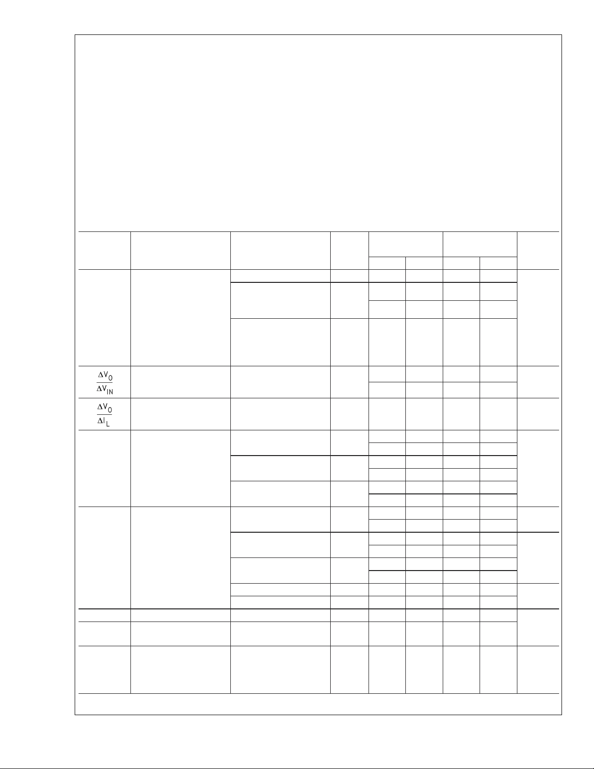
Electrical Characteristics
Limits in standard typeface are for TJ= 25˚C, and limits in boldface type apply over the full operating temperature range. Unless otherwise specified: V
(NOM) + 1V, IL= 1 mA, C
IN=VO
Symbol Parameter Conditions Typical
V
O
Output Voltage
Tolerance
1mA<I
(NOM) + 1V ≤ VIN≤
V
O
L
<
500 mA
16V
<
<
I
1mA
(NOM) + 1V ≤ VIN≤
V
O
L
500 mA
16V
−25˚C ≤ T
Output Voltage Line
Regulation
VO(NOM) + 1V ≤ VIN≤
16V
Load Regulation 1 mA<I
≤ 125˚C
J
<
500 mA 0.4 %V
L
= 4.7 µF, CIN= 2.2 µF, V
OUT
0.005
= 2V.
S/D
LP2989AI-X.X
(Note 6)
LP2989I-X.X
(Note 6)
Min Max Min Max
−0.75 0.75 −1.25 1.25
−1.5 1.5 −2.5 2.5
−4.0 2.5 −5.0 3.5
−3.5 2.5 −4.5 3.5
0.014 0.014
0.032 0.032
Protected
Units
%V
NOM
%/V
NOM
VIN–V
O
Dropout Voltage
IL= 100 µA
(Note 7)
= 200 mA
I
L
I
= 500 mA
L
I
GND
I
(PK) Peak Output Current V
O
I
(MAX) Short Circuit Current RL= 0 (Steady State)
O
Ground Pin Current IL= 100 µA
I
= 200 mA
L
I
= 500 mA
L
<
V
0.18V 0.5 2 2
S/D
<
V
0.4V 0.05 0.8 0.8
S/D
≥ VO(NOM) − 5% 800 600 600
OUT
(Note 9)
e
n
Output Noise Voltage
(RMS)
BW = 100 Hz to
100 kHz, C
C
BYPASS
V
OUT
OUT
= .01 µF
= 2.5V
=10µF
1
150
310
110
1
3
33
44
200 200
300 300
mV
425 425
650 650
175 175
200 200
µA
22
3.5 3.5
66
mA
99
µA
1000
mA
18 µV(RMS)
www.national.com 6
 Loading...