

LP2981
Micropower 100 mA Ultra Low-Dropout Regulator in
SOT-23 and micro SMD Packages
LP2981 Micropower 100 mA Ultra Low-Dropout Regulator in SOT-23 and micro SMD Packages
May 2005
General Description
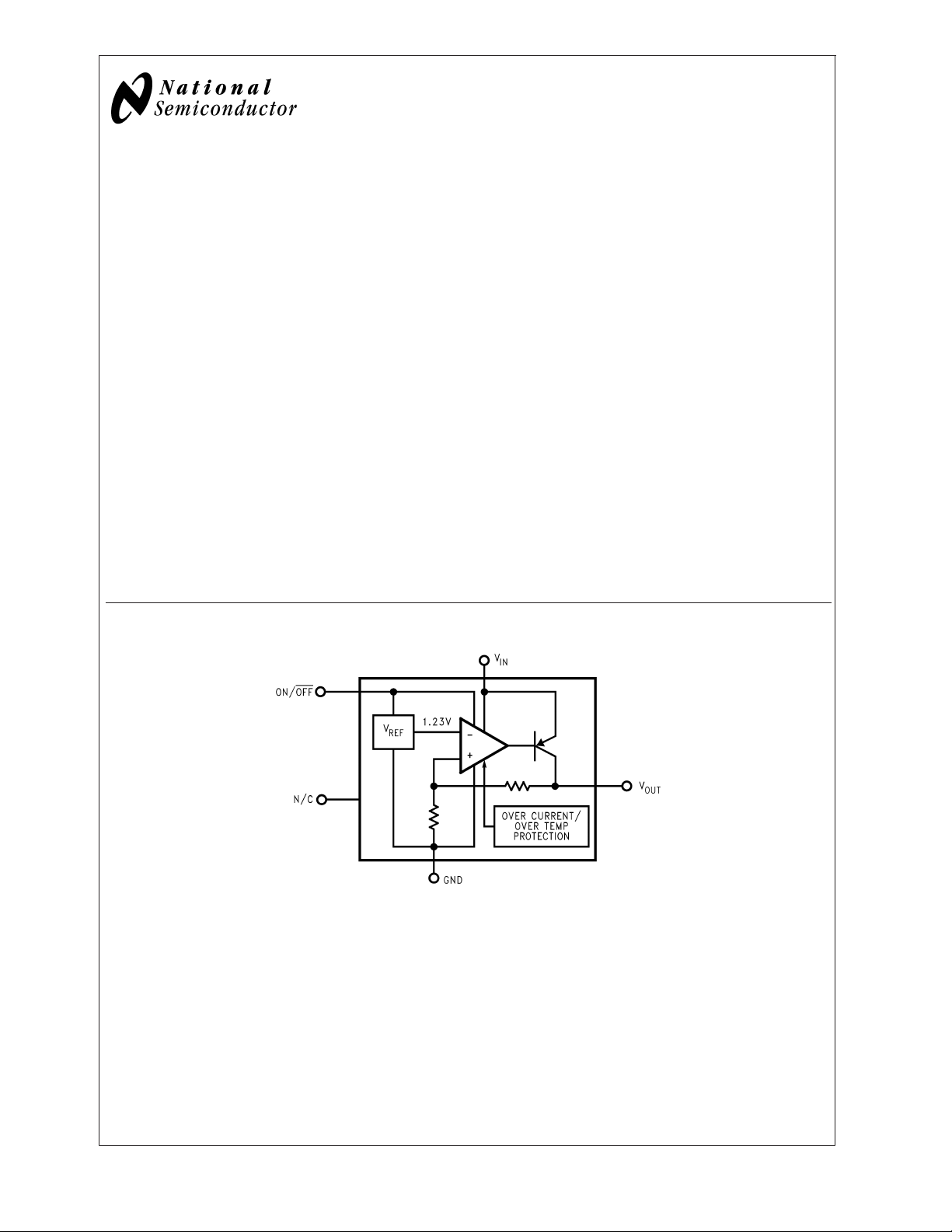
The LP2981 is a 100 mA, fixed-output voltage regulator
designed specifically to meet the requirements of batterypowered applications.
™
Using an optimized VIP
cess, the LP2981 delivers unequaled performance in all
specifications critical to battery-powered designs:
Dropout Voltage. Typically 200 mV
@
7mV
Ground Pin Current. Typically 600 µA
80 µA
Sleep Mode. Less than 1 µA quiescent current when ON/
OFF pin is pulled low.
Smallest Possible Size. SOT-23 and micro SMD packages
use an absolute minimum board space.
Precision Output. 0.75% tolerance output voltages avail-
able (A grade).
Eleven voltage options, from 2.5V to 5.0V, are available as
standard products.
1 mA load.
@
1 mA load.
(Vertically Integrated PNP) pro-
@
100 mA load, and
@
100 mA load, and
Block Diagram
Features
n Ultra low dropout voltage
n Output voltage accuracy 0.75% (A Grade)
n Guaranteed 100 mA output current
n Smallest possible size (SOT-23, micro SMD package)
<
n
1 µA quiescent current when shutdown
n Low ground pin current at all load currents
n High peak current capability (300 mA typical)
n Wide supply voltage range (16V max)
n Fast dynamic response to line and load
n Low Z
n Overtemperature/overcurrent protection
n −40˚C to +125˚C junction temperature range
over wide frequency range
OUT
Applications
n Cellular Phone
n Palmtop/Laptop Computer
n Personal Digital Assistant (PDA)
n Camcorder, Personal Stereo, Camera
01250601
VIP™is a trademark of National Semiconductor Corporation.
© 2005 National Semiconductor Corporation DS012506 www.national.com
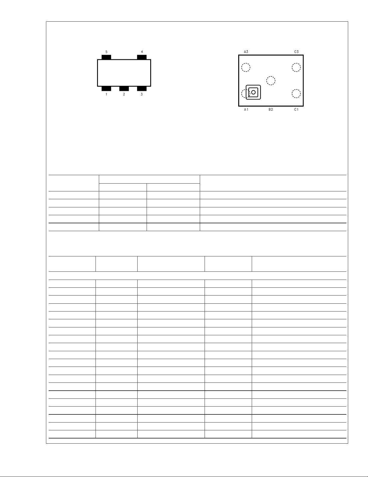
Connection Diagrams
LP2981
5-Lead Small Outline Package (M5) micro SMD, 5 Bump Package (BPA05)
Top View
01250602
See NS Package Number MF05A
For ordering information see Table 1
Note: The actual physical placement of the package marking will vary from
part to part. Package marking contains date code and lot traceability
information, and will vary considerably. Package marking does not correlate
to device type.
Top View
See NS Package Number BPA05
Pin Descrption
Name Pin Number Function
SOT-23 micro SMD
V
IN
1 C3 Input Voltage
GND 2 A1 Common Ground (device substrate)
ON/OFF 3 A3 Logic high enable input
N/C 4 B2 Post package trim - do not connect to this pin
V
OUT
5 C1 Regulated output voltage
Ordering Information
TABLE 1. Package Marking and Order Information
Output Voltage
(V)
5-Lead Small Outline Package (M5)
2.5 A LP2981AIM5X-2.5 L0CA 3000 Units on Tape and Reel
2.5 A LP2981AIM5-2.5 L0CA 1000 Units on Tape and Reel
2.5 STD LP2981IM5X-2.5 L0CB 3000 Units on Tape and Reel
2.5 STD LP2981IM5-2.5 L0CB 1000 Units on Tape and Reel
2.7 A LP2981AIM5X-2.7 L0DA 3000 Units on Tape and Reel
2.7 A LP2981AIM5-2.7 L0DA 1000 Units on Tape and Reel
2.7 STD LP2981IM5X-2.7 L0DB 3000 Units on Tape and Reel
2.7 STD LP2981IM5-2.7 L0DB 1000 Units on Tape and Reel
2.8 A LP2981AIM5X-2.8 L77A 3000 Units on Tape and Reel
2.8 A LP2981AIM5-2.8 L77A 1000 Units on Tape and Reel
2.8 STD LP2981IM5X-2.8 L77B 3000 Units on Tape and Reel
2.8 STD LP2981IM5-2.8 L77B 1000 Units on Tape and Reel
2.9 A LP2981AIM5X-2.9 L0VA 3000 Units on Tape and Reel
2.9 A LP2981AIM5-2.9 L0VA 1000 Units on Tape and Reel
2.9 STD LP2981IM5X-2.9 L0VB 3000 Units on Tape and Reel
2.9 STD LP2981IM5-2.9 L0VB 1000 Units on Tape and Reel
3.0 A LP2981AIM5X-3.0 L05A 3000 Units on Tape and Reel
3.0 A LP2981AIM5-3.0 L05A 1000 Units on Tape and Reel
3.0 STD LP2981IM5X-3.0 L05B 3000 Units on Tape and Reel
3.0 STD LP2981IM5-3.0 L05B 1000 Units on Tape and Reel
Grade Order Information Package
Marking
01250650
Supplied as:
www.national.com 2
Ordering Information (Continued)
TABLE 1. Package Marking and Order Information (Continued)
Output Voltage
(V)
3.1 A LP2981AIM5X-3.1 L38A 3000 Units on Tape and Reel
3.1 A LP2981AIM5-3.1 L38A 1000 Units on Tape and Reel
3.1 STD LP2981IM5X-3.1 L38B 3000 Units on Tape and Reel
3.1 STD LP2981IM5-3.1 L38B 1000 Units on Tape and Reel
3.2 A LP2981AIM5X-3.2 L35A 3000 Units on Tape and Reel
3.2 A LP2981AIM5-3.2 L35A 1000 Units on Tape and Reel
3.2 STD LP2981IM5X-3.2 L35B 3000 Units on Tape and Reel
3.2 STD LP2981IM5-3.2 L35B 1000 Units on Tape and Reel
3.3 A LP2981AIM5X-3.3 L04A 3000 Units on Tape and Reel
3.3 A LP2981AIM5-3.3 L04A 1000 Units on Tape and Reel
3.3 STD LP2981IM5X-3.3 L04B 3000 Units on Tape and Reel
3.3 STD LP2981IM5-3.3 L04B 1000 Units on Tape and Reel
3.6 A LP2981AIM5X-3.6 L0JA 3000 Units on Tape and Reel
3.6 A LP2981AIM5-3.6 L0JA 1000 Units on Tape and Reel
3.6 STD LP2981IM5X-3.6 L0JB 3000 Units on Tape and Reel
3.6 STD LP2981IM5-3.6 L0JB 1000 Units on Tape and Reel
3.8 A LP2981AIM5X-3.8 L36A 3000 Units on Tape and Reel
3.8 A LP2981AIM5-3.8 L36A 1000 Units on Tape and Reel
3.8 STD LP2981IM5X-3.8 L36B 3000 Units on Tape and Reel
3.8 STD LP2981IM5-3.8 L36B 1000 Units on Tape and Reel
4.0 A LP2981AIM5X-4.0 L0ZA 3000 Units on Tape and Reel
4.0 A LP2981AIM5-4.0 L0ZA 1000 Units on Tape and Reel
4.0 STD LP2981IM5X-4.0 L0ZB 3000 Units on Tape and Reel
4.0 STD LP2981IM5-4.0 L0ZB 1000 Units on Tape and Reel
4.7 A LP2981AIM5X-4.7 L0GA 3000 Units on Tape and Reel
4.7 A LP2981AIM5-4.7 L0GA 1000 Units on Tape and Reel
4.7 STD LP2981IM5X-4.7 L0GB 3000 Units on Tape and Reel
4.7 STD LP2981IM5-4.7 L0GB 1000 Units on Tape and Reel
5.0 A LP2981AIM5X-5.0 L03A 3000 Units on Tape and Reel
5.0 A LP2981AIM5-5.0 L03A 1000 Units on Tape and Reel
5.0 STD LP2981IM5X-5.0 L03B 3000 Units on Tape and Reel
5.0 STD LP2981IM5-5.0 L03B 1000 Units on Tape and Reel
micro SMD, 5 Bump Package (BPA05)
2.5 A LP2981AIBP-2.5 250 Units on Tape and Reel
2.5 A LP2981AIBPX-2.5 3000 Units on Tape and Reel
2.5 STD LP2981IBP-2.5 250 Units on Tape and Reel
2.5 STD LP2981IBPX-2.5 3000 Units on Tape and Reel
3.2 A LP2981AIBP-3.2 250 Units on Tape and Reel
3.2 A LP2981AIBPX-3.2 3000 Units on Tape and Reel
3.2 STD LP2981IBP-3.2 250 Units on Tape and Reel
3.2 STD LP2981IBPX-3.2 3000 Units on Tape and Reel
3.3 A LP2981AIBP-3.3 250 Units on Tape and Reel
3.3 A LP2981AIBPX-3.3 3000 Units on Tape and Reel
3.3 STD LP2981IBP-3.3 250 Units on Tape and Reel
3.3 STD LP2981IBPX-3.3 3000 Units on Tape and Reel
Grade Order Information Package
Marking
LP2981
Supplied as:
www.national.com3
Absolute Maximum Ratings (Note 1)
If Military/Aerospace specified devices are required,
LP2981
please contact the National Semiconductor Sales Office/
Distributors for availability and specifications.
Storage Temperature Range −65˚C to +150˚C
Operating Junction Temperature
Range −40˚C to +125˚C
Input Supply Voltage (Survival) −0.3V to +16V
Input Supply Voltage (Operating) 2.1V to +16V
Shutdown Input Voltage
(Survival) −0.3V to +16V
Output Voltage (Survival, (Note
4)) −0.3V to +9V
I
(Survival) Short Circuit
OUT
Lead Temperature
(Soldering, 5 sec.) 260˚C
ESD Rating (Note 2) 2 kV
Input-Output Voltage
(Survival, (Note 5) −0.3V to +16V
Power Dissipation (Note 3) Internally Limited
Electrical Characteristics (Note 10)
Limits in standard typeface are for TJ= 25˚C, and limits in boldface type applyover the full operating temperature range. Unless otherwise specified: V
IN=VO(NOM)
+ 1V, CIN= 1 µF, IL= 1 mA, C
Symbol Parameter Conditions Typ LP2981AI-XX LP2981I-XX Units
∆V
O
Output Voltage
IL= 1mA −0.75 0.75 −1.25 1.25
Tolerance
<
100 mA −1.0 1.0 −2.0 2.0
L
+ 1V 0.007 0.014 0.014 %/V
≤ 16V 0.032 0.032
IN
V
IN–VO
1mA<I
Output Voltage V
O(NOM)
Line Regulation ≤ V
Dropout Voltage IL=0 1 3 3 mV
(Note 7) 55
I
= 1 mA 7 10 10
L
I
= 25 mA 70 100 100
L
I
= 100 mA 200 250 250
L
I
GND
V
ON/OFF
Ground Pin Current IL= 0 65 95 95 µA
I
= 1 mA 80 110 110
L
I
= 25 mA 200 300 300
L
I
= 100 mA 600 800 800
L
ON/OFF
ON/OFF
<
0.3V 0.01 0.8 0.8
<
0.15V 0.05 2 2
V
V
ON/OFF Input Voltage High = O/P ON 1.4 1.6 1.6 V
(Note 8) Low = O/P OFF 0.50 0.15 0.15
I
ON/OFF
I
O(PK)
e
n
ON/OFF Input Current V
V
Peak Output Current V
= 0 0.01 −1 −1 µA
ON/OFF
=5V 5 15 15
ON/OFF
OUT
≥ V
− 5% 400 150 150 mA
O(NOM)
Output Noise BW = 300 Hz–50 kHz, 160 µV
Voltage (RMS) C
OUT
=10µF
Ripple Rejection f = 1 kHz 63 dB
C
=10µF
OUT
I
O(MAX)
Short Circuit Current RL= 0 (Steady State) 150 mA
OUT
= 4.7 µF,V
ON/OFF
= 2V.
(Note 6) (Note 6)
Min Max Min Max
−2.5 2.5 −3.5 3.5
15 15
150 150
375 375
125 125
170 170
550 550
1500 1500
Protected
%V
NOM
www.national.com 4
Electrical Characteristics (Note 10) (Continued)
Limits in standard typeface are for TJ= 25˚C, and limits in boldface type applyover the full operating temperature range. Unless otherwise specified: V
IN=VO(NOM)
+ 1V, CIN= 1 µF, IL= 1 mA, C
Symbol Parameter Conditions Typ LP2981AI-XX LP2981I-XX Units
(Note 9)
Note 1: Absolute maximum ratings indicate limits beyond which damage to the component may occur. Electrical specifications do not apply when operating the
device outside of its rated operating conditions.
Note 2: The ESD rating of pins 3 and 4 for the SOT-23 package, or pins 5 and 2 for the micro SMD package, is 1 kV.
Note 3: The maximum allowable power dissipation is a function of the maximum junction temperature, T
the ambient temperature, T
The value of θJAfor the SOT-23 package is 220˚C/W and the micro SMD package is 225˚C/W. Exceeding the maximum allowable power dissipation will cause
excessive die temperature, and the regulator will go into thermal shutdown.
Note 4: If used in a dual-supply system where the regulator load is returned to a negative supply, the LP2981 output must be diode-clamped to ground.
Note 5: The output PNP structure contains a diode between the V
will turn on this diode (see Application Hints).
Note 6: Limits are 100% production tested at 25˚C. Limits over the operating temperature range are guaranteed through correlation using Statistical Quality Control
(SQC) methods. The limits are used to calculate National’s Average Outgoing Quality Level (AOQL).
Note 7: Dropout voltage is defined as the input to output differential at which the output voltage drops 100 mV below the value measured with a 1V differential.
Note 8: The ON/OFF inputs must be properly driven to prevent misoperation. For details, refer to Application Hints.
Note 9: See Typical Performance Characteristics curves.
Note 10: Exposing the micro SMD device to direct sunlight will cause misoperation. See Application Hints for additional information.
. The maximum allowable power dissipation at any ambient temperature is calculated using:
A
IN
and V
terminals that is normally reverse-biased. Reversing the polarity from VINto V
OUT
OUT
= 4.7 µF,V
ON/OFF
= 2V.
(Note 6) (Note 6)
Min Max Min Max
, the junction-to-ambient thermal resistance, θJA, and
J(MAX)
OUT
LP2981
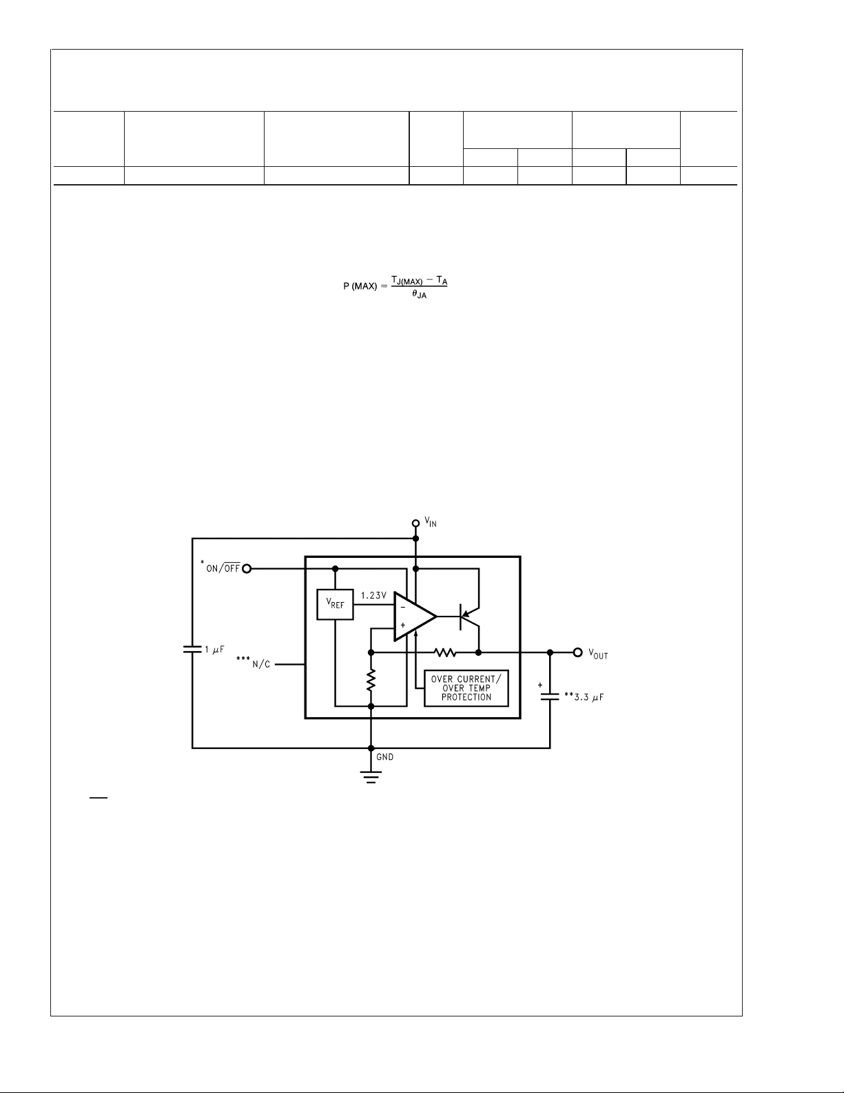
Basic Application Circuit
*
ON/OFF input must be actively terminated. Tie to VINif this function is not to be used.
**
Minimum Output Capacitance is shown to insure stability over full load current range. More capacitance provides superior dynamic performance and
additional stability margin (see Application Hints).
***
Do not make connections to this pin.
01250604
www.national.com5
 Loading...