

LP2980
Micropower 50 mA Ultra Low-Dropout Regulator
LP2980 Micropower 50 mA Ultra Low-Dropout Regulator
April 2000
General Description
The LP2980 is a 50 mA, fixed-output voltage regulator designed specifically to meet the requirements of
battery-powered applications.
Using an optimized VIP
cess, the LP2980 delivers unequaled performance in all
specifications critical to battery-powered designs:
Dropout Voltage. Typically 120mV
@
1 mA load.
Ground PinCurrent. Typically375 µA
@
µA
1 mA load.
Sleep Mode. Less than 1 µA quiescent current when ON/
OFF pin is pulled low.
Smallest Possible Size. SOT-23 and micro SMD packages
use an absolute minimum board space.
Minimum Part Count. Requires only 1 µF of external capacitance on the regulator output.
Precision Output. 0.5% tolerance output voltages available
(A grade).
5.0V, 3.3V, and 3.0V versions available as standard products.
™
(Vertically Integrated PNP) pro-
@
50 mAload, and7 mV
@
50 mAload, and80
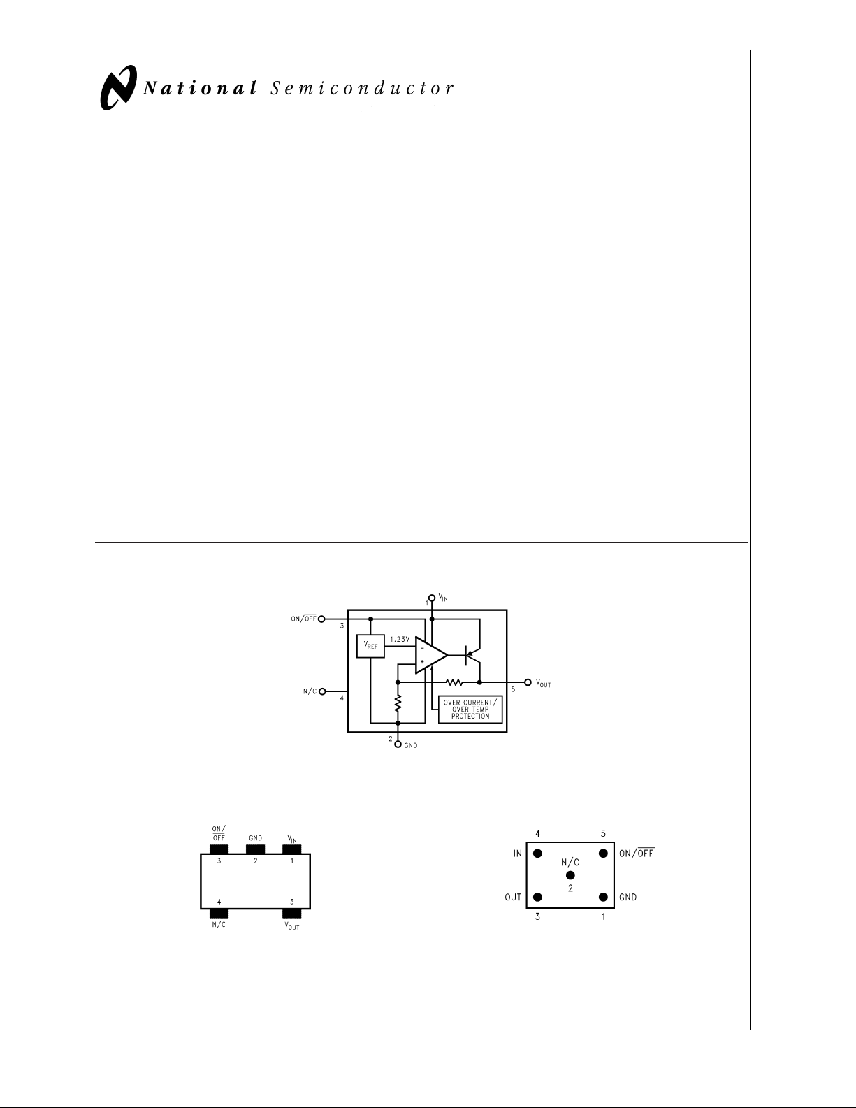
Block Diagram
Features
n Ultra low dropout voltage
n Output voltage accuracy 0.5% (A Grade)
n Guaranteed 50 mA output current
n Smallest possible size (SOT-23, micro SMD package)
n Requires only 1 µF external capacitance
<
n
1 µA quiescent current when shutdown
n Low ground pin current at all load currents
n High peak current capability (150 mA typical)
n Wide supply voltage range (16V max)
n Fast dynamic response to line and load
n Low Z
n Overtemperature/overcurrent protection
n −40˚C to +125˚C junction temperature range
over wide frequency range
OUT
Applications
n Cellular Phone
n Palmtop/Laptop Computer
n Personal Digital Assistant (PDA)
n Camcorder, Personal Stereo, Camera
DS012078-1
Connection Diagram and Ordering Information
5-Lead Small Outline Package (M5)
DS012078-3
Top View
See NS Package Number MF05A
For ordering information see
VIP™is a trademark of National Semiconductor Corporation.
© 2000 National Semiconductor Corporation DS012078 www.national.com
Table 1
micro SMD, 5 Bump Package (BPA05)
DS012078-60
Bottom View
See NS Package Number BPA05
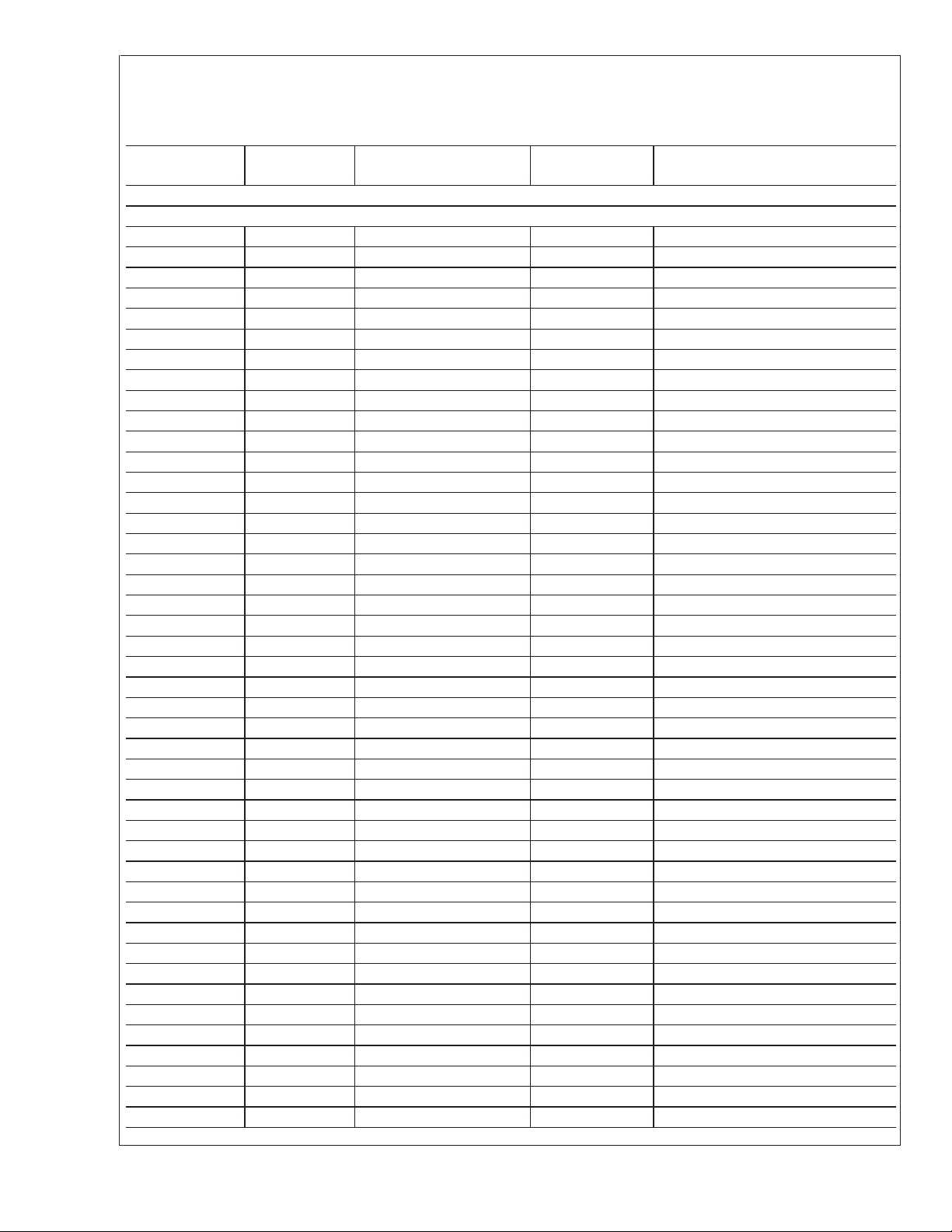
Ordering Information
LP2980
TABLE 1. Package Marking and Order Information
Output Voltage
(V)
5-Lead Small Outline Package (M5)
For output voltages ≤ 2V, refer to LP2980LV datasheet. If a non-standard voltage is required, see LP2980-ADJ.
2.5 A LP2980AIM5X-2.5 L0NA 3000 Units on Tape and Reel
2.5 A LP2980AIM5-2.5 L0NA 1000 Units on Tape and Reel
2.5 STD LP2980IM5X-2.5 L0NB 3000 Units on Tape and Reel
2.5 STD LP2980IM5-2.5 L0NB 1000 Units on Tape and Reel
2.6 A LP2980AIM5X-2.6 L48A 3000 Units on Tape and Reel
2.6 A LP2980AIM5-2.6 L48A 1000 Units on Tape and Reel
2.6 STD LP2980IM5X-2.6 L48B 3000 Units on Tape and Reel
2.6 STD LP2980IM5-2.6 L48B 1000 Units on Tape and Reel
2.7 A LP2980AIM5X-2.7 L26A 3000 Units on Tape and Reel
2.7 A LP2980AIM5-2.7 L26A 1000 Units on Tape and Reel
2.7 STD LP2980IM5X-2.7 L26B 3000 Units on Tape and Reel
2.7 STD LP2980IM5-2.7 L26B 1000 Units on Tape and Reel
2.8 A LP2980AIM5X-2.8 L13A 3000 Units on Tape and Reel
2.8 A LP2980AIM5-2.8 L13A 1000 Units on Tape and Reel
2.8 STD LP2980IM5X-2.8 L13B 3000 Units on Tape and Reel
2.8 STD LP2980IM5-2.8 L13B 1000 Units on Tape and Reel
2.9 A LP2980AIM5X-2.9 L12A 3000 Units on Tape and Reel
2.9 A LP2980AIM5-2.9 L12A 1000 Units on Tape and Reel
2.9 STD LP2980IM5X-2.9 L12B 3000 Units on Tape and Reel
2.9 STD LP2980IM5-2.9 L12B 1000 Units on Tape and Reel
3.0 A LP2980AIM5X-3.0 L02A 3000 Units on Tape and Reel
3.0 A LP2980AIM5-3.0 L02A 1000 Units on Tape and Reel
3.0 STD LP2980IM5X-3.0 L02B 3000 Units on Tape and Reel
3.0 STD LP2980IM5-3.0 L02B 1000 Units on Tape and Reel
3.1 A LP2980AIM5X-3.1 L30A 3000 Units on Tape and Reel
3.1 A LP2980AIM5-3.1 L30A 1000 Units on Tape and Reel
3.1 STD LP2980IM5X-3.1 L30B 3000 Units on Tape and Reel
3.1 STD LP2980IM5-3.1 L30B 1000 Units on Tape and Reel
3.2 A LP2980AIM5X-3.2 L31A 3000 Units on Tape and Reel
3.2 A LP2980AIM5-3.2 L31A 1000 Units on Tape and Reel
3.2 STD LP2980IM5X-3.2 L31B 3000 Units on Tape and Reel
3.2 STD LP2980IM5-3.2 L31B 1000 Units on Tape and Reel
3.3 A LP2980AIM5X-3.3 L00A 3000 Units on Tape and Reel
3.3 A LP2980AIM5-3.3 L00A 1000 Units on Tape and Reel
3.3 STD LP2980IM5X-3.3 L00B 3000 Units on Tape and Reel
3.3 STD LP2980IM5-3.3 L00B 1000 Units on Tape and Reel
3.5 A LP2980AIM5X-3.5 L27A 3000 Units on Tape and Reel
3.5 A LP2980AIM5-3.5 L27A 1000 Units on Tape and Reel
3.5 STD LP2980IM5X-3.5 L27B 3000 Units on Tape and Reel
3.5 STD LP2980IM5-3.5 L27B 1000 Units on Tape and Reel
3.6 A LP2980AIM5X-3.6 L28A 3000 Units on Tape and Reel
3.6 A LP2980AIM5-3.6 L28A 1000 Units on Tape and Reel
3.6 STD LP2980IM5X-3.6 L28B 3000 Units on Tape and Reel
3.6 STD LP2980IM5-3.6 L28B 1000 Units on Tape and Reel
Grade Order Information Package
Marking
Supplied as:
www.national.com 2
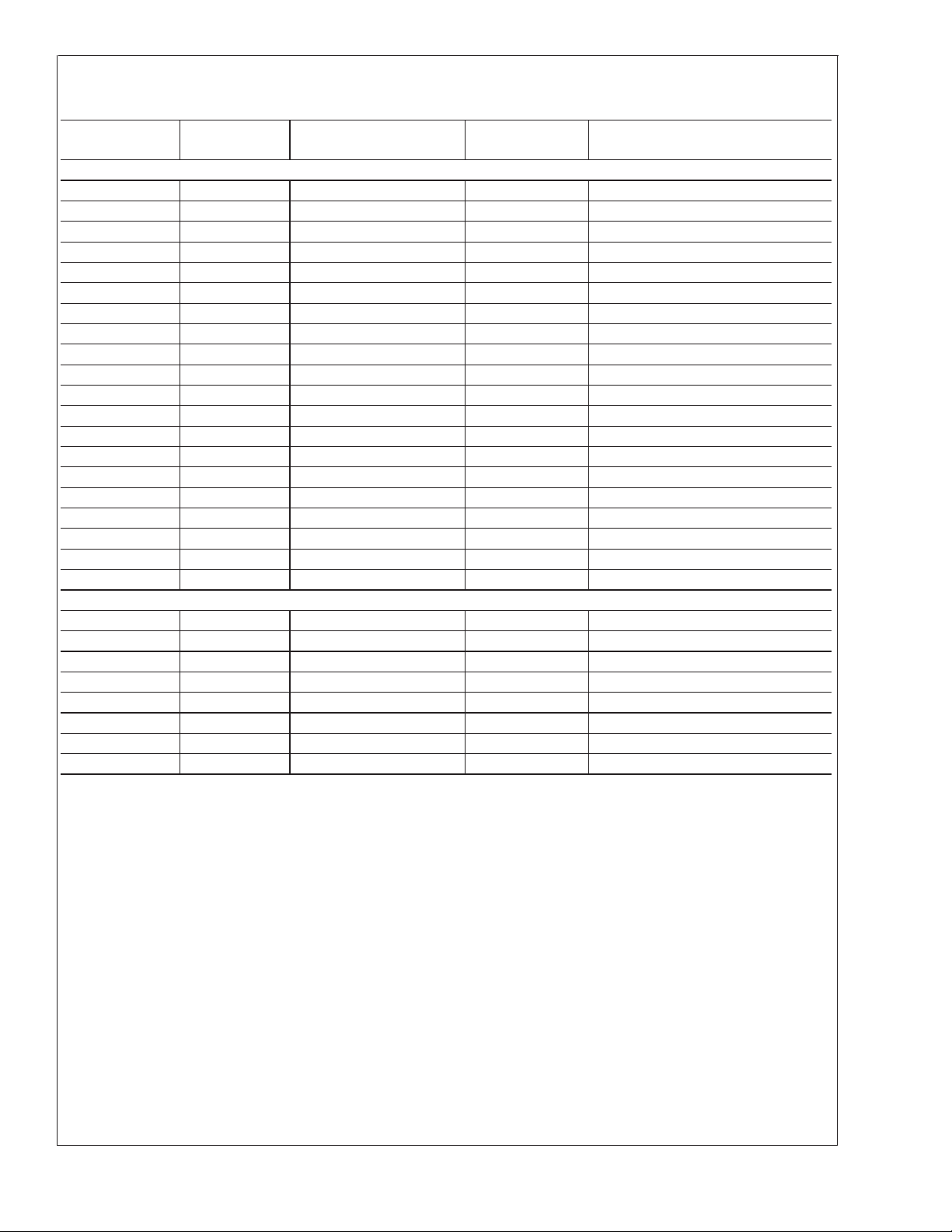
Ordering Information (Continued)
TABLE 1. Package Marking and Order Information (Continued)
Output Voltage
(V)
For output voltages ≤ 2V, refer to LP2980LV datasheet. If a non-standard voltage is required, see LP2980-ADJ.
3.8 A LP2980AIM5X-3.8 L21A 3000 Units on Tape and Reel
3.8 A LP2980AIM5-3.8 L21A 1000 Units on Tape and Reel
3.8 STD LP2980IM5X-3.8 L21B 3000 Units on Tape and Reel
3.8 STD LP2980IM5-3.8 L21B 1000 Units on Tape and Reel
4.0 A LP2980AIM5X-4.0 L25A 3000 Units on Tape and Reel
4.0 A LP2980AIM5-4.0 L25A 1000 Units on Tape and Reel
4.0 STD LP2980IM5X-4.0 L25B 3000 Units on Tape and Reel
4.0 STD LP2980IM5-4.0 L25B 1000 Units on Tape and Reel
4.5 A LP2980AIM5X-4.5 L0XA 3000 Units on Tape and Reel
4.5 A LP2980AIM5-4.5 L0XA 1000 Units on Tape and Reel
4.5 STD LP2980IM5X-4.5 L0XB 3000 Units on Tape and Reel
4.5 STD LP2980IM5-4.5 L0XB 1000 Units on Tape and Reel
4.7 A LP2980AIM5X-4.7 L37A 3000 Units on Tape and Reel
4.7 A LP2980AIM5-4.7 L37A 1000 Units on Tape and Reel
4.7 STD LP2980IM5X-4.7 L37B 3000 Units on Tape and Reel
4.7 STD LP2980IM5-4.7 L37B 1000 Units on Tape and Reel
5.0 A LP2980AIM5X-5.0 L01A 3000 Units on Tape and Reel
5.0 A LP2980AIM5-5.0 L01A 1000 Units on Tape and Reel
5.0 STD LP2980IM5X-5.0 L01B 3000 Units on Tape and Reel
5.0 STD LP2980IM5-5.0 L01B 1000 Units on Tape and Reel
micro SMD, 5 Bump Package (BPA05)
3.3 A LP2980AIBP-3.3 250 Units on Tape and Reel
3.3 A LP2980AIBPX-3.3 3000 Units on Tape and Reel
3.3 STD LP2980IBP-3.3 250 Units on Tape and Reel
3.3 STD LP2980IBPX-3.3 3000 Units on Tape and Reel
5.0 A LP2980AIBP-5.0 250 Units on Tape and Reel
5.0 A LP2980AIBPX-5.0 3000 Units on Tape and Reel
5.0 STD LP2980IBP-5.0 250 Units on Tape and Reel
5.0 STD LP2980IBPX-5.0 3000 Units on Tape and Reel
Grade Order Information Package
Marking
Supplied as:
LP2980
www.national.com3
Absolute Maximum Ratings (Note 1)
If Military/Aerospace specified devices are required,
LP2980
please contact the National Semiconductor SalesOffice/
Distributors for availability and specifications.
Storage Temperature Range −65˚C to +150˚C
Operating Junction Temperature
Range −40˚C to +125˚C
Lead Temperature
(Soldering, 5 sec.) 260˚C
ESD Rating (Note 2) 2 kV
Power Dissipation (Note 3) Internally Limited
Input Supply Voltage (Survival) −0.3V to +16V
Input Supply Voltage (Operating) 2.1V to +16V
Shutdown Input Voltage (Survival) −0.3V to +16V
Output Voltage (Survival), (Note 4) −0.3V to +9V
(Survival) Short Circuit Protected
I
OUT
Input-Output Voltage (Survival),
(Note 5) −0.3V to +16V
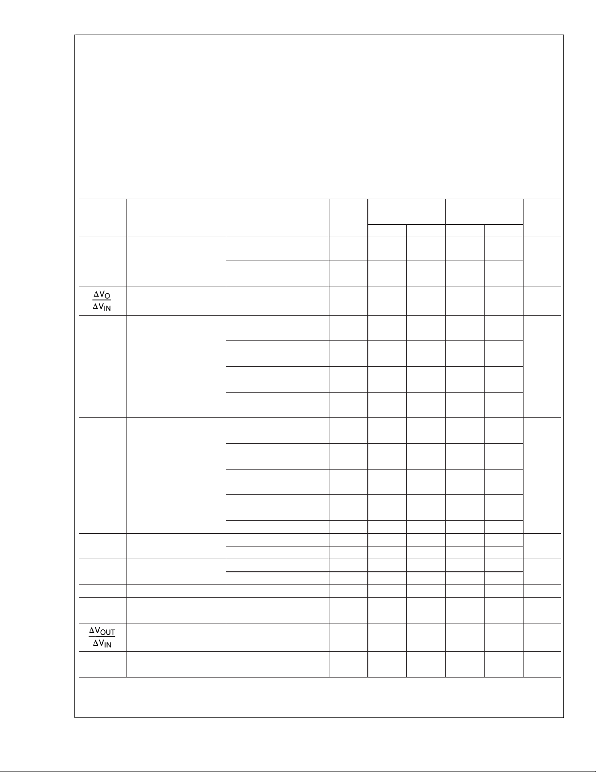
Electrical Characteristics
Limits in standard typeface are for TJ= 25˚C, and limits in boldface type apply over the full operating temperature range. Unless otherwise specified: VIN=V
Symbol Parameter Conditions Typ LP2980AI-XX LP2980I-XX Units
∆V
O
Output Voltage
Tolerance
Output Voltage V
Line Regulation ≤ V
V
IN–VO
Dropout Voltage IL=0 133mV
(Note 7) 55
I
GND
V
ON/OFF
Ground Pin Current IL= 0 65 95 95 µA
ON/OFF Input Voltage High = O/P ON 1.4 1.6 1.6 V
(Note 8) Low = O/P OFF 0.55 0.18 0.18
I
ON/OFF
I
O(PK)
e
n
ON/OFF Input Current V
Peak Output Current V
Output Noise BW = 300 Hz–50 kHz, 160 µV
Voltage (RMS) C
Ripple Rejection f = 1 kHz
I
O(MAX)
Note 1: Absolute maximum ratings indicate limits beyond which damageto the component may occur. Electrical specifications do notapply when operating the device outside of its rated operating conditions.
Note 2: The ESD rating of pins 3 and 4 is 1 kV.
Short Circuit Current RL= 0 (Steady State) 150 mA
+ 1V, IL= 1 mA, C
O(NOM)
OUT
= 1 µF, V
ON/OFF
= 2V.
(Note 6) (Note 6)
Min Max Min Max
IL= 1 mA −0.50 0.50 −1.0 1.0
1mA<I
<
50 mA −0.75 0.75 −1.5 1.5
L
−2.5 2.5 −3.5 3.5
+1V
O(NOM)
≤ 16V 0.032 0.032
IN
I
= 1 mA 7 10 10
L
0.007
0.014 0.014
15 15
I
=10mA 406060
L
90 90
I
= 50 mA 120 150 150
L
225 225
125 125
I
= 1 mA 80 110 110
L
170 170
I
= 10 mA 140 220 220
L
460 460
I
= 50 mA 375 600 600
L
1200 1200
V
V
<
ON/OFF
ON/OFF
ON/OFF
OUT
OUT
0.18V 0 11
=0 0 −1 −1 µA
=5V 5 15 15
≥ V
− 5% 150 100 100 mA
O(NOM)
=10µF
63 dB
C
=10µF
OUT
(Note 9)
%V
NOM
%/V
www.national.com 4
Electrical Characteristics (Continued)
Note 3: The maximum allowablepower dissipationis a function of the maximum junction temperature, T
the ambient temperature, T
The value of θJAfor the SOT-23 package is 220˚C/W and the micro SMD package is 320˚C/W. Exceeding the maximum allowable power dissipation will cause excessive die temperature, and the regulator will go into thermal shutdown.
Note 4: If used in a dual-supply system where the regulator load is returned to a negative supply, the LP2980 output must be diode-clamped to ground.
Note 5: The output PNP structure contains a diode between the V
will turn on this diode (see Application Hints).
Note 6: Limits are 100%production testedat 25˚C. Limits over the operating temperature range are guaranteed throughcorrelation usingStatistical Quality Control
(SQC) methods. The limits are used to calculate National’sAverage Outgoing Quality Level (AOQL).
Note 7: Dropout voltage is defined as the input to output differential at which the output voltage drops 100 mV below the value measured with a 1V differential.
Note 8: The ON/OFF inputs must be properly driven to prevent misoperation. For details, refer to Application Hints.
Note 9: See Typical Performance Characteristics curves.
. The maximum allowable power dissipation at any ambient temperature is calculated using:
A
IN
and V
terminals that is normally reverse-biased. Reversing the polarity from VINto V
OUT
, thejunction-to-ambient thermalresistance, θJA, and
J(MAX)
OUT
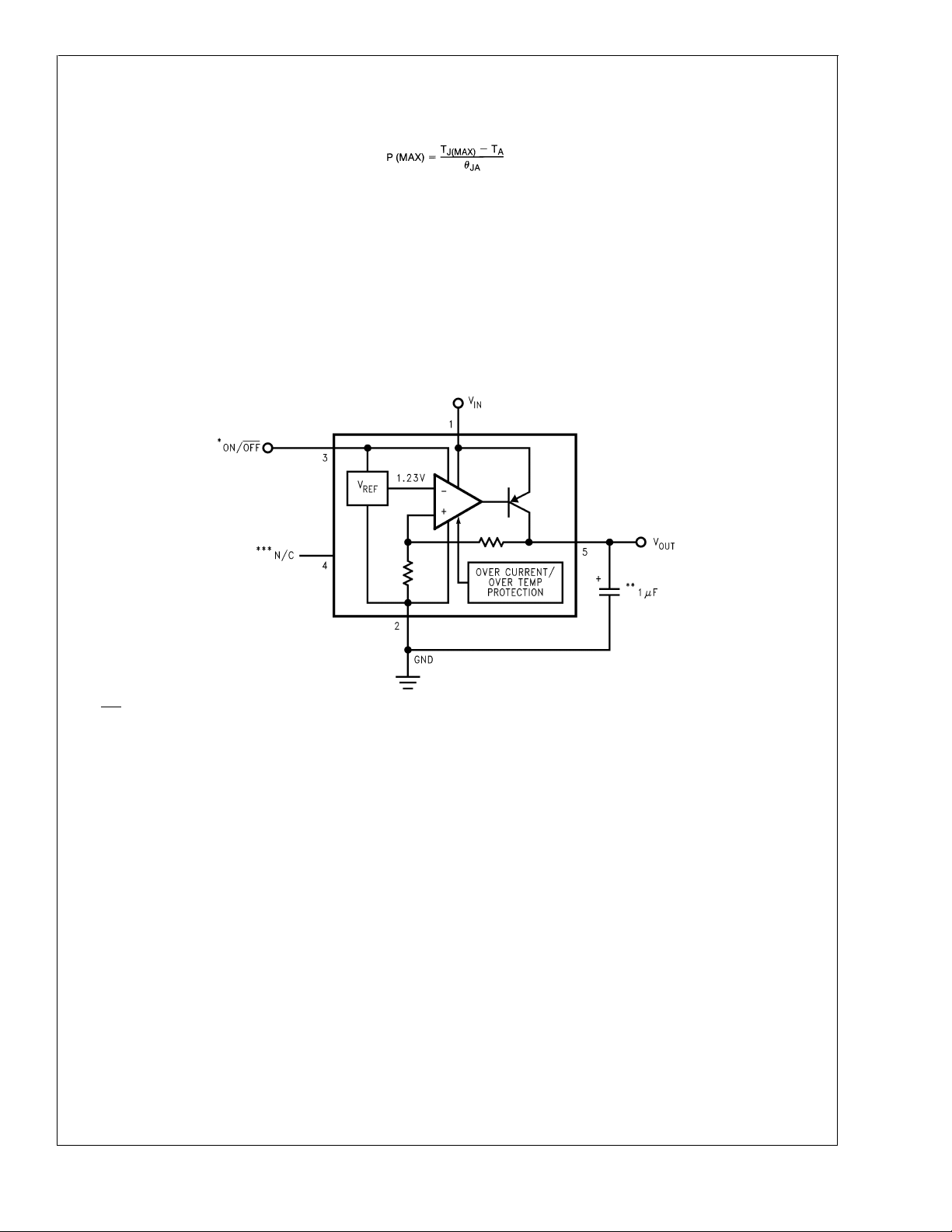
Basic Application Circuit
LP2980
DS012078-2
*
ON/OFF input must be actively terminated. Tie to VINif this function is not to be used.
**
Minimum Output Capacitance is 1 µF to insure stability over full load current range. More capacitance provides superior dynamic performance and additional
stability margin (seeApplication Hints).
***
Do not make connections to this pin.
www.national.com5
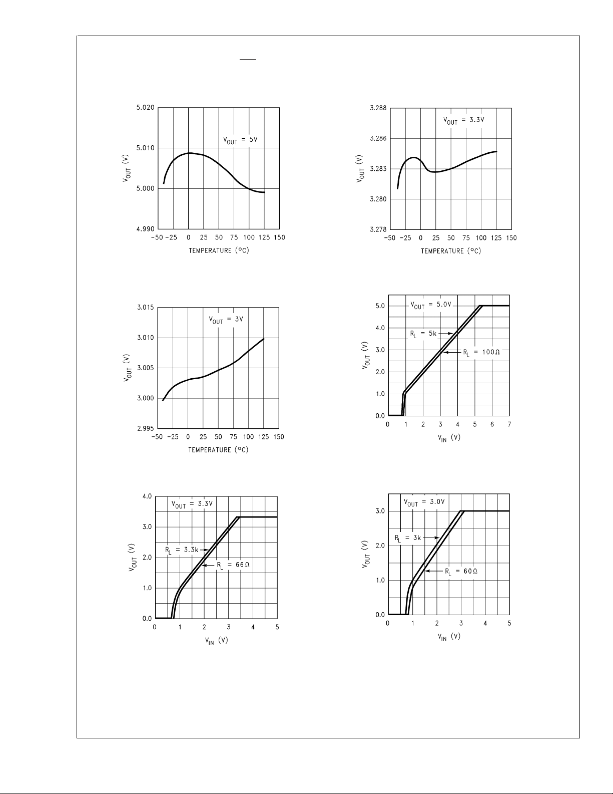
Typical Performance Characteristics Unless otherwise specified: T
C
= 2.2 µF, all voltage options, ON/OFF pin tied to VIN.
OUT
LP2980
= 25˚C, VIN=V
A
O(NOM)
+1V,
Output Voltage vs
Temperature
Output Voltage vs
Temperature
DS012078-9
Output Voltage vs
Temperature
DS012078-39
Dropout Characteristics
Dropout Characteristics
DS012078-40
DS012078-15
DS012078-16
Dropout Characteristics
DS012078-14
www.national.com 6
 Loading...