

LMX9820A
Bluetooth
®
Seria l Port Modul e
LMX9820A Bluetooth Serial Port Module
APRIL 2005
Revision 1.0
1.0 General Description
The National Semiconductor LMX9820A Bluetooth Serial
Port module is a highly integrated radio, baseband controller, and memory device implemented on an FR4 substrate.
All hardware and firmware is included to provide a complete solution from antenna from the complete lower and
upper layers of the Bluetooth stack, up to the application
support layers including the Generic Access Profile (GAP),
the Service Discovery Application Profile (SDAP), and the
Serial Port Profile (SPP). The module includes a configurable service database to fulfill service requests for additional profiles on the host. The LMX9820A features a small
form factor (10.1 x 14.1 x 2.0 mm) design, which solves
many of the challenges associated with compact system
integration. Moreover, the LMX9820A is pre-qualified as a
Bluetooth Integrated Component. Conformance testing
through the Bluetooth qualification program enables a fast
time to market after system integration by ensuring a high
degree of compliance and interoperability.
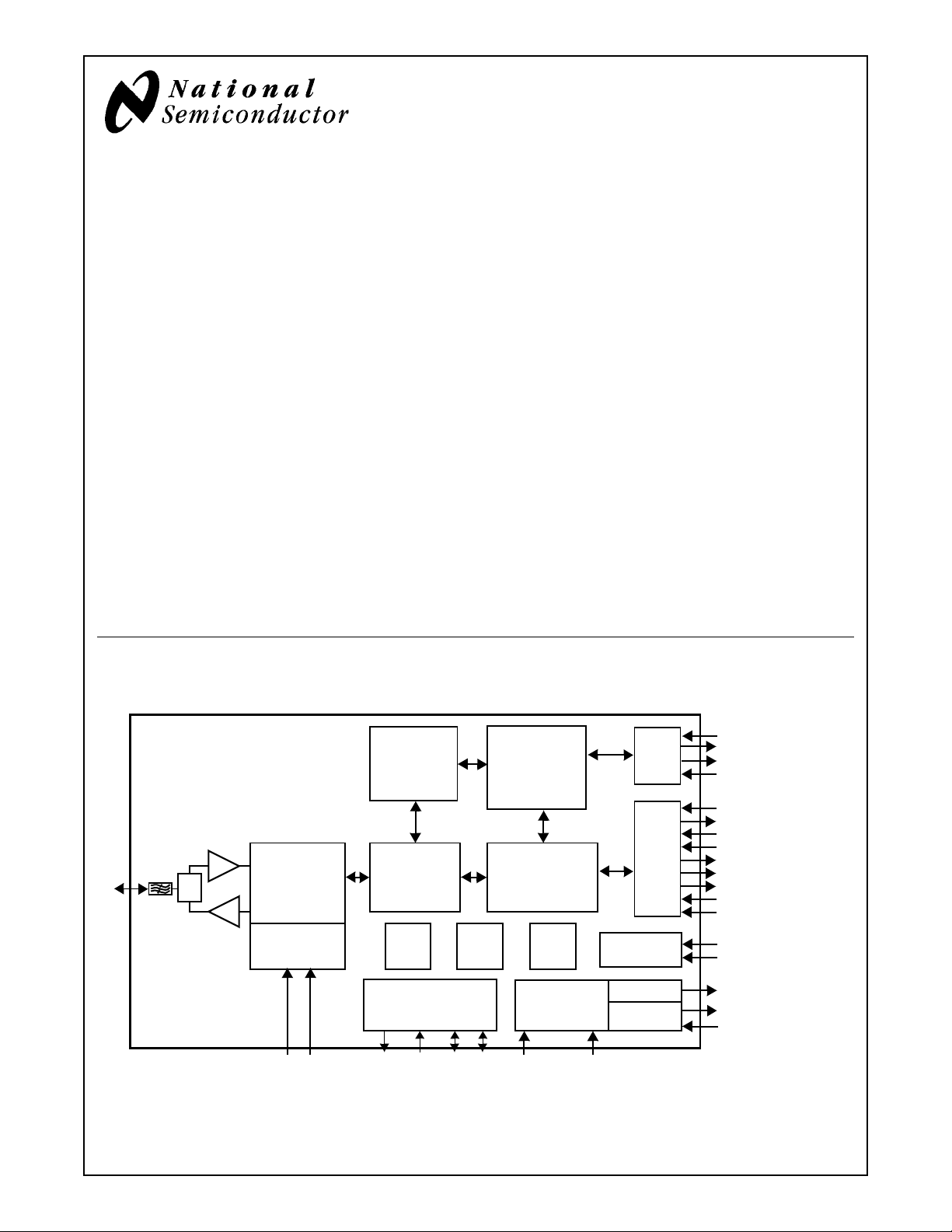
2.0 Functional Block Diagram
Based on National’s CompactRISC
™
16-bit processor
architecture and Digital Smart Radio technology, the
LMX9820A is optimized to handle the data and link management processing requirements of a Blueto oth node.
The firmware supplied with this device offers a complete
Bluetooth (v1.1) stack including profiles and command
interface. This firmware features point-to-point and pointto-multipoint link management supporting data rates up to
the theoretical maximum over RFComm of 704 kbps. The
internal memory supports up to three active Bluetooth data
links and one active SCO link .
1.1 APPLICATIONS
■ Personal Digital Assistants
■ POS Terminals
■ Data Logging Systems
■ Audio Gateway applicati ons
LINK
MGMNT
PROCESSOR
(LMP)
LNA
TR
ANTENNA
CompactRISC is a trademark of National Semiconductor Corporation.
Bluetooth is a registered trademark of Bluetooth SIG, Inc. and is used under license by National Semiconductor.
SW
PA
DIGITAL
SMART
RADIO
SYNTHESIZER
CRYSTAL/OSCILLATOR
BASEBAND
CONTROLLER
AUDIO INTERFACE
AAI_STD
AAI_SRD
ADVANCED
AAI_SFS
AAI_SCLK
FIRMWARE
(INCLUDES
PROFILES AND
COMMAND
INTERFACE)
COMPACTRISC™
CORE
JTAGRAMFLASH
VOLTAGE
REGULATORS
UART_RX
UART
AUX
PORTS
SELECT
ANALOG
DIGITAL
DIG_GND[1:2]VCC
UART_TX
UART_RTS#
UART_CTS#
IOVCC
TX_SWITCH_P
ENV0
ENV1
LSTAT_0
LSTAT_1
HOST_WU
RESET_B#
RESET_5100#
ISEL1INTERFACE
ISEL2
VDD_ANA_OUT
VDD_DIG_OUT
VDD_DIG_PWR_D#
© 2005 Nat ional Semiconductor Corpora tion www.national.com
3.0 Features
■ Bluetooth version 1.1 qualified
■ Implemented in CMOS technology on FR4 substrat e
■ Temperature Range: -40°C to +85°C
■ FCC certified on LMX9820ADONGLE,
FCC ID ED9LMX9820ASM.
3.1 DIGITAL HARDW ARE
■ Baseband and Link Management processors
■ CompactRISC Core
■ Integrated Memory:
–Flash
–RAM
■ UART Command/Data Port:
– Support for up to 921.6k baud rate
■ Auxiliary Host Interface Ports:
LMX9820A Bluetooth Serial Port Module
– Link Status
– Transceive r Status (Tx or Rx)
– Operating Environm ent Control:
– Default Bluetooth mode
– In System Programming (ISP) mode
■ Advanced Power Management (APM) features
■ Advanced Audio Interface for external PCM codec
3.2 FIRMWARE
■ Complete Bluetooth Stack including:
– Baseband and Link Manager
– L2CAP, RFCOMM, SDP
–Profiles:
–GAP
–SDAP
– SPP
■ Additional Profile support on host fo r any SPP based
profile, like
– Dial Up Networking (DUN)
– Facsimile Profile (FAX)
– File Transfer Protocol (FTP)
– Object Push Profile (OPP)
– Headset (HSP)
– Handsfree Profile (HFP)
■ On-chip application support including:
– Command Interface:
– Link setup and configuration (also Multipoint)
– Configuration of the module
– In-System Programming (ISP)
– Service database modifications
– Default connections
– UART Transparent mode
– Different Operation modes:
– Automatic mode
– Command mode
3.3 DIGITAL SMART RADIO
■ Accepts external clock or crystal input:
– 12 MHz
– 20 ppm cumulative clock error required for Bluetooth
■ Synthesizer:
– Integrated VCO and loop filter
– Provides all clocking f or radio and baseband func-
tions
■ Antenna Port (50 ohms nominal impedance):
– Embedded front-end filter for enhanced out of band
performance
■ Integrated transmit/ receive switch (full-duplex operation
via antenna port)
■ Typical -81 dBm input sensitivity
■ 0 dBm typical output power
3.4 PHYSICAL DIMENSIONS
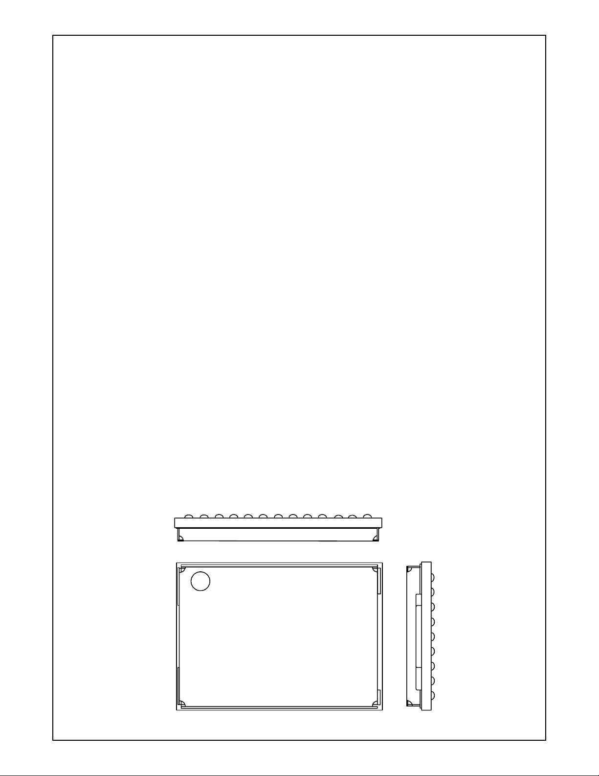
■ Compact size: 10.1mm x 14.1mm x 2.0mm
■ Complete system interface provi ded in Land Grid Array
on underside for surface-mount assembly
■ Metal shield included
Figure 1. Physical Illustrati o n
www.national.com 2 Revision 1.0

Table of Cont ents
LMX9820A Bluetooth Serial Port Module
1.0 General Description . . . . . . . . . . . . . . . . . . . . . . . . . . . .1
1.1 APPLICATIONS . . . . . . . . . . . . . . . . . . . . . . . . . . .1
2.0 Functional Block Diagram . . . . . . . . . . . . . . . . . . . . . . . 1
3.0 Features . . . . . . . . . . . . . . . . . . . . . . . . . . . . . . . . . . . . . .2
3.1 DIGITAL HARDWARE . . . . . . . . . . . . . . . . . . . . . . 2
3.2 FIRMWARE . . . . . . . . . . . . . . . . . . . . . . . . . . . . . . 2
3.3 DIGITAL SMART RADIO . . . . . . . . . . . . . . . . . . . . 2
3.4 PHYSICAL DIMENSIONS . . . . . . . . . . . . . . . . . . .2
4.0 Connection Diagram . . . . . . . . . . . . . . . . . . . . . . . . . . . . 4
5.0 Pad Descriptions . . . . . . . . . . . . . . . . . . . . . . . . . . . . . . 5
6.0 Electrical Specifications . . . . . . . . . . . . . . . . . . . . . . . .8
6.1 GENERAL SPECIFICATIONS . . . . . . . . . . . . . . . .8
6.2 DC CHARACTERISTICS . . . . . . . . . . . . . . . . . . . . 9
6.3 RF PERFORMANCE CHARACTERISTICS . . . .10
6.4 PERFORMANCE DATA (TYPICAL) . . . . . . . . . .12
7.0 Functional Description . . . . . . . . . . . . . . . . . . . . . . . . . 14
7.1 BASEBAND AND LINK MANAGEMENT
PROCESSORS 14
7.1.1 Bluetooth Lower Link Controller . . . . . . . . . . . .14
7.1.2 Bluetooth Upper Layer Stack . . . . . . . . . . . . . . 14
7.1.3 Profile Support . . . . . . . . . . . . . . . . . . . . . . . . . 14
7.1.4 Application with Command Interface . . . . . . . .14
7.2 MEMORY . . . . . . . . . . . . . . . . . . . . . . . . . . . . . . .15
7.3 CONTROL AND TRANSPORT PORT . . . . . . . . . 15
7.4 AUXILIARY PORTS . . . . . . . . . . . . . . . . . . . . . . . 15
7.4.1 Reset_5100 and Reset_b# . . . . . . . . . . . . . . .15
7.4.2 Operating Environment Pads (Env0 and Env1) 15
7.4.3 Interface Select Inputs (ISEL1, ISEL2) . . . . . .15
7.4.4 Module and LInk Status Outputs . . . . . . . . . . . 15
7.5 AUDIO PORT . . . . . . . . . . . . . . . . . . . . . . . . . . . . 16
8.0 Digital Smart Radio . . . . . . . . . . . . . . . . . . . . . . . . . . . . 17
8.1 FUNCTIONAL DESCRIPTION . . . . . . . . . . . . . .17
8.2 RECEIVER FRONT END . . . . . . . . . . . . . . . . . . . 17
8.2.1 Poly-Phase Bandpass Filter . . . . . . . . . . . . . . .17
8.2.2 Hard Limiter and RSSI . . . . . . . . . . . . . . . . . . . 17
8.3 RECEIVER BACK END . . . . . . . . . . . . . . . . . . . .17
8.3.1 Frequency Discriminator . . . . . . . . . . . . . . . . .17
8.3.2 Post-Detection Filter and Equalizer . . . . . . . . . 17
8.4 AUTOTUNING CIRCUITRY . . . . . . . . . . . . . . . . .17
8.5 SYNTHESIZER . . . . . . . . . . . . . . . . . . . . . . . . . . 17
8.5.1 Phase-Frequency Detector . . . . . . . . . . . . . . . 17
8.6 TRANSMITTER CIRCUITRY . . . . . . . . . . . . . . . .18
8.6.1 IQ-DA Converters and TX Mixers . . . . . . . . . .18
8.7 CRYSTAL REQUIREMENTS . . . . . . . . . . . . . . .18
8.7.1 Crystal . . . . . . . . . . . . . . . . . . . . . . . . . . . . . . . 18
8.7.2 TCXO (Te m perature Compensated Crystal Oscillator) 21
8.7.3 ESR (Equivalent Series Resistance) . . . . . . . .22
9.0 System Power-Up Sequence . . . . . . . . . . . . . . . . . . . 23
10.0 Integrated Firmware . . . . . . . . . . . . . . . . . . . . . . . . . . 24
10.1 FEATURES . . . . . . . . . . . . . . . . . . . . . . . . . . . . 24
10.1.1 Operation Modes . . . . . . . . . . . . . . . . . . . . . . 24
10.1.2 Default Connections . . . . . . . . . . . . . . . . . . . . 24
10.1.3 Event Filter . . . . . . . . . . . . . . . . . . . . . . . . . . . 24
10.1.4 Default Link Policy . . . . . . . . . . . . . . . . . . . . . 24
10.1.5 Audio Support . . . . . . . . . . . . . . . . . . . . . . . . . 24
11.0 Power Reduction . . . . . . . . . . . . . . . . . . . . . . . . . . . . . 26
11.1 LOW POWER MODES . . . . . . . . . . . . . . . . . . . . 26
11.2 UART TRANSPOR T LAYER CO NTRO L . . . . . . 26
11.2.1 Hardware Wake-Up Functionality . . . . . . . . . . 26
11.2.2 Disabling the UART Transport Layer . . . . . . . 26
11.2.3 LMX9820A Enabling the UART Interface . . . . 26
11.2.4 Enabling the UART Transport Layer from Host 26
12.0 Command Interface . . . . . . . . . . . . . . . . . . . . . . . . . . . 27
12.1 FRAMING . . . . . . . . . . . . . . . . . . . . . . . . . . . . . . 27
12.1.1 Start and End Delimiters . . . . . . . . . . . . . . . . . 27
12.1.2 Packet Type ID . . . . . . . . . . . . . . . . . . . . . . . . 27
12.1.3 Opcode . . . . . . . . . . . . . . . . . . . . . . . . . . . . . . 27
12.1.4 Data Length . . . . . . . . . . . . . . . . . . . . . . . . . . 27
12.1.5 Checksum . . . . . . . . . . . . . . . . . . . . . . . . . . . . 27
12.2 COMMAND SET OVERVIEW . . . . . . . . . . . . . . 28
13.0 Usage Scenarios . . . . . . . . . . . . . . . . . . . . . . . . . . . . . 32
13.1 SCENARIO 1: POINT-TO-POINT
CONNECTION 32
13.2 SCENARIO 2: AUTOMATIC POINT-TO-POINT
CONNECTION 33
13.3 SCENARIO 3: POINT-TO-MULTIPOINT
CONNECTION 34
14.0 Application Information . . . . . . . . . . . . . . . . . . . . . . . 35
14.1 MATCHING NETWORK . . . . . . . . . . . . . . . . . . . 35
14.2 FILTERED POWER SUPPLY . . . . . . . . . . . . . . . 35
14.3 HOST INTERFACE . . . . . . . . . . . . . . . . . . . . . . 35
14.4 CLOCK INPUT . . . . . . . . . . . . . . . . . . . . . . . . . . 35
14.5 SCHEMATIC AND LAYOUT EXAMPLES . . . . . 35
15.0 Soldering . . . . . . . . . . . . . . . . . . . . . . . . . . . . . . . . . . . 39
16.0 Physical Dimensions . . . . . . . . . . . . . . . . . . . . . . . . . 41
17.0 Datasheet Revision History . . . . . . . . . . . . . . . . . . . . 42
Revision 1.0 3 www.national.com

4.0 Connection Diagram
12345678910111213
A
NC NC NC NC NC NC NC PI1_ NC Tx_rx_ CCB_ BBCLK PI2_TP12
B
NC RF GND RF GND RF GND RF GND RF GND RF GND Clk- Clk+ AAI_srd Env1 AAI_std 32kHz_CLKI
C
NC RF GND RF GND RF GND RF GND RF GND RF GND Tx_rx_ Uart_rx Uart_rts# AAI_sfs AAI_sclk 32kHz_CLKO
D
NC RF GND RF GND RF GND RF GND RF GND RF GND CCB_data Uart_tx Uart_cts# Reset_ Dig_gnd_1 NC
LMX9820A Bluetooth Serial Port Module
E
NC RF GND RF GND RF GND RF GND RF GN D RF GND Lstat_0 Env0 J_rdy USB_D+ USB_D- NC
F
NC RF GND RF GND RF GND RF GND RF GND RF GND Lstat_1 Host_wu J_tdi J_tdo USB_VCC PH3_TP9
G
NC RF GND RF GND RF GND RF GND RF GND NC Reset_b# J_tms J_tck Dig_gnd_2 USB_Gnd PH2_TP8
RF_CE_TP11 synch Clock
data
5100#
H
J
NC VCC TX_ NC RF GNDRF GNDRF GNDRF_inoutRF GNDRF GNDRF GND IOVCC ISEL2
NC VDD_ANA_OUT
Switch_P
VDD_DIG_PWR_D#
VDD_DIG_OUTNC NC NC NC NC NC CCB_ ISEL1
latch
X-Ray (Top View)
Figure 2. Connection Diagram
Table 1. Ord e ring Infor m a t io n
Order Number Shipment Method
LMX9820ASM Tape & Reel 250 pcs
LMX9820ASMX Tape & Reel 2000 pcs
www.national.com 4 Revision 1.0

5.0 Pad Descriptions
Table 2. System Interface Signals
Pad Name
Pad
Location
Clk- B8 Input Xtal g or Negative Clock Input. Typically connected along with
Clk+ B9 Input Xtal d or Positive Clock Input. Typically connected along with
32kHz_CLKI B13 Input 32 kHz Clock input . Not supported b y LMX9820A. Connect to ground.
32kHz_CLKO C13 Output 32 kHz Clock Output. Not supporte d by LM X9820A. Tre at as no con-
RF_inout H8 Input/Output RF Antenna Port. 50Ω nominal impedance. Typi call y co nnected to an
ISEL2 H13 Input Module Interface Select Input Bit 1
ISEL1 J13 Input Module Interface Select Input Bit 0
Direction Description
XTAL_D to an external surface-mount AT-cut crysta l. Leave not connected in case Clk+ i s connected to external crystal oscillator.
XTAL_G to an e xternal s urface -mount AT-cut crys tal. Can a lso be c onfigured as a frequency input when using an external crystal oscillator.
When configured as a fr equency in put , typical ly connect ed t o an external Temperature Compensated Crystal Oscillator (TCXO) through an
Alternating Curr ent (AC) coupling capacitor.
Pad required for mechanical stability.
nect. Pad required for mechanical stabili ty.
antenna through a 6.8 pF capacitor.
LMX9820A Bluetooth Serial Port Module
T able 3. USB Interface Signals (not supported by LMX9820A firmware)
Pad Name
Pad
Location
USB_VCC F12 Input USB Transceiver Power Supply +
USB_D+ E11 Input/Output USB Data Positive
USB_D- E12 Input/Output USB Data Negative
Direction Description
1
1
1
USB_Gnd G12 Input USB Transceiver Ground. Connect to GND.
1. Treat as no connect. Pad required for mechanical stability.
Table 4. UART Interface Signals
Pad Name
Pad
Location
Direction Description
Uart_tx D9 Output UART Host Control Interface Transport, Transmit Data
Uart_rx C9 Input UART Host Control Interface Transport, Receive Data
Uart_rts# C10 Output UART Host Control Interface Transport, Request to Send
Uart_cts# D10 Input UART Host Control Interface Transport, Clear to Send
1. Treat as no connect if not used. Pad required for mechanic al st ability.
2. Connect GND if not used.
1
2
Revision 1.0 5 www.national.com

5.0 Pad Descriptions (Continued)
T able 5. Auxiliary Ports Interface Signal s
Pad Name
Pad
Location
IOVCC H12 Input 2.85V to 3.6V Logi c Threshold Program Input.
Reset_b# G8 Input
Reset_5100# D11 Input
Lstat_0 E8 Output Link Status Bit 0
Lstat_1 F8 Output Link S tatus Bit 1
Host_wu F9 Output Host Wakeup
Env0 E9 Input Module Operating Environment Bit 0
Env1 B11 Input Module Operating Environment Bit 1
TX_Switch_P H3 Output Transceiver Status. 0 = Receive; 1 = Transmit.
LMX9820A Bluetooth Serial Port Module
Pad Name
Pad
Location
AAI_srd B10 Input Advanced Audio Interface Rece ive Data Input
AAI_std B12 Output Advanced Audio Interf ace Transmit Data Output
AAI_sfs C11 Input/Output Advanced Audio Interface Frame Synchronization
AAI_sclk C12 Input/Output Advanced Audio Interface Clock
Direction Description
Reset for Smart Radio
Reset for Baseband processor.
use pull-up with max. 1K
. Connect to Reset_5100.
Low active, either connect to host or
Ω
resistor.
T able 6. Audio Port Interf ace Signals
Direction Description
1
1
1
1
1. Treat as no connect if not used. Pad required for mechanic al st ability.
Table 7. Test Interface Signals
Pad Name
Pad
Location
J_rdy E10 Output JTAG Ready
J_tdi F10 Input JTAG Test Data
J_tdo F11 Input/Output JT AG Test Data
Direction Description
1
1
1
J_tms G9 Input/Output JTAG Test Mode Select
J_tck G10 Input JTAG Test Clock
PI1_RFCE_TP11
A8 Test Pin Module Test Point
PI2_TP12 A13 Test Pin Module Test Point
Tx_rx_data C8 Test Pin Module Test Point
Tx_rx_synch A10 Test Pin Module Test Point
CCB_Clock A11 Test Pin Module Test Point
CCB_data D8 Test Pin Modu le Test Point
CCB_latch J12 Test Pin Module Test Point
BBCLK A12 Test Pin Module Test Point
PH3_TP9 F13 Test Pin Module Test Point
PH2_TP8 G13 Test Pin Module Test Point
1
1
1
1
1
1
1
1
1
1
1
1
www.national.com 6 Revision 1.0

5.0 Pad Descriptions (Continued)
1. Treat as no connect. Pad required for mechanical stability.
Table 8. Power, Ground, and No Connect Signals
Pad Name
NC A1, A2, A3, A4, A5,
A6, A7, A9, B1, C1,
D1, D13, E1 , E 1 3,
F1, G1, G7, H1, H4,
J1, J3, J6, J7, J9,
J10, J11
RF GND
Dig_gnd_1
Dig_gnd_2
VCC H2 Input 2.85V to 3.6V Input for Intern al Power Supply Regula-
VDD_ANA_OUT J2 Out put Voltage Regulator Output/Power Supply for Analog
VDD_DIG_OUT J5 Output Voltage Regulator Output/Power Supply for Digital
VDD_DIG_PWR_D# J4 Input Power Down for the Internal Power Supply Regulator
1
1
1
B2, B3, B4, B5, B6,
B7, C2, C3, C4, C5,
C6, C7, D2, D3, D4,
D5, D6, D7, E2 , E3,
E4, E5, E6, E7, F2,
F3, F4, F5, F6, F7,
G2, G3, G4, G5,
G6, H5, H6, H7, H9,
H10, H11
Pad
Location
D12 Input Digital Ground
G11 Input Digital Ground
Direction Description
No Connect No Connect. Pad required for mechanical stability.
Input Radio System Ground. Must be connected to RF
Ground plane. Thermal relief required for proper soldering.
tors
Circuitry. If not used, place pad and do not connect to
VCC or Ground.
Circuitry. If not used, place pad and do not connect to
VCC or Ground.
for the Digital Circuitry. Place pad and do not connect to
VCC or Ground.
LMX9820A Bluetooth Serial Port Module
1. Connect RF GND, Dig_gnd_1, and Dig_gnd_2 to a single ground plane.
Revision 1.0 7 www.national.com
6.0 Electrical Specifications
6.1 GENERAL SPECIFI CATIONS
Absolute Maximum Ratings (see Table 9) indicate limits
beyond which damage to the device may occur. Operating
Ratings (see Table 10) indicate conditions for which the
device is intended to be fu nctional.
This device is a high performance RF integrated circuit an d
The following conditions apply unless otherwise stated in
the tables be low:
• T
= -40°C to +85°C
A
• VCC = 3.3V, IOVCC = 3.3V
• RF system performa nce specifications are guaranteed
on National Semicondu ctor Austin Board rev1.0b refer-
ence design platform.
is ESD sensitive. Handling and assembly of this device
should be performed at ESD free workstations.
Table 9. Absolu te Maximum Ratings
Symbol Parameter Min Max Unit
VCC Core Logic Power Supply Voltag e -0.3 4.0 V
IOVCC I/O Power Supply Voltage -0.3 4.0 V
USB_VCC
V
I
LMX9820A Bluetooth Serial Port Module
PinRF RF Input Power +15 dBm
T
S
T
L
ESD-HBM ESD, Human Body Model 2000
1
USB Power Supply Voltage -0.5 3.63 V
Voltage on any pad with GND = 0V -0.5 3.6 V
Storage Temperatur e Range -65 +125
Lead Temperature (solder 4 sec) +235
2
ESD-MM ESD, Machine Model 200 V
1. USB Interface not supported by LMX9820A firmware. Treat as no connect . Pad required for mechanical stability.
2. Antenna pin passes 1500V HBM.
o
C
o
C
V
T able 10. Recommended Operating Conditions
Symbol Parameter Min Typ
3
VCC
IOVCC
t
R
T
O
HUM
OP
HUM
NONOP Humidity (non-op erating, 38.7
Module Power Supply Voltage 2.85 3.3 3.6 V
4
I/O Power Supply Voltage 2.85 3.3 3.6 V
Module Power Supply Rise Time 50 ms
Operating Temperat ure Range -40 +85 °C
Humidity (operating, across operating
10 90 %
temperature range)
o
C web bulb
595%
1
2
Max Unit
temperature)
1. Maximum voltage difference allowed between VCC and IOVCC is 500 mV.
2. Typical operating conditions are VCC = 3.3V, IOVCC = 3.3V operating voltage and 25°C ambient temperature.
3. VCC internally regulated to VDD_ANA (see Table 11)
4. IOVCC internally regulated to VDD_DIG (see Table 11)
T able 11. Power Supply Electrical Specifications (Analog and Digit al LDOs)
Symbol Parameter Min
2
VDD_ANA_OUT
VDD_DIG_OUT
Analog Voltage Output Range 2.8 V
3
Digital Voltage Ou tput Range 2.5 V
Typ
1
Max Unit
1. Typical operating conditions are VCC = 3.3V, IOVCC = 3.3V o perating voltage and 25°C ambient temper ature. Values
reflect voltage s of i nter nally generated, regulated voltages VDD_ANA and VDD_DIG
2. Output of internally generated regulated vol tage VDD_ANA
3. Output of internally generated regulated voltage VDD_DIG
www.national.com 8 Revision 1.0
6.0 Electrical Specifications (Continued)
LMX9820A Bluetooth Serial Port Module
Note: The voltage regulators are optimized for the internal
operation of the LMX9820A. Because any noise coupled
mance, it is highly recommended to have no additional
load on their outputs.
into these supplies can have influence on the radio perfor-
Table 12. Power Supply Requirements
Symbol Parameter Min Typ
I
CC-TX
I
CC-RX
I
CC-Inq
I
RXSL Receive Data in SPP Link, slave
I
RXM
I
HV3
I
SnM Sniff Mode, snif f interval 1 second
I
SC-TLDIS
I
Idle Idle, scanning disabled, TL disabled
Power supply curre nt for continuous transmi t 68 mA
Power supply curre nt for continuous receive 62 mA
Inquiry 31 mA
3,4
Receive Data in SPP Link, master
3,4
Active HV3 SCO Audio Link 22 mA
3
Scanning, no active link, TL disabled
3,5
3,5
1. Power supply requirements based on Class II output power.
2. VCC = 3.3V, IOVCC = 3.3V, Ambient Temperature = +25°C.
3. Average values.
4. Based on UART Baudrate 115.2kbit/s.
5. TL: Transport Layer
1
2
Max Unit
23 mA
18 mA
8mA
2.5 mA
0.15 mA
6.2 DC CHARACTERISTICS
T able 13. Digital DC Charact eristics
Symbol Parameter Condition Min Max Units
1
VCC
IOVCC
V
IH
V
IL
V
HYS Hysteresis Loop Width
I
OH
I
OL
I
OHW
I
IH
I
IL
I
L
I
O(Off)
Core Logic Supply Voltage 2.85 3. 6 V
2
IO Supply Voltage 2.85 3. 6 V
Logical 1 Input Voltag e 0.7 x
VDD_ANA
VDD_ANA +
0.5
Logical 0 Input Voltag e -0.5 0.2 x
VDD_ANA
3
0.1 x
VDD_ANA
Logical 1 Output Current VDD_ANA = 2.8V -1.6 mA
Logical 0 Output Current VDD_ANA = 2.8V 1.6 mA
Weak Pull-up Current VDD_ANA = 2.8V -10 µA
High-level Input Current VIH = VDD_ANA = 2.8V - 10 10 µA
Low-level Input Current VIL = 0 - 10 10 µA
High Impedance Input Lea kage
0V ≤ VIN ≤ VDD_ANA -2.0 2.0 µA
Current
Output Leakage Current (I/O pins in
input mode)
0V ≤ V
≤ VDD_DIG -2.0 2.0 µA
OUT
V
V
V
1. VCC internally regulated to VDD_ANA (see Table 11)
2. IOVCC internally regulated to VDD_DIG (see Table 11)
3. Guaranteed by design.
Revision 1.0 9 www.national.com

6.0 Electrical Specifications (Continued)
• T
6.3 RF PERFORMANCE CHARACTERISTICS
In the performance characteristics tables the following
applies:
• All tests per for m ed are based on Bluetooth Test Specifi-
cation rev 0.92.
• All tests are measured at antenna port unless ot herwise
specified
Ta ble 14. Receiver Performance Characterist ics
Symbol Parameter Condition Min Typ
2
sense
RX
PinRF Maximum Input Level -10 0 dBm
C/I
C/I
IMP
3
ACI
-1MHz Carrier to Interf erer Ratio in
IMAGE
3,4
LMX9820A Bluetooth Serial Port Module
RSSI RSSI Dynamic Range at L NA
Z
RFIN
Return Loss
3
OOB
1. Typical operating conditions are at 2.85V operating voltage and 25°C ambient temperature.
2. The receiver sensi tivity is measured at the dev ice interface.
3. Not tested in producti on.
Receive Sensitivity BER < 0.001 2.402 GHz -81 -77 dBm
Carr ie r to Inter ferer Ratio in
the Presence of Adjacent
Channel Interfer er
∆F
= + 1 MHz,
ACI
P
RF = -60 dBm,
in
BER < 0.001
= + 2 MHz.
∆F
ACI
P
RF = -60 dBm,
in
BER < 0.001
= + 3 MHz,
∆F
ACI
P
RF = -67 dBm,
in
BER < 0.001
∆f = -3 MHz,
the Presence of Image-1 MHz
Interferer
PinRF = -67 dBm,
BER < 0.001
Intermodul ation Performance F1= + 3 MHz,
F
= + 6 MHz,
2
P
RF = -64 dBm
in
Input
Input Impedance of RF Port
(RF_inout)
3
Return Loss
Out Of Band Blocking
Performance
Single input impedance
F
= 2.45 GHz
in
PinRF = -10 dBm,
30 MHz < F
BER < 0.001
P
RF = -27 dBm,
in
2000 MHz < F
BER < 0.001
P
RF = -27 dBm,
in
2498 MHz < F
BER < 0.001
P
RF = -10 dBm,
in
3000 MHz < F
BER < 0.001
= -40°C to +85°C
A
• VCC = 3.3V, IOVCC = 3.3V unless otherwise speci fied
RF system performance specifications are guaranteed on
National Semiconductor Austin Board rev1.0b reference
design platform.
1
2.441 GHz -81 -77 dBm
2.480 GHz -81 -77 dBm
-38 -36 dBm
-72 -52 dBm
50 Ω
-10 dBm
< 2 GHz,
CWI
-27 dBm
< 2399 MHz,
CWI
-27 dBm
< 3000 MHz,
CWI
-10 dBm
< 12.75 GHz,
CWI
Max Unit
-1 dB
-37 dB
-47 dB
-32 dB
-8 dB
www.nationa l.c om 10 R ev is io n 1.0

6.0 Electrical Specifications (Continued)
4. The f0 = -64 dBm Bluetooth modulated signal, f1 = -39 dbm sine wave, f2 = -39 dBm Bluetooth modulated signal,
f
= 2f1 - f2, and |f2 - f1| = n x 1 MHz, in which n is 3, 4, or 5. For the typical case, n = 3.
0
T able 15. Transmitter Performance Characteristics
1
Symbol Parameter Condi tion Min Typ
P
OUT
RF
2
Transmit Output Power 2.402 GHz -3 +1 +4 dBm
2.441 GHz -3 +1 +4 dBm
2.480 GHz -3 +1 +4 dBm
Power Density
∆F1
MOD
AVG
∆F2
MOD
MAX
∆F2
AVG
/∆F1
AVG
5
Power Density
Modulation Charac teristics Data = 00001111 140 165 175 kHz
3
Modulation Charac teristics Data = 10101010 1 15 125 kHz
4
Modulation Characteristics 0.8
-4 1 2 dBm
20 dB Bandwidth 1000 kHz
ACP
P
OUT
P
OUT
Z
RFOUT
5
2*fo
3*fo
6
5
Adjacent Channel Power
(In-band Spurious)
PA 2nd Harmonic
Suppression
PA 3rd Harmonic
Suppression
RF Output Impedance/I nput
| M - N | = 2 -48 -20 dBm
| M - N | >
3-51-40dBm
Maximum gain setting:
f
= 2402 MHz,
0
P
= 4804 MHz
out
Maximum gain setting:
f
= 2402 MHz,
0
P
= 7206 MHz
out
P
@ 2.5 GHz 50 Ω
out
Impedance of RF Port
(RF_inout)
5
Return Loss
Return Loss -14 dB
1. Typical operating conditions are at VCC = 3.3V, IOVCC = 3.3V operating voltage and 25°C ambient temperature.
2. The output power is measure at the device interface.
3. ∆F2max > 115 kHz for at least 99.9% of all ∆f2max.
4. Modulation index set bet ween 0.28 and 0.35.
5. Not tested in producti on.
6. Out-of-Band spurs only exist at 2nd and 3rd harmonics of the CW frequency for each channel.
Max Unit
-30 dBm
-32 dBm
LMX9820A Bluetooth Serial Port Module
T able 16. Synthesize r Perf orm ance Characteristics
Symbol Parameter Condition Min Typ Max Unit
f
VCO
t
LOCK
∆f
0
∆f
0
offset
drift
VCO Frequency Range 5000 MHz
Lock Time f0 + 20 kHz 120 µs
1,2
Initial Carrier Fr equency Tolerance During preamble -75 0 75 kHz
2,3
Initial Carrier Frequency Drift DH1 data packet -25 0 25 kHz
DH3 data packet -40 0 40 kHz
DH5 data packet -40 0 40 kHz
Drift Rate -20 0 20 kHz/50µs
t
-Tx Transmitter Delay Time From Tx data to antenna 4 µs
D
Revision 1.0 11 www.national.com
6.0 Electrical Specifications (Continued)
9
1. Frequency ac curacy is dependent on crystal oscill ator chos en. The cry stal must have a cumulativ e accuracy o f <20 pp m
to meet Bluetooth specifications.
2. Not tested in producti on.
3. Frequency ac curacy is dependent on crystal oscill ator chos en. The cry stal must have a c umulative accuracy of <20 pp m
to meet Bluetooth specifications.
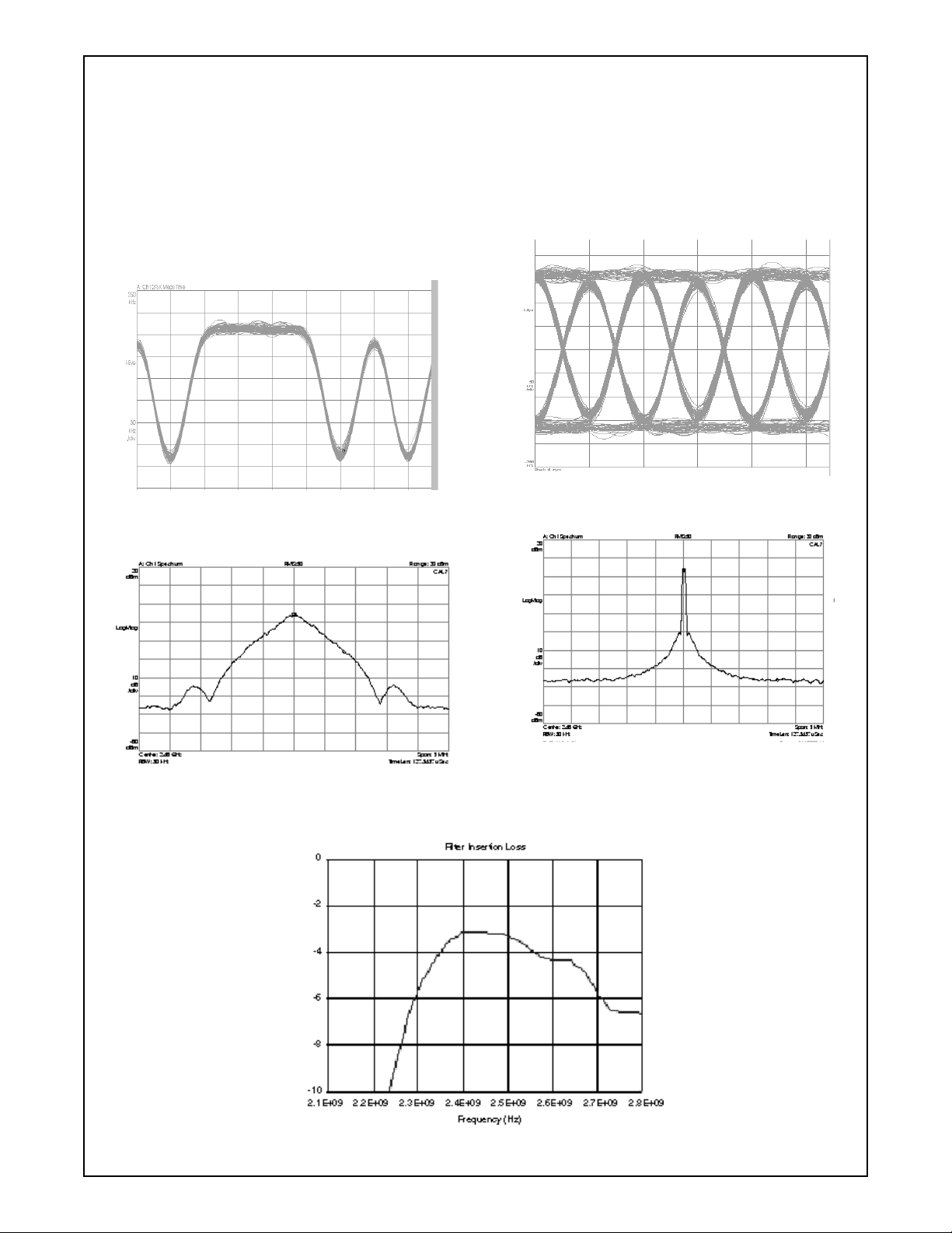
6.4 PERFORMANCE DATA (T YPICAL)
IL(dB)
LMX9820A Bluetooth Serial Port Module
Figure 5. Corresponding Eye Diagram
Figure 3. Modulation
Figure 6. Synthesizer Phase Noise
Figure 4. Transmit Spectrum
0
-2
-4
-6
-8
-10
Filter Insertion Loss
Frequency (Hz)
2.8E+0
2.7E+092.2E+092.1E+09 2.3E+09 2.4E+09 2.5E+09 2.6E+09
Figure 7. Front-End Bandpass Filter Response
www.nationa l.c om 12 R ev is io n 1.0

6.0 Electrical Specifications (Continued)
LMX9820A Bluetooth Serial Port Module
1.00
2.00
0.50
S(1.1)
m2
freq = 2.402 GHz
S(1.1) = 0.093/-29.733
impedance = Z0* (1.170 - j0.109)
m1
freq = 2.500 GHz
S(1.1) = 0.035/175.614
impedance = Z0* (0.933 + j0.005)
Figure 8. TX and RX Pin 50Ω Impedance Characteristics
0.00
-0.50
0.50
m1
1.00
freq(2.400 GHz to 2.500 GHz)
m2
-1.00
2.00
-2.00
Revision 1.0 13 www.national.com

7.0 Functional Description (Continued)
LMX9820A Bluetooth Serial Port Module
Figure 9. Transceiver Return Loss
7.0 Functional Description
7.1 BASEBAND AND LINK MANAGEMENT
PROCESSORS
Baseband and Lower Link control functions are implemented using a combination of National Semiconductor’s
CompactRISC 16-bit processor and the Bluetooth Lower
Link Controller. These processors operate from integrated
Flash memory and RAM and execute on-board firmware
implementing all Bl uetooth functions.
7.1.1 Bluetooth Lower Link Controller
The integrated Bluetooth Lower Link Controller (LLC) complies with the Bluetooth Specification version 1.1 and
implements the f oll owing functions:
• Support for 1, 3, and 5 slot packet types
• 79-channel hop frequency generation circuitry
• Fast frequency hopping at 1600 hops per second
• Power management control
• Access code corr elation and slot timing recovery
7.1.2 Bluetooth Upper Layer Stack
The integrated upper layer stack is prequalified and
includes the following protocol layers:
• L2CAP
• RFComm
• SDP
7.1.3 Profile Support
The on-chip applicati on of th e LMX982 0A all ows ful l standalone operation, without any Bluetooth protocol layer necessary outside the module. It supports the Generic Access
Profile (GAP), the Service Discovery Application Profile
(SDAP), and the Serial Port Profile (SPP) .
The on-chip prof il es can be used as inter faces to additional
profiles executed on the host. The LMX9820A includes a
configurable service database to answer requests with the
profiles suppo rted.
7.1.4 Application with Command Int erface
The module supports automatic slave operation eliminating
the need for an external control unit. The implemented
transparent option enables the chip to handle incoming
data raw, without the need for packaging in a special format. The device uses a fixed pin to block unallowed connections.
Acting as master, the application offers a simple but versatile command interface for standard Bluetooth operations
such as inquiry, service discovery, and serial port connection. The firmware supports up to three slaves. Default L ink
Policy settings and a specific master mode allow optimized
configuration for the application specific requirements. See
also Section "Integrated Firmware" on page 24.
www.nationa l.c om 14 R ev is io n 1.0

7.0 Functional Description (Continued)
LMX9820A Bluetooth Serial Port Module
7.2 MEMORY
The LMX9820A includes 256KB of programmable Flash
memory that can be used for code and constant data. It
allows single-cycle read access from the CPU. In addition
to storing all algorithms and firmware, the on-board Flash
also contains the IEEE 802 compliant Media Access Controller (MAC) address (BDADDR). The firmware and the
BDADDR are programmed by National Semiconductor or
can be programmed by the customer either before assembly into the host system or in-system. Module firmware can
also be updated during manufacturing or in-system using
the ISP capabilities of the LMX9820A. The LMX9820A
firmware uses the internal RAM for buffers and program
variables.
7.3 CONTROL AND TRANSPORT PORT
The LMX9820A provides one Universal Asynchronous
Receiver Transmitter (UART). It support s 8-bit data format s
with or without parity and one or two stop bits. The baud
rate is generated by hardware that is programmed at boot
time. Alternatively, the speed and configuration settings
can be read out of internal memory settings. The UART
can operate at baud rates of 2.4k, 4.8k, 7.2k, 9.6k, 19.2k,
38.4k, 57.6k, 115.2k, 230.4k, 460.8k and 921.6k. It imple-
ments flow control logic (RTS, CTS) to provide hardware
handshaking capability. The UART offers wakeup from the
low-power modes through the multi-input wakeup module.
UART logic thresholds are set via the IOVCC pin.
7.4 AUXILIARY PORTS
7.4.1 Reset_5100 and Reset_b#
Reset_5100 and Reset_b# are active low reset inputs for
the baseband controller and digital smart radio portions of
the LMX9820A, respectively. These pins are normally tied
together and are connected to the host system so that the
host can initialize the LMX9820A by asserting the reset
inputs. Upon de- assertion, the stat us of the module operating environment (Env) pads are sampled and the
LMX9820A enters the corr esponding operational mode.
7.4.2 Operating Environm ent Pads (Env0 and Env1)
The module provides two operating environments (see
Table 17) selected by the states on the Env inputs sampled
at reset.
The ISP mode allows end-of-line or field programming of
the LMX9820A Flash memory by starting the baseband
controller from the boot block of memory.
7.4.3 Interface Select Inputs (ISEL1, ISEL2)
The interface selection pads are used for setting the UART
speed and settings. If ISEL1 and ISEL2 are unconnected,
they are pulled high by weak internal pullups, which select
a default baudrate of 921.6k baud. The settings for Stopbits, Startbit, and Parity are stored as internal non-volatile
storage (NVS) parameters. If a baud rate different from the
values listed in Table 18 is needed, ISEL 1 and ISEL2 must
be pulled low. This forces the device to read the UART
speed from the parameter table in NVS. The default baud
rate value programmed in NVS is 9.6k baud, however the
device firmware can be modified to support other values.
The default configur ation i n NVS is 1 St opbit, 1 S t art bit, and
No parity. Table 18 shows the ISEL1 and ISEL2 selection
settings.
T able 18. UART Speed Selection
ISEL1
(Pad J13)
1 1 921.6k Fr om NV S
0 1 115.2k Fr om NV S
1 0 9.6k 1Stop, 1Start,
0 0 Check NVS From NVS
7.4.4 Module and LInk Status Outputs
The LMX9820A provides signals that the host can use to
determine the real-time status of the radio link. The
TX_Switch_P signal (pad H3) is a real-time indication of
the current configuration (direction) of the transceiver. The
link status lines (Lstat_0 and Lstat_1, pads E8 and F8,
respectively) are GPIO lines controlled by the LMX9820A
firmware. The Host Wakeup line (Host_wu, pad F9) is
implemented using GPIO and firmware. It is used to bring
the host processor out of Sleep mode when link activity
calls for host processing. Host_wu can also be used by the
host to check if link activity is present. If Host_wu is active,
then link activity is present and the host loses network
awareness if the operating system continues to allow the
host processor to enter Sleep mode. Table 19 presents the
definitions of t he various module and link status outputs.
T able 19. Module/Link Status Defini ti ons
ISEL2
(Pad H13)
Interface
Speed (baud)
UART
Settings
No Parity
T able 17. Operating Environments
Operating Environment
ISP Mode 1 0
Run (Normal) Mode (De-
fault)
Revision 1.0 15 www.national.com
Env1
(Pad B11)
11
Env0
(Pad E9)
Lstat_0
x 1 x x At least 1 SPP link es-
x 0 x x No active SPP link
x x 1 x Transceiver = Transmit
x x 0 x Transceiver = Receive
x x x 0 Host can Sleep
x x x 1 Wakeup host/host
Lstat_1
(Pad E8)
(Pad F8)
(Pad H3)
TX_Switch_P
(Pad F9)
Host_wu
tablished
should not Sleep
Mode

7.0 Functional Description (Continued)
7.5 AUDIO PORT
Advanced Audio Interface
The Advanced Audio Interface (AAI) is an advanced version of the Synchronous Serial Interface (SSI) that provides a full-duplex communications port to a variety of
industry-standard 13/14/15/16-bit linear or 8-bit log PCM
codecs, DSPs, and other serial audio devices.
T able 20. Audio Path Configurati on
Audio Path Format AAI Bit Clock AAI Frame Clock
Motorola MC145483
OKI MSM7717
1. Due to internal clock di vider limitation s, the optimum of 512 kHz, 8 kHz cannot be reached. The values are set to the
LMX9820A Bluetooth Serial Port Module
best possible values. The clock mismatch does not result in any discernible loss in audio qualit y.
1
13-bit linear 480 kHz 8 kHz 13 bits
8-bit log PCM
(A-law only)
The LMX9820A allows the support for one codec. The
firmware selects the desired audio path and interface configuration by a parameter stored in NVS. The audio path
options include the Motorola MC145483 codec, the OKI
MSM7717 codec through the AAI, or no audio.
Table 20 summari zes the audio path se lection and the configuration of the audio interface at the specific mode.
AAI Frame Sync
Pulse Length
120 kHz 8 kHz 14 bits
www.nationa l.c om 16 R ev is io n 1.0

8.0 Digital Smart Radio (Continued)
LMX9820A Bluetooth Serial Port Module
8.0 Digital Smart Radio
8.1 FUNCTIONAL DESCRIPTION
The integrated Digital Smart Radio uses a heterodyne receiver architecture with a low intermediate frequency (2
MHz), such that t he int ermedi ate frequ ency filte rs can be i ntegrated on-chip. The receiver consists of a low-noise amplifier (LNA) followed by two mixers. The intermediate
frequency signal processing blocks consist of a poly-phase
bandpass filter (BPF), two hard limiters (LIM), a frequency
discriminator (DET), and a post-detection filter (PDF). The
received signal level is detected by a received signal
strength indicator (RSSI).
The received frequency equals the local oscillator frequency (fLO) plus the inter m ediate frequency (fIF) :
fRF = fLO + fIF (supradyne).
The radio includes a synthesizer consisting of a phase de-
tector, a charge pump, an (off-chip) loop filter, an RF frequency divider, and a voltage- controlled oscillator (VCO).
The transmitter uses IQ-modulation with bit-stream data
that is gaussian filtered. Other blocks included in the transmitter are a VCO buffer and a power ampli fier (PA).
8.2 RECEIVER FRONT END
The receiver front end consists of a low-noise amplifier
(LNA) followed by t wo mixers an d two low-p ass fil ters for th e
I- and Q-channels.
The intermediate frequency (IF) part of the receiver front
end consists of two IF amplifiers that receive input signals
from the mixers, delivering balanced I- and Q-signals to the
poly-phase bandpass filter. The poly-phase bandpass filter
is directly followed by two hard limiters that together generate an AD-converted RSSI signal.
8.2.1 Poly-Phase Bandpass Filt er
The purpose of the IF bandpass filter is to reject noise and
spurious (mainly adjacent channel) interference that would
otherwise enter the hard-limiting stage. In addition, it handles image reject ion.
The bandpass f il ter uses both the I- and Q-signals from the
mixers. The out-of-band suppression should be higher than
40 dB (f < 1 MHz, f > 3 MHz). The bandpass filter is tuned
over process spread and temperature variations by the autotuner circuitry. A 5th-order Butterworth filter is used.
8.2.2 Hard Limiter and RSSI
The I- and Q-outputs of the bandpass filter are each followed by a hard-limiter. The hard-limiter has its own reference current. The RSSI (Received Signal Strength
Indicator) repor ts the level of the RF input signal .
The RSSI is generated by piece-wise linear approximation
of the level of the RF signal. The RSSI has a mV/dB scale,
and an analog-to-digital converter for processing by the
baseband circui t. T he input RF po wer is convert ed to a 5-bit
value. The RSSI value i s then pr opor tion al to the i nput power (in dBm).
The digital output from the ADC is sampled on the BPKTCTL signal low-to-high tr ansition.
8.3 RECEIVER BACK END
The hard limiters are followed by two frequenc y discriminators. The I-frequency discriminator uses the 90
shifted signal from the Q-path, while the Q-discriminator
uses the 90
phase bandpass filter performs the required phase shifting.
The output signals of the I- and Q-discriminator are subtracted and filtered by a low-pass filter. An equalizer is added to improve the eye-p attern for 101010 patterns.
After equalizat ion, a dynamic AFC (automatic frequ ency offset compensation) circuit and slicer extract the RX_DATA
from the analog data patt ern. The Eb/No of the demodulat or
is approximately 17 dB.
8.3.1 Frequency Discri minator
The frequency discriminator gets its input signals from the
limiter. A defined signal level (independent of the power
supply volt age) i s needed t o obt ain the inp ut sig nal. Bot h inputs of the frequency discriminator have limiting circuits to
optimize performance. The bandpass filter in the frequency
discriminator is tuned by the autotuning circuitry.
8.3.2 Post-Detection Fi lt er and Equalizer
The output signals of the FM discriminator go through a
post-detection filter followed by an equalizer. Bo th the postdetection filter and equalizer are tuned to the proper frequency by the autotuning circuitry. The post-detection filter
is a low-p ass filter int ended to suppress all remaining spurious signals, suc h as the second harmoni c (4 MHz ) from the
FM detector and noise generated after the limiter.
The post-detection filter also helps for attenuating the first
adjacent channel signal. The equalizer improves the eyeopening for 101010 patterns. The post-detection filter is a
third-order Butterworth filter.
o
phase-shifted signal from the I-path. A poly-
o
phase-
8.4 AUTOTUNING CIRCUITRY
The autotuning circuitry is used for tuning the bandpass filter, detector , post-detection filter , equalizer, and transm it filters for process and temperature variations. The circuitry
includes offset compensation for the FM detector.
8.5 SYNTHESIZER
The synthesizer consists of a phase-frequency detector, a
charge pump, a low-pass loop filter, a programmable frequency divider, a voltage-controlled osci ll ator (VCO), a delta-sigma modulator, and a lookup table.
The frequency divider consists of a divide-by-2 circuit (divides the 5 GHz signal from the VCO down to 2.5 GHz), a
divide-by-8-or-9 divider, and a digital modulus control. The
delta-sigma modulator controls the division ratio and also
generates an input channel value to the lookup table.
8.5.1 Phase-Frequency Det ector
The phase-frequency detector is a 5-state phase-detector.
It responds only to transitions, hence phase-error is inde-
Revision 1.0 17 www.national.com

8.0 Digital Smart Radio (Continued)
pendent of input waveform duty cycle or amplitude variations. Loop lockup occurs when all the negative transitions
on the inputs, F_REF and F_MOD, coincide. Both outputs
(i.e., Up and Down) then remain high. This is equal to the
zero error mode. The phase-frequency detector input frequency range operates at 12 MHz.
8.6 TRANSMITTER CIRCUITRY
The transmitter consists of ROM tables, two Digital to Analog (DA) converters, two low-pass filters, IQ mixers, and a
power amplifier (PA).
The ROM tables generate a digital IQ signal based on the
transmit dat a. The output of the ROM tables is insert ed into
IQ-DA converters and filtered through two low-pass filters.
The two signal component s are mixed up to 2.5 GHz by the
TX mixers and added together before being inserted into
the trans m it PA.
LMX9820A Bluetooth Serial Port Module
8.6.1 IQ-DA Converters and TX Mixers
The ROM output signals drive an I- and Q-DA converter.
Two But terwor th low-p ass f ilter s fil ter t he DA output signal s.
The 6 MHz clock for the DA converter s and the logi c circ uitry around the ROM tables are derived from the autotuner.
The TX mixers mix the balanced I- and Q -signals up to 2.4-
2.5 GHz. The output signals of the I- and Q-mixers are
summed.
8.7 CRYSTAL REQUIREMENTS
The LMX9820A includes a crystal driver circuit. This circuit
operates with an external crystal and capacitors to form an
oscillator. Figure 10 shows the recommended crystal ci rcuit.
Table 24 on page 22 specifies system clock req uir em ents.
The RF local oscillator and internal digital clocks for the
LMX9820A are derived from the reference clock at the
CLK+ input. This reference may either come from an external clock or a dedicated crystal oscillator. The crystal oscillator connections require a crystal and two grounded
capacitors.
onant frequency may be trimmed with the crystal load
capacitance.
1. Load Capacit ance
For resonance at the correct frequency, the crystal should
be loaded with its specified load capacitance, which is the
value of capacitance used in conjunction with the crystal
unit. Load capacitance is a parameter specified by the
crystal, typically expressed in pF. The crystal circuit shown
in Figure 11 on page 19 is composed of:
— C1 (motional capacitance)
— R1 (motional resistance)
— L1 (motional inductance)
— C0 (static or shunt capacitance)
The LMX9820A provides some of the load with internal
capacitors C
nal capacitors and tuning capacitors labeled Ct1 and Ct2
. The remainder must come from the exter-
int
as shown in Figure 10. Ct1 and Ct2 should have the same
the value for best noise performance.
The LMX9820A has an additional internal capacitance
C
of 2.6 pF. Crystal load capacitance (CL) is calculated
TUNE
as:
C
= C
+ C
L
int
The C
capacitance C
above does not include the crystal internal self-
L
total capacitance is:
C
= CL + C
total
+ Ct1/Ct2
TUNE
as shown in Figure 11 on page 19, so the
0
0
Based on the crystal specification and equati on:
= C
C
C
+ C
L
int
= 8pF + 2.6pF + 6pF = 16.6pF
L
TUNE
+ Ct1//Ct2
16.6 pF is very close to the TEW crystal requirement of 16
pF load capacitance. With the internal shunt capacitance
C
:
total
= 16.6pF + 5pF = 21.6pF
C
total
LMX9820A
CLK+ CLK-
C
int
It is important to consider board- and design-dependent
capacitance in tuning the crystal circuit. The following
C
TUNE
equations allow a close approximation of th e required crystal tuning capacitance, but the actual values will vary with
the capacitive properties of the board. As a result, there is
some fine tuning of the crystal circuit which cannot be calculated, but must be determined experimentally by testing
differen t val ues of load capacit ance.
Many different crystals can be used with the LMX9820A. A
Ct1
Crystal
Ct2
key requirement from the Bluetooth specification is 20
ppm. Additionally, ESR (Equivalent Series Resistance)
must be carefully considered. LMX9820A can support a
maximum of 230Ω ESR, but it is recommended to stay <
100Ω ESR for best performance over v oltage and temper a-
Figure 10. LMX9820A Crystal Recommended
Circuit
ture. See Figure 14 on page 22 for ESR as part of the crystal circu it fo r more in fo rmation .
8.7.1 Crystal
The crystal appears inductive near its resonant frequency.
It forms a resonant circuit with its load capacitors. The res-
www.nationa l.c om 18 R ev is io n 1.0

8.0 Digital Smart Radio (Continued)
LMX9820A Bluetooth Serial Port Module
R1 C1 L1
C0
Figure 11. Crystal Equivalent Circuit
2. Crystal Pullability
Pullability is another important parameter for a crystal,
which is the change in frequency of a crystal with units of
ppm/pF, either from the natural resonant frequency to a
load resonant frequency or from one load resonant frequency to another. The frequency can be pulled in a parallel resonant circuit by changing the value of load
capacitance. A decrease in load capacitance causes an
increase in frequency, and an increase in load capacitance
causes a decrease in fr equency .
3. Frequency Tuning
Frequency tuning is achieved by adjusting the crystal load
capacitance with external capacitors. It is a Bluetooth
requirement that the frequency is always within 20 ppm.
The crystal network or oscillator must have cumulative
accuracy specifications of 15 ppm to provide margin for
frequency drift wi th agi ng and temperature.
Revision 1.0 19 www.national.com

8.0 Digital Smart Radio (Continued)
TEW Crystal
The LMX9820A has been tested with the TEW TAS-4025A
crystal, see Table 21 on page 20 for specification.
Because the internal capacitance of the crystal circuit is 8
pF and the load capacitanc e is 16 pF, 12 pF is a good starting point for both Ct1 and Ct2. The 2480 MHz RF frequency offset is then tested. Figure 12 on page 21 shows
the RF frequency of fset test results.
Figure 12 on page 21 shows the results are -20 kHz off the
center frequency, which is -1 ppm. The pullability of the
crystal is 2 ppm/pF, so the load capacitance must be
decreased by about 1.0 pF. By changing Ct1 or Ct2 to
10 pF, the total load capacitance is decreased by 1.0 pF.
Figure 13 on page 21 shows the frequency offset test
resuts. The frequency offset is now zero with Ct1 = 10 pF,
Ct2 = 10 pF.
Reference Table 22 on page 20 for crystal tuning values
used on Austin Development Board with TEW crystal.
LMX9820A Bluetooth Serial Port Module
T able 21. TEW TAS-4025A
Specification Value
Package 4.0 x 2.5 x 0.65 mm (4 pads)
Frequency 12.000 MHz
Mode Fundamental
St ability >15 ppm @ -40 to +85°C
C
Load Capacitance 16 pF
L
ESR 80Ω max.
C
Shunt Capacitanc e 5 pF
0
Drive Level 50 ±10uV
Pullabilit y 2 ppm/pF min
St orage Temperature -40 to +85°C
Table 22. TEW on Arizona Board
Reference LMX9820A
Ct1 10 pF
Ct2 10 pF
www.nationa l.c om 20 R ev is io n 1.0

8.0 Digital Smart Radio (Continued)
Figure 12. Frequency Offset with 12 pF/12 pF Capacitors
LMX9820A Bluetooth Serial Port Module
Figure 13. Frequency Offset with 10 pF/10 pF Capacitors
8.7.2 TCXO (Temperature Compensated Crystal
Oscillator)
The LMX9820A also can operate with an external TCXO
(Temperature Compensated Crystal Oscillator). The TCXO
signal is direct ly connected to the CLK+, shown in Table 23
on page 21.
1. Input Imp edance
The LMX9820A CLK+ pin has in input impedance of 2 pF
capacitance in parallel with >400kΩ resistance.
2. NKG3184A TCXO
The LMX9820A has also been tested with the NKG3184A
TCXO. See Table 23 on page 21.
T able 23. TCXO NKG3184A
Specification Value
Package 5.0 x 3.2 x 1.4 mm (4 pads)
Frequency 12.000 MHz
Stability 18 ppm at -30 to +85°C
(inclusive of all conditions)
Output Load 10kΩ/13 pF
Current Consumption 2.0 mA
Output Level 0.3Vp-p to 2.0Vp-p
Storage Temperature -40 to +85°C
DC Cut Capacitor Included in VC-TCXO
Revision 1.0 21 www.national.com

8.0 Digital Smart Radio (Continued)
8.7.3 ESR (Equivalent Series Resistance)
LMX9820A can operate with a wide range of crystals with
different ESR ratings. Reference Table 24 on page 22 and
Figure 14 on page 22 for more details.
Ta ble 24. System Clock Requireme nts
Parameter Min Typ Max Unit
External Reference Clock Frequency 12 MHz MHz
Frequency Tolerance (over full operating temperature and aging) 15 20 ppm
Crystal Serial Resistanc e 230 Ω
External Reference Clock Power Swing, pk to pk 100 200 400 mV
Aging 1ppm
LMX9820A Bluetooth Serial Port Module
per
year
Figure 14. ESR vs. Load Capacitance for the Crystal
www.nationa l.c om 22 R ev is io n 1.0

9.0 System Power-Up Sequence (Continued)
LMX9820A Bluetooth Serial Port Module
9.0 System Power-Up Sequence
The following sequence must be performed to correctly
power-up the LMX9820A:
1. Apply IOVCC and VCC to the LMX9820A.
VCC
IOVCC
Reset_b#
Reset_5100
BBP_CLOCK
TX_RX_DATA
TX_RX_SYNC
CCB_DATA
CCB_CLOCK
Low
t
PTOR
Low
High
Low
Low
Low
2. Reset_b# and Reset_5100# of the LMX9820A are d riven
high a minimum of 2 ms after the LMX9820A voltage
rails are high. The LMX9820A i s the properly reset.
See Table 25 on page 23.
CCB_LATCH
High
LMX9820A
Oscillator
Start-Up
Power-Up Mode
LMX9820A in
LMX9820A
Initialization
Standby Active
LMX9820A
Initialization
LMX9820A in Normal Mode
Figure 15. LMX9820A System Power-Up Sequence Timing
Table 25. LMX9820A System Power-up Sequence Timing
Symbol Parameter Condition Min Typ Max Unit
t
PTOR
Power to Reset VCC and IO
at operating
VCC
2ms
voltage le ve l to va li d res e t
Revision 1.0 23 www.national.com

10.0 Integrated Firmware (Continued)
10.0 Integrated Firmwar e
The LMX9820A includes the full Bluetooth protocol stack
up to RFComm to support the following profiles:
— GAP (Generic Access Profile)
— SDAP (Service Discovery Application Profile)
— SPP (Serial Port Profile)
Figure 16 shows the Bluetooth protocol stack with com-
mand interpreter interface. The command interpreter offers
a number of different commands to support the functionality given by the different profiles. Execution and interface
timing is handled by the control application.
The chip has an internal data area in Flash that includes
the parameters shown in Table 26 on page 25.
LMX9820A Bluetooth Serial Port Module
Command Interpreter
Control Application
SPP
RFComm
L2CAP
Link Manager
Baseband
Figure 16. LMX9820A Software Implementation
10.1 FEATURES
10.1.1 Operation Modes
On boot-up, the application configures the module following the parameter s in the data area.
Automatic Mode
No Default Connections Stor ed
In Automatic mode the module is connectable and discoverable and automatically answers to service requests. The
command interpreter listens to commands and links can be
set up. The full command list is supported.
If connected by another device, the module sends an event
back to the host, where the RFComm port has been connected, and switch es to t ransparent mode.
Default Connections Stored
If default connections were stored on a previous session,
after th e LM X982 0A is res et, it w ill at temp t to reconnect to
each device stored within the data Flash three times. The
host will be notified about the success of the link setup via
a link status event.
Command Mode
In Command mode, the LMX9820A does not check the
default connections section within the Data Flash. If con-
SDAP
GAP
SDP
nected by another device, it will not switch to transparent
mode and continue to interpret data sent on the UART.
Transparent Mode
The LMX9820A supports transparent data communication
from the UART interface to a Bluetooth link.
If activated, the module does not interpret the commands
on the UART which normally are used to configure and
control the module. In this case, the packets do not need to
be formatted as described in Table 28 on page 27. Instead,
all data are directly passed through the firmware to the
active Bluetooth link and the remote device.
Transparent mode can only be supported on a point-topoint connection. To leave Transparent mode, the host
must send a UART_BREAK signal to the mod ule
Force Master Mode
In Force Master mode, the LMX9820A tries to act like an
Access point for multiple connections. In this mode, it will
only accept a link if a master/slave role switch is accepted
by the connecting device. After successful link establishment, the LMX9820A will be master and available for additional incoming links. On the first incoming link the
LMX9820A may switch to transparent mode, depending on
the setting for automatic or command mode. Additional
links will o nly be p ossib le if the d evice is not in tran spare nt
mode.
10.1.2 Default Connections
The LMX9820A supports the st orage of up to 3 default connections within its NVS. Those connections can either be
connected after reset or on demand using a specific command.
10.1.3 Event Filter
The LMX9820A uses events or indicators to notify the host
about successful commands or changes on the Bluetooth
interface. Depending on the application, the LMX9820A
can be configured. The fol lowing levels are define d:
• No Events—the LMX9820A is not reporting any eve nts.
Optimized for pas sive cable replacement solutions.
• Standard LMX9820A Events—only necessary events
will be reported.
• All Events—additional to the st andard all changes at the
physical layer wil l be r eported.
10.1.4 Default Link Policy
Each Bluetooth link can be configured to support master/slave role switch, Hold mode, Sniff mode, and Park
mode. The default link policy defines the standard setting
for incoming and outgoing connections.
10.1.5 Audio Support
The LMX9820A offers commands to establish and release
synchronous connections (SCO) to support Headset or
Handsfree applications. The firmware supports one active
link with all available package types (HV1, HV2, HV3), for
routing audio data between the Bluetooth link and the
advanced audio interface. To provide the analog data interface, an external audio codec is required. The LMX9820A
includes a list of codecs which can be used.
www.nationa l.c om 24 R ev is io n 1.0

10.0 Integrated Firmware (Continued)
T able 26. Operation Param eters Stored in LMX9820A
Parameter Default Value Description
BDADDR (Hardcoded into device) Bluetooth device address
Local Name Serial port device
PinCode 0000 Bluetooth PinCode
Operation Mode Automatic Command or Automatic mode
Default Connections 0 Up to three default devi ces to connect on default
SDP Database 1 SPP entry:
UART Speed 9600 Sets the s peed of the physica l UART in terfa ce to t he
UART Settings 1 Stop bit, parity disabled Par ity and stop bits on the hardware UART interface
Ports to Open 0000 0001 Defines the RFComm ports to open
Link Keys No link keys Link keys for paired devices
Security Mode 2 Security mode
Page Scan Mode Connectable Connectable/Not connectable for othe r devi ces
Inquiry Scan Mode Discoverable Discoverable/Not Discove rable/Limited Discoverable
Default Link Policy All modes allowed Configures modes allowed for incoming or outgoin g
Default Link Timeout 20 seconds The Default Link Timeout configures the timeout, af-
Event Filter Standard LMX9820A events reported Defines the level of reporting on the UART
Default Audio Settings
Name: COM1
Authentication and encryption enabled
None Configures the settings for the external codec and
Service disco very database, control for supported
profiles
host
for other devices
connections (master/slave role switch, Hold mode,
Sniff mode, Park mode)
ter which the link i s assume d lost, if no packages
have been received from the remote device.
- No event s
- Standard events
- Standard including ACL link events
the air interfa ce for m at.
• Codecs:
— Motorola MC145483
— OKI MSM7717
LMX9820A Bluetooth Serial Port Module
• Air format:
— CVSD
— µ-Law
—A-Law
Revision 1.0 25 www.national.com

11.0 Power Reduction (Continued)
11.0 Power Reduction
The LMX9820A supports several low-power modes to
reduce power in di fferent operati ng situations. The modular
structure of the LMX9820A allows the firmware to power
down unused modules.
The low-power modes have influence on:
• UART transport l ayer—enables or disables the in ter-
face.
• Bluetooth Baseband activity—firmware disables LLC
and radio, if possible.
11.1 LOW POWER MODES
The following LMX9820A power modes, which depend on
the activity level of the UART transport layer and the radio
activity, are defined:
LMX9820A Bluetooth Serial Port Module
The activity of the Bluetoot h radio mainly depen ds on application requirements and is controlled by standard Bluetooth operations such as inquiry/page scanning or an
active link. A r em ote device establishing or disconnecting a
link may also indirectly change the activity level of the
radio.
The UART transport layer by default is enabled on device
power up. The “Disable Transport Layer” command is used
to disable the transport layer. Therefore, only the host-side
command interface can disable the transport layer.
Enabling the transport layer is controlled by the hardware
wake-up signalling. This can be initiated from either the
host or an LMX9820A input. See also “LMX9820A Software Users Guide” for detailed information on timing and
implementati on requirements.
Table 27. Power Mode Activity
Power
Mode
UART
Bluetooth
Radio
Reference
PM0 Off Off None
PM1 On Off 12 MHz
PM2 Off Scanning 12 MHz
PM3 On Scanni ng 12 MHz
PM4 Off SPP Link 12 MHz
PM5 On SPP Link 12 MHz
11.2 UART TRANSPORT LA YER CONTROL
11.2.1 Hardware Wake-Up Functionalit y
In some circumstances, the host may switch off the transport layer of the LMX9820A to reduce power consumption.
The host and LMX9820A then may shut down their UART
interfaces.
To simplify the system design, the UART interface is configured for hardware wake-up functionality. For a detailed
timing and command functionality, see the “LMX9820A
Software Users Gui de”.
The interface between the host and LMX9820A i s shown in
Figure 17.
Clock
LMX9820A
RTS#
CTS#
TX
RX
Host_WU
RTS#
CTS#
TX
RX
GPIO
(optional)
Host
Figure 17. UART Null Modem Connections
11.2.2 Disabling the UART Transport Layer
The host can disable the UART transport layer by sending
the “Disable Transport Layer” Command. The LMX9820A
will empty its buffers, send the confirmation event, and disable its UART interface. The UART interface will then be
reconfigured to wake up the LMX9820A on a falling edge of
the CTS pin.
11.2.3 LMX9820A Enabling the UART Interface
Because the transport layer can be disabled in any situation, the LMX9820A must verify that the transport layer is
enabled before sending data to the host. Possible situations in which the LMX9820A will need to re-enable the
interface include incoming data or incoming link indicators.
If the UART is not enabled, the LMX9820A must assume
that the host is in a low-power mode and initiate a wake-up
event by asserting RTS and setting HOST_WU to 1. To be
able to respond to the wake-up event, the host must monitor its CTS input (i.e. the LMX9820A RTS output).
As soon as the host activates its RTS output (i.e. the
LMX9820A CTS inpu t) , the LMX9820A wil l first send a c onfirmation even t and th en start to transmit the events.
11.2.4 Enabling the UART Transport Layer fr om Host
If the host needs to send data or commands to the
LMX9820A while the UART transport layer is disabled, it
must first assume that the LMX9820A is sleeping and wake
it up by asserting the host RTS output (i.e. the LMX9820A
CTS input).
When the LMX9820A detects the wake-up signal, it
enables the UART and acknowledges the wake-up signal
by asserting its RTS output and HOST_WU signal. Additionally, the wake-up event will be acknowledged by sending a confirmation event. When the host has received this
“Transport Layer Enabled” event, it knows the LMX9820A
is ready to receive commands.
www.nationa l.c om 26 R ev is io n 1.0

12.0 Command Interface (Continued)
LMX9820A Bluetooth Serial Port Module
12.0 Command Interfac e
The LMX9820A offers Bluetooth functionality through
either a self-contained slave functionality or a simple command interface. The interface is carried over the UART
interface.
The following sections describe the protocol on the UART
interface between the LMX9820A and the host in command mode (see Figure 18). In Transparent mode, no data
framing is necessary and the device does not interpret data
carried over the interface as commands.
12.1 FR AMING
The connection is considered “Error free”. But for packet
recognition and synchronization, some framing is used.
All packet s sent in both directions are constructed followin g
the model shown in Table 28.
12.1.1 Start and End Delimiters
The “STX” character is used as the start delimiter: STX =
0x02. ETX = 0x03 is used as the end delimiter.
LMX9820A
12.1.2 Packet Type ID
This byte identifies the type of packet. See Table 29 for
details.
12.1.3 Opcode
The opcode identifies the command to execute. The
opcode values can be found within the “LMX9820A Software User’s Guide” included with the LMX9820A Evaluation Board.
12.1.4 Data Length
Number of bytes in the Packet Data field. The maximum
size is 333 data byt es per packet.
12.1.5 Checksum
This is a simple Block Check Character (BCC) checksum
of the bytes “Packet type”, “Opcode”, and “Data Length”.
The BCC checksum is calculated as low byte of the sum of
all bytes (e.g., if the sum of all bytes is 0x3724, the checksum is 0x24).
Existing device
without Bluetooth™
capabilities
UART
UART
Figure 18. Bluetooth Functionality
.
Table 28. Packet Framing
Start
Delimiter
Packet
Type ID
Opcode Data Length Checksum Packet Data
1 Byte 1 Byte 1 Byte 2 Bytes 1 Byte <Data Length> Bytes 1 Byte
- - - - - - - - - - - - - Checksum - - - - - - - - - - - - -
T able 29. Packet Type Identi fi cation
ID Direction Description
0x52
‘R’
0x43
‘C’
0x69
‘i’
0x72
‘r’
REQUEST
(REQ)
Confirm
(CFM)
Indication
(IND)
Response
(RES)
A request sent to the Blueto oth module.
All requests are answered by exactly one confirm.
The Bluetooth modules confirm to a request.
All requests are answered by exactly one confirm.
Information sent from the Bluetooth module that is not a direct confirm to a request.
Indicating status changes, incoming links, or unrequested events.
An optional response to an in dication.
This is used to respond to some type of indication message.
End
Delimiter
Revision 1.0 27 www.national.com

12.0 Command Interface (Continued)
12.2 COMMAND SET OVERVIEW
The LMX9820A has a well-defined command set to:
• Configure the devi ce:
– Hardware settin gs
– Local Bluetooth parameters
– Service database
• Set up and handle links
T able 30. Device Discovery Commands
Command Event Description
Inquiry Inquiry Complete Search for devices
Device Found Lists BDADDR and class of device
Remote Device Name Remote Device Name Confirm Get name of remote device
Tables 30 through 40 show the actual command set and
the events coming back from the device. A fully documented description of the commands can be found in the
“LMX9820A Software Users G uide”.
Note: For standard Bluetooth operation, only commands
from Table 30 through Table 32 are used. Most of the
remaining commands are onl y for configuration pur poses.
LMX9820A Bluetooth Serial Port Module
Ta ble 31. SDAP Client Commands
Command Event Description
SDAP Connect SDAP Connect Confirm Create an SDP connection to remote device
SDAP Disconnect SDAP Disconnect Confirm Disco nnect an active SDAP link
Connection Lost Notification for lost SDAP link
SDAP Service Browse Service Browse Confirm Get the services of the remote device
SDAP Service Search SDAP Service Search Confirm Search a specific ser vice on a remote device
SDAP Attribute Request SDAP Attribute Request Confirm Searches for services with specific attributes
Table 32. SPP Link Commands
Command Event Description
Establish SPP Link Establishing SPP Link Confirm Initiates link establ ishment to a remote device
Link Established Link successfu ll y established
Incoming Link A remote device established a link to the local
device
Set Link Timeout Set Link Timeout Confirm Confirms the supervision tim eout for the ex-
Get Link Timeout Get Link Timeout Confirm Get the supervision timeout for the existing
Release SPP Link Release SPP Link Confirm Initiate release of SPP link
SPP Send Data SPP Send Data Confirm Send data to specific SPP port
Incoming Data Incoming data from remote device
Transparent Mode Transparent Mode Confirm Switch to transparent mode on the UART
T able 33. Default Connection Commands
Command Event Description
Connect Default Connecti on Connect Default Connection Confi rm Connects to either one or all st ored default
Store Default Connection Store Default Connection Confirm Store device as default connection
Get List of Default Connections
Delete Default Connect ions Delete Default Connections Confirm
List of Default Devices
isting link
link
connections
www.nationa l.c om 28 R ev is io n 1.0

12.0 Command Interface (Continued)
T able 34. Power Mode Commands
Command Event Description
Set Default Link Policy Set Default Link Policy Confirm Defines the link policy used for any incoming
or outgoing link.
Get Default Link Polic y Get Default Link Policy Confirm Returns the stored default link policy
Set Link Policy Set Link Pol icy Confirm Defines the modes allowed for a specifi c li nk
Get Link Policy Get Link Policy Confirm Returns the actual link poli cy for the link
Enter Sniff Mode Enter Sniff Mode Confirm
Exit Sniff Mode Exit Sniff Mode Confirm
Enter Park Mode Enter Park Mode Confirm
Enter Hold Mode Enter Hold Mode Confirm
Power Save Mode Changed Remote device changed the power save
mode on the link
Table 35. Audio Control Commands
Command Event Description
Establish SCO Link Establish SCO Link Confirm Establish SCO link on existing RFComm
link
Release SCO Link Release SCO Link Confirm Release SCO link
SCO Link Established Indicator A remote device has established a SCO
link to the local device
SCO Link Released Indicator SCO link has been released
Change SCO Packet Type Change SCO Packet Type Confirm Changes packet type for existing SCO link
SCO Packet Type changed indicator SCO packet type has been changed
Set Audio Settings Set Audio Settings Confi rm Set audio settings for existing lin k
Get Audio Settings Get Audio Settings Confirm Get audio setting s for existing link
Set Volume Set Volume Confirm Configure the volume
Get Volume Get Volume Confirm Get current volume setting
Mute Mute Confi rm Mutes the microphone input
LMX9820A Bluetooth Serial Port Module
T able 36. Wake Up Function Commands
Command Event Description
Disable Transport Layer Transport Layer Enabled Disabling the UART transport la yer and
Revision 1.0 29 www.national.com
activates the hardware wake-up function

12.0 Command Interface (Continued)
T able 37. SPP Port Configuration and Status Commands
Command Event Description
Set Port Config Set Port Config Confirm Set port setting for th e “virtua l” ser ial po rt link
over the air
Get Port Config Get Port Config Confirm Read the actual port settings for a “virtual”
Port Config Changed Notification if port settings were changed
SPP Get Port Status SPP Get Port Status Confi rm Retur ns status of DTR and RTS (for the ac-
SPP Port Set DTR SPP Port Set DTR Confirm Sets the DTR bit on the specified link
SPP Port Set RTS SPP Port Set RTS Confirm Sets the RTS bit on the specified link
LMX9820A Bluetooth Serial Port Module
SPP Port BREAK SPP Port BREAK Indicates that the host has detected a break
SPP Port Overrun Error SPP Port Overrun Error Confirm Used to indicate that the host has detect ed an
SPP Port Parity Error SPP Port Parity Error Confirm Host has detected a parity error
SPP Port Framing Error SPP Port Framing Error Confirm Host has detected a framing err or
SPP Port Status Changed Indicates that remote device has changed
serial port
from remote device
tive RFComm link)
overrun error
one of the port status bi ts
T able 38. Local Settings Commands
Command Event Description
Read Local Name Read Local Name Confirm Read user-f ri endly name of the device
Write Local Name Write Local Name Confirm Set the user-friendly name of the device
Read Local BDADDR Read Local BDADDR Confirm
Change Local BDADDR Change Local BDADDR Confirm Note: Only use if you have your own
BDADDR pool
Store Class of Device Store Class of Device Confirm
Set Scan Mode Set Scan Mode Confirm Change mode for discoverability and
Set Scan Mode Indication Reports end of automatic limited
Get Fixed Pin Get Fixed Pin Confirm Reads current PinCode stored within the
Set Fixed Pin Set Fixed Pin Confirm Set the local PinCode
Get Security Mode Get Security Mode Confirm Get actual Security mode
Set Security Mode Set Security Mode Confirm Configure Security mode for local device
Remove Pairing Remove Pai ri ng Confirm Remove pairing with a remote device
List Paired Devices List of Paired Devices Get list of paired devices stored in the
Set Default Link Timeout Set Default Link Timeout Confirm Store default link supervision timeout
Get Default Link Timeout Get Default Link Ti me out Confirm Get stored defaul t link supervision timeout
Force Master Role Force Master Role Confirm Enables/Disables the request for master role
connectability
discoverabl e mo de
device
(default 2)
LMX9820A data memory
at incoming connec tions
www.nationa l.c om 30 R ev is io n 1.0

12.0 Command Interface (Continued)
T able 39. Local Service Database Configurat ion Comma nds
Command Event Description
Store SPP Record Store SPP Record Confirm Create a new SPP record within the service
database
Store DUN Record Store DUN Record Confirm Create a new DUN record within the service
database
Store FAX Record Store FAX Record Confirm Create a new FAX record within the service
database
Store OPP Record Store OPP Record Confirm Create a new OPP record within the service
database
Store FTP Record Store FTP Record Confirm Create a new FTP recor d wit hin the service
database
Store IrMCSync Record Store IrMCSync Record Confi rm Creat e a new IrMCSync record within the ser-
vice database
Enable SDP Record Enable SDP Record Confirm Enable or disable SDP records
Delete All SDP Records Delete All SDP Records Confir m
Ports to Open Ports to Open Confirmed Specify the RFCom m Ports to open on
startup
LMX9820A Bluetooth Serial Port Module
Table 40. Local Hardware Commands
Command Event Description
Set Default Audio Settings Set Default Audio Settings Confirm Configure default settings for audio codec
Get Default Audio Settings Get Default Audio Settings Confirm Get stored default audio settings
Set Event Filter Set Event Filter Confirm Configures the reporti ng level of the
Get Event Filter Get Event Filter Confirm Get the status of the reporting level
Read RSSI Read RSSI Confirm Returns an indicator for the incoming signal
Change UART Speed Change UART Speed Confirm Set specific UART speed; needs proper ISEL
Change UART Settings Change UART Sett ings Confirm Change configurati on for parity and stop bits
Test Mode Test Mode Confirm Enable Bluetooth, EMI test, or local loopback
Restore Factory Setti ngs Restore Factory Settings Confirm
Reset Dongle Ready Soft reset
Firmware Upgrade Stops the Bluetoo th f ir m wa re and executes
and air format, stored in NVS
command interface
strength
pin setting
the in-system programming code
Revision 1.0 31 www.national.com

13.0 Usage Scenarios (Continued)
13.0 Usage Scenarios
13.1 SCENARIO 1: POINT-TO-POINT CONNECTION
LMX9820A acts only as slave, no further configuration is
required.
Example: Sensor with LMX9820A; hand-held device with
standard Bluetooth option.
Sensor Device
UART
LMX9820A Bluetooth Serial Port Module
Inquiry Request
Inquiry Response
SDP Link Request
SDP Link Accept
Service Browse
Service Response
The SPP conformance of the LMX9820A allows any device
using the SPP to connect to the LMX9820A.
By switching to transparent mode automatically, the controller has no need for an additional protocol layer; data is
sent raw to the other Bluetooth device.
On default, a PinCode is requested to block unallowed targeting.
Air Interface
Standard Device
with Bluetooth
Search for Devices
Get Remote Services
Connected
on Port L
Microcontroller
No Bluetooth commands necessary,
only “connected” event indicated to controller.
Figure 19. Point-to-Point Connection
Release SDP Link
Release Confirm
SPP Link Request
SPP Link Accept
Transparent Mode
Raw Data
LMX9820A
Establish SPP Link
Link Established
The client software only
shows high level functions.
www.nationa l.c om 32 R ev is io n 1.0

13.0 Usage Scenarios (Continued)
LMX9820A Bluetooth Serial Port Module
13.2 SCENARIO 2: AUTOMA TIC POINT -TO-POINT CONNECTION
LMX9820A at both sides.
Example: Serial Cable Repla cement.
Device #1 controls the link setup with a few commands as
described.
Serial Device #1
1. Devices in Range?
Inquiry
Inquiry Result
2. Choose the Device
3. Which COM Port is
available?
Establish SDP Link
SDP Link Established
Service Browse
RFComm Port = R
Inquiry
Inquiry Result
Establish SDP Link
SDP Link Established
Service Browse
Browse Result
If step 5 i s executed, the stored default device is connected
(step 4) after reset (in automatic mode only) or by sending
the “Connect to Default Device” command. The command
can be sent to the device at any ti m e.
If step 6 is left out, the microcontrol ler has to use the “Send
Data” command, instead of sending data directly to the
module.
Serial Device #2
Air
Interface
Inquiry Request
Inquiry Response
SDP Link Request
SDP Link Accept
Service Browse
Service Response
Release SDP Link
SDP Link Released
4. Create SPP Link
Establish SPP Link
to Port R1 on Port L2
Connected on Port L
5. Connect on Default
(Optional)
Store Default Device
Device Stored
6. Switch to
Transparent
Transparent Mode
Microcontroller
Bluetooth device controls link with
a few commands.
Release SDP Link
SDP Link Released
Establish SPP Link
to Port R on Port L
Link Established
Storing Default Device
Device Stored
Transparent Mode
LMX9820A
Raw Data
Release SDP Link
Release Confirm
SPP Link Request
SPP Link Accept
Transparent Mode
LMX9820A
No Bluetooth commands necessary;
only “connected” event indicated to controller.
Connected
on Port R
Microcontroller
1. Port R indicates the remote RFComm channel to connect to. Usually the result of the SDP request.
2. Port L indicates th e Local RFComm channel used for that connection.
Figure 20. Automatic Point-to-Point Connection
Revision 1.0 33 www.national.com

13.0 Usage Scenarios (Continued)
13.3 SCENARIO 3: POINT-TO-MULTIPOINT CONNECTION
LMX9820A acts as maste r for several slaves.
Example: Two sensors with LMX9820A; one hand-held
master device with LMX9820A.
Serial Devices #2 and #3 establish the link automatically as
soon as they are contacted by another device. No controller interacti on is necessary for setting up the Bluetooth link.
Both switch automatically into transparent mode. The host
sends raw data over the UART.
Serial Device #1
Connect to Device #2
Link Established
Send Data Command
Receive Data Event
LMX9820A Bluetooth Serial Port Module
Connect to Device #2
see Scenario 2 see Scenario 2
Link Established
on Port L1
Send Data to Port L1
Data Received
from Port L1
Serial Device #1 is acting as master for both devices. The
host control s which device i s sending data, using the “Send
data” command. If the device receives data from the other
devices, it is packaged into an “Incoming data” event. The
event includes th e device related port number.
If necessary, a link configuration can be stored as default in
the master Serial Device #1 to enable the automati c reconnect after reset, power-up, or by sending the “connect
default connect ion” command.
Air
Interface
Serial Device #2
Connection Request
Automatic Link Setup
Transparent Mode
Raw Data
LMX9820A
Connected
on Port L
Microcontroller
Connect to Device #3Connect to Device #3
see Scenario 2 see Scenario 2
Link Established
on Port L2
Send Data to Port L2
Data Received
from Port L2
Microcontroller
Link Established
Send Data Command
Receive Data Event
LMX9820A
Figure 21. Point-to-Multipoint Connection
Serial Device #3
Connection Request
Automatic Link Setup
Transparent Mode
Raw Data
LMX9820A
Connected
on Port L
Microcontroller
www.nationa l.c om 34 R ev is io n 1.0

14.0 Application Information (Continued)
LMX9820A Bluetooth Serial Port Module
14.0 Application Information
Figure 22 on page 35 represents a typical system schematic for the LMX9820A.
14.1 MATCHING NETWORK
The antenna matching network may or may not be
required, depending upon the impedance of the antenna
chosen. A 6.8 pF blocking capacitor is recommended.
14.2 FILTERED POWER SUPPLY
It is important to provide the LMX9820A with adequate
ground planes and a filtered power supply. It is highly recommended that a 0.1 µF and a 10 pF bypass capacitor be
placed as close as possible to VCC (pad H2) on the
LMX9820A.
14.3 HOST INTERFACE
To set the logic thresholds of the LMX9820A to match the
host system, IOVCC (pad H12) must be connected to the
logic power supply of the host system. It is highly recommended that a 10 pF bypass capacitor be placed as close
as possible to the IOVCC pad on the LMX9820A.
VCC
10 pF 0.01 µF
IOVCC
10 pF 0.01 µF
ISEL2 (pad H13) and ISEL1 (pad J13) can be strapped to
the host logic 0 and 1 levels to set the host interface bootup configuration. Alternatively both ISEL2 and ISEL1 can
be hardwired over 10kΩ pullup/pulldown resistors.
Env0 (pad E9) and Env1 (pad B11) can be left unconnected (both are pulled high), if no ISP capability is
required. If the ISP environment mode is needed, then
Env0 must be driven to logic low and Reset needs to be
asserted. After de-a sserti on of Reset, the LMX9820A boots
into the mode corresponding to the values present on Env0
and Env1. Alternatively, a firmware upgrade command can
be used.
14.4 CLOCK INPUT
The clock source must be placed as close as possible to
the LMX9820A. The quality of the radio performance is
directly related to the quality of the clock source connected
to the oscillator port on the LMX9820A. Careful attention
must be paid to the crystal/oscillator parameters or radio
performance could be drastically reduced.
14.5 SCHEMATIC AND LAY OUT EXAMPLES
B1 Antenna
Ct1 Ct2
Connect to
PCM codec
or leave open
6.8 pF
12 MHz
Y1
H8
B13
B9
B8
B10
B12
C11
C12
H2
RF_inout
32kHz_CLKI
Clk+
Clk-
AAI_srd
AAI_std
AAI_sfs
AAI_sclk
RF GND
H12
Dig_gnd[1:2]
D12, G11
LMX9820A
Uart_rx
Uart_tx
Uart_cts
Uart_rts
Reset_5100
Reset_b
Env0
Env1
ISEL1
ISEL2
J13
H13
Notes:
Capacitor values, Ct1 and Ct2 may vary depending on board design crystal manufacturer specification.
Single ground plane is used for both RF and digit al grounds.
C9
D9
D10
C10
D11
G8
E9
B11
VCC
Connect to system
UART bus.
No HW Flowcontrol:
- CTS GND
- RTS NC
Reference Table
25 on page 23
max
for correct POR
1KΩ
timing.
Reference
Table 17 on
page 15.
Reference
Table 18 on
page 15.
Figure 22. Example System Schematic
Revision 1.0 35 www.national.com

14.0 Application Information (Continued)
LMX9820A Bluetooth Serial Port Module
Figure 23. Component Placement (Layer 1)
www.nationa l.c om 36 R ev is io n 1.0

14.0 Application Information (Continued)
LMX9820A Bluetooth Serial Port Module
Figure 24. Solid Ground Plane (Layer 2)
Figure 25. Signal Plane (Layer 3)
Revision 1.0 37 www.national.com

14.0 Application Information (Continued)
LMX9820A Bluetooth Serial Port Module
Figure 26. Component Layout Bottom (Layer 4)
www.nationa l.c om 38 R ev is io n 1.0

15.0 Soldering (Continued)
LMX9820A Bluetooth Serial Port Module
15.0 Soldering
The LMX9820A bumps are designed to melt as part of the
Surface Mount Assembly (SMA) process. The LMX9820A
is assembled with a high-temperature solder alloy to
ensure there are no re-reflow conditions imposed upon the
module when reflowed to a PCB with these typical low temperature 60/40 (S = 183°C, L = 188°C), 62/36/2 (E =
179°C), or 63/37 (E = 183°C) solder alloys.
Where:
• S: Solidus
– Denotes the points in a phase diagram representing
the temperature at which the solder composition begins to melt during heating, or complete fr eezing during cooling.
• L: Liquidus
– Denotes the points in a phase diagram representing
Table 41. Soldering Details
Parameter Value
PCB Land Pad Diameter 24 mil
PCB Solder Mask Opening 30 mil
PCB Finish (HASL details) 63/37 (difference in thickness < 28 micron)
Stencil Aperture 28 mil
Stencil Thickness 5 mil
Solder Paste Used Low temperature 60/40 (S = 183°C, L = 188°C),
Flux Cleaning Process
Reflow Profiles See Figure 27 on page 40
the temperature at which the solder has molten components. The temperat ure that melting starts at.
• E: Eutectic
– Denotes solid to liquid without a plastic phase.
The low-temperature solder alloy will reflow with the solder
bump and provide the maximum allowable solder-joint reliability.
Reflow at a peak of 215 --> 220°C (approximately 30 seconds at peak). Do not to exceed 220°C, measured in close
proximity of the modules. to avoid any potential re-reflow
conditions.
Table 41 and Figure 27 on page 40 provide the soldering
details required to properly solder the LMX9820A to standard PCBs. The illustration serves only as a guide and
National is not liable if a selected profile does not work.
62/36/2 (E = 179°C),
or 63/37 (E = 183°C) solder alloys
No Clean Flux System
1
1
1. Typically defined by customer.
Revision 1.0 39 www.national.com

15.0 Soldering (Continued)
LMX9820A Bluetooth Serial Port Module
Max.
Profile #
1 213.9 32.8 2.50 -1.60 208.01 109.00 99.01 57.00 75.00
2 206.7 31.1 2.41 -1.73 213.01 121.01 92.00 53.00 64.00
Peak
(°C)
Min.
(°C)
Rising
Slope
(°C/s)
Max.
Falling
Slope
(°C/s)
Figure 27. Typical Reflow Profiles
Rising
Time
130°C (s)
Time
Between
130°C/
160°C (s)
Rising
Time
160°C (s)
Time
Between
160°C/
183°C (s)
Total Time
Above
183°C (s)
www.nationa l.c om 40 R ev is io n 1.0

16.0 Physical Dimensions (Continued)
16.0 Physical Dimensions
LMX9820A Bluetooth Serial Port Module
NOTES:
P AD PITCH IS 1.00 MILLI METER (.0 394”) NON-ACCUMULATIVE.
UNLESS OTHERWISE SPECIFIED, ALL DIMENSIONS ARE IN MILLIMETER.
TOLERANCE, UNLESS OTHERWISE SPECIFIED:
TWO PLACE (.00): ±.01
THREE PLACE (.000): ±.002
ANGULAR: ±1°
Figure 28. FR4 Package
Revision 1.0 41 www.national.com

17.0 Datasheet Revision History (Continued)
17.0 Datasheet Revision History
This section is a report of the revision/creation process of
the datasheet for the LMX9820A. Table 42 provides the
Table 42. Documentation Status Definitions
Datasheet Status Product Status Defini tion
Advance Informati on Formati ve or in Design This datasheet contains the design specifi cations for product de-
velopment. Specifications may change in any manner without notice.
Preliminary First Production This datasheet contai ns preliminary dat a. Supplementary data wi ll
be published at a later dat e. Nati onal Semic onduc tor Corpora tion
reserves the right to make changes at any time without notice in
order to improve design and supply the best possible product.S
No Identificati on Noted Full production This datasheet contains final specifications. National Semicon-
LMX9820A Bluetooth Serial Port Module
Obsolete Not in Production This da tasheet cont ains specifi cations on a pr oduct that ha s been
ductor Corpora tion reserves the ri ght to make changes at any time
without notice in orde r to i mprov e design a nd sup ply th e best pos sible product .
discontinu ed by Nati onal Semiconductor Corp orat ion. The
datasheet is printed for reference information only.
stages/definitions of the datasheet. Table 43 lists the revision history and Table 44 lists the specific edits to create
the current revision.
Table 43. Revision History
Revision #
(PDF Date)
0.4 (April 2003) Initial Datasheet revised to include new radio and additional functionality. Several edits
have been made to functional, performance, and electrical details.
0.6 (February 2004 ) Updated RF performance values
Added 32 kHz frequency support.
0.7 (August 2004) Updated General Descript ion and Features with Audio
Updated Pinout Informat ion
Added Audio Section
Updated Command Section with audio commands
0.71 (August 2004) Reviewed Crystal Support Section
Added Audio block to application diagram
0.72 (October 2004) Updated package size
Table 9 to Table 15 updated
Optional 32.768 kHz cr ystal support removed
Package outline drawing updated to 14.1mm width and 2.0mm height
0.73 (December 2004) In Table 15, maximum output power range updated to +4dBm .
0.80 (March 2005) M inor edits for clarity, language, units, formatting, etc. No functional changes.
0.81 (March 2005) Minor changes in feature lis t
Table 2 updated
Added footnote to Table 10
Added description in chapter 6.2
Table 20 updated
0.82 ( March 2005) Added footnote to Table 13
Figure 22 updated
Revisions/Comments
www.nationa l.c om 42 R ev is io n 1.0

17.0 Datasheet Revision History (Continued)
Table 43. Revision History
Revision #
(PDF Date)
1.0 draft 1 (March 2005) Updated Power consumption Table 12
1.0 draft 2 (April 2005) No functional Update
1.0 draft 3 (April 2005) Updated C/I in Table 14
1.0 (April 2005) No functional Update
T able 44. Edits to current revision
Section Revisions/Comments
General
Description
Connection
Diagram
Pad Description •
Electrical
Specifications
Functional
Description
Digital Smart
Radio
System Power
Up Sequence
Integrated
Firmware
Low Power
Modes
Command
Interface
Application|
Information
Soldering •
Physical
Dimensions
•
•
•
•
•
•
•
•
•
•
•
Revisions/Comments
LMX9820A Bluetooth Serial Port Module
Revision 1.0 43 www.national.com

LMX9820A Bluetooth Serial Port Module
Nation al does not as sume an y respo nsibi lity for us e of any ci rcu itry de scrib ed, no circui t pat ent li cense s are imp lied and Nat ional r ese rv es
the right at any time without notice to change said circuitry and specifications.
For the most current product information visit us at www.national.com.
LIFE SUPPORT POLICY
NATIONAL’S PRODUCTS ARE NOT AUTHORIZED FOR USE AS CRITICAL COMPONENTS IN LIFE SUPPORT
DEVICES OR SYSTEMS WITHOUT THE EXPRESS WRITTEN APPROVAL OF THE PRESIDENT AND GENERAL
COUNSEL OF NATIONAL SEMICONDUCTOR CORPORATION. As used herein:
1. Life support devices or systems are devices or systems wh ich,
(a) ar e inte nded for sur gic al im plan t into the b ody, or (b) s uppo rt
or sustai n life , and whose fai lure to perform, w hen prope rly used
in accordance with instructions for use provided in the labeling,
can be reasonably expected to result in a significant injury to the
user.
2. A critical component is any component of a life support device
or system w hose f ailu re to p erfor m can be r easo nably ex pect ed
to cause th e f ail ur e of t he li f e su ppor t devi ce o r s yste m, or to affect its safety or effectiveness.
BANNED SUBSTANCE COMPLIANCE
Nation al Semi condu ctor c ertifi es that the pr oducts and pac king m ateri als me et the provis ions of the Cu stom er Prod ucts St ewar dship
Specification (CSP-9-111C2) and the Banned Substances and Materials of Interest Specification (CSP-9-111S2) and contain no “Banned
Substances” as defined in CSP-9-111S2.
National Semiconductor
Americas Customer
Support Center
Email: new.feedback@nsc.com
Tel: 1-800-272-9959
www.national.com
National Semiconductor
Europe Customer Support Center
Fax: +49 (0) 180-530 85 86
Email: europe.support@nsc.com
Deutsch Tel: +49 (0) 69 9508 6208
English Tel: +44 (0) 870 24 0 2171
Francais Tel: +33 (0) 1 41 91 8790
National Semiconductor
Asia Pacific Customer
Support Center
Email: ap.support@nsc.com
National Semiconductor
Japan Customer Support Center
Fax: 81-3-5639-7507
Email: jpn.feedback@nsc.com
Tel: 81-3-5639-7560
 Loading...