

National Semiconductor LMX2531LQ1226E Operating Instructions Manual
LMX2531LQ1226E
Evaluation Board Operating Instructions
National Semiconductor Corporation
LMX2531LQ1226EFPEB Rev 3.31.2008
Timing Devices Business Group
10333 North Meridian
Suite 400
Indianapolis, IN 46290

LMX2531LQ1226E EVALUATION BOARD OPERATING INSTRUCTIONS
Table of Contents
TABLE OF CONTENTS ...................................................................................................................... 2
LOOP FILTER .................................................................................................................................. 3
QUICK SETUP ................................................................................................................................. 3
TROUBLESHOOTING ........................................................................................................................ 4
PHASE NOISE ................................................................................................................................. 5
FREE-RUNNING VCO PHASE NOISE (INTERNAL DIVIDE BY 2 DISABLED) ............................................ 6
FREE-RUNNING VCO PHASE NOISE (INTERNAL DIVIDE BY 2 ENABLED) ............................................. 7
FRACTIONAL SPURS (INTERNAL DIVIDE BY 2 DISABLED).................................................................... 8
FRACTIONAL SPURS (INTERNAL DIVIDE BY 2 ENABLED)..................................................................... 9
INTEGER SPURS (INTERNAL DIVIDE BY 2 DISABLED)........................................................................ 10
INTEGER SPURS (INTERNAL DIVIDE BY 2 ENABLED) ........................................................................ 11
CODELOADER SETTINGS ............................................................................................................... 12
SCHEMATIC .................................................................................................................................. 17
BILL OF MATERIALS ....................................................................................................................... 18
TOP LAYER................................................................................................................................... 19
MID LAYER 1 "GROUND PLANE"..................................................................................................... 20
MID LAYER 2 "POWER".................................................................................................................. 21
BOTTOM LAYER "SIGNAL".............................................................................................................. 22
TOP BUILD DIAGRAM ..................................................................................................................... 23
2
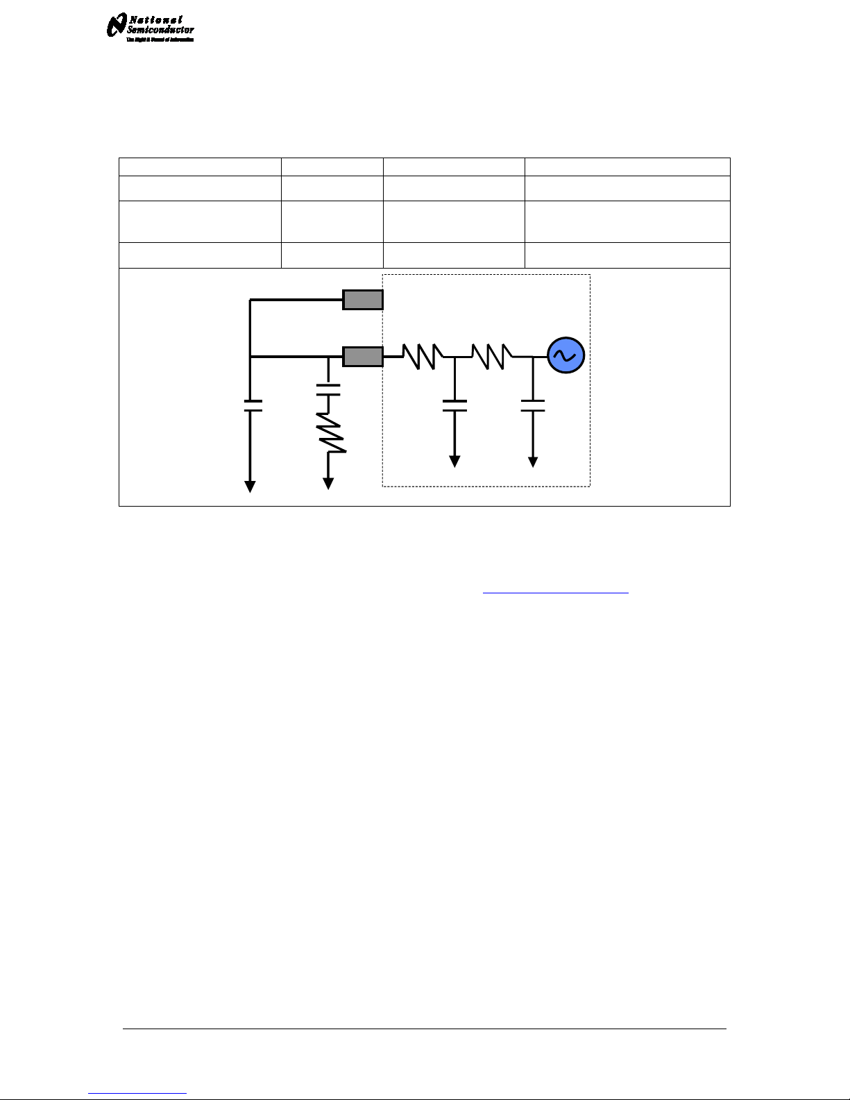
Loop Filter
Loop Bandwidth
Phase Margin
LMX2531LQ1226E EVALUATION BOARD OPERATING INSTRUCTIONS
8.0 kHz
61.3 deg
Kφ
Fcomp
1440 uA (16X)
10 MHz
Crystal Frequency
Supply Voltage
open
10 MHz
3.0 Volts
CPout
Vtune
Output Frequency
VCO Gain
20 KΩ 20 KΩ
100 nF
1KΩ
100 pF 100 pF
1184 – 1268 MHz (DIV2=0)
592 - 634 MHz (DIV2=1)
3 - 6 MHz/Volt
VCO
Quick Setup
• Install the CodeLoader software which is available at www.national.com/timing.
• Attach the parallel , or USB to parallel, port cable to the computer and the evaluation board.
• Connect 3.0 volts to the Vcc connector
• Connect the Fout connector to a spectrum analyzer or phase noise analyzer
• Connect a clean 10 MHz source to the OS Cin pin. Typically, the 10 MHz output from the back
of the RF test equipment is a good source. Signal generators tend to be very noisy and should
be used with caution. If a signal generator is used, the signal generator phase noise
contribution can be reduced by setting the signal to 80 MHz and dividing this down to a phase
detector frequency of 10 MHz.
• Set up the CodeLoader software
o Select the proper part from the menu as Select Part->PLL+VCO->LMX2531LQ1226E
o Select the proper mode from the Mode menu
o Load the part by pressing Ctrl+L or selecting Keyboard Controls->Load Device from
the menu
• It is recommended to ensure proper communication with the device
o Click the REG_RST bit on the bits/pins page and observe the current go to 0 mA
o Unclick the REG_RST bit AND press Ctrl+L. The current should be approximately
35 mA
o If device does not respond to this, consult the troubleshooting section
• When using the lower frequency band with divide by 2 enabled (DIV2=1), be aware that the
frequency programmed to the VCO is actually twice the output frequency of the device
because the VCO frequency is being divided by 2.
3

LMX2531LQ1226E EVALUATION BOARD OPERATING INSTRUCTIONS
Troubleshooting
Problem Corrective Actions
All Modes
• Ensure a valid signal is presented to the OSCin connector. If a signal
generator is used, ensure the RF is ON.
• Consult the CodeLoader instructions for more detailed information on
communication issues
Part responds to
programming, but
ise is worse
ose-in phase
Cl
no
Far-out Phase
noise is worse
Software does not communicate with the evaluation boards
does not lock to the
than evaluation
than evaluation
LPT Mode (Uses Parallel Port Cable)
• Ensure that CodeLoader is selected to LPT mode on the Port Setup tab
• Ensure the proper port number is selected (LPT1, LPT2, LPT3). CodeLoader
does NOT automatically detect this.
• Ensure the LPT cable is securely connected to the computer and board.
• Exit and Restart CodeLoader
• Ensure the parallel port is in the correct mode
o Windows often requires Administrative access to write to the parallel
port
o Ensure that the parallel port is set to “Enabled” in windows device
manager
o A reboot upon installation of CodeLoader is sometimes necessary to
get the parallel port to work.
o Standard mode is the most reliable. This can be set in the BIOS mode
of the computer as “Normal”, “Output Only”, or “AT”
USB Mode (Uses USB to Parallel Port Converter)
• On the menu, select USB->Version to verify communication with the board
• Ensure the Green LEDs are lit on the USB board
• Ensure there are no conflicts with other USB devices and reinstall the board
• Ensure that there is a valid signal presented to the OSCin connector. If a signal
generator is used, ensure that the RF is set to ON.
• If using the lower frequency band (DIV2=1), understand that the VCO
frequency in CodeLoader should be twice the frequency at the Fout pin.
• Ensure that the VCO FREQUENCY CAL bits on the Bits/Pins tab are correct
• Ensure that the loop filter is optimized if the charge pump current, phase
detector frequency, or loop filter values have been changed from their original
correct frequency
settings. Ensure that the integrated loop filter components on CodeLoader are
set to their proper settings
• Ensure the signal presented to OSCin connector is clean. Try another source,
or if it is a signal generator, try using a higher frequency and dividing it down to
the phase detector frequency.
• Ensure the OSCin signal and cable provide sufficient power level.
• If the phase detector frequency or charge pump current are lowered from their
original settings, the in-band phase noise can be degraded, even if the loop
board
instructions show
filter is re-designed for the same loop bandwidth. If the loop bandwidth is
decreased, in-band phase noise can be degraded
• Ensure the measurement equipment noise floor is not limiting the
measurement. For spectrum analyzers, the noise floor at a particular setting
can be measured by removing the RF input signal
• If the settings are changed from what the board was designed for, ensure the
delta-sigma modulator is not increasing the far-out noise. To know this, tune to
an integer channel and set the ORDER bit to “Reset Modulator”. The far out
board
instructions show
phase noise should not decrease. If it does, try a loop filter with more
attenuation or select a lower order delta-sigma modulator.
4
LMX2531LQ1226E EVALUATION BOARD OPERATING INSTRUCTIONS
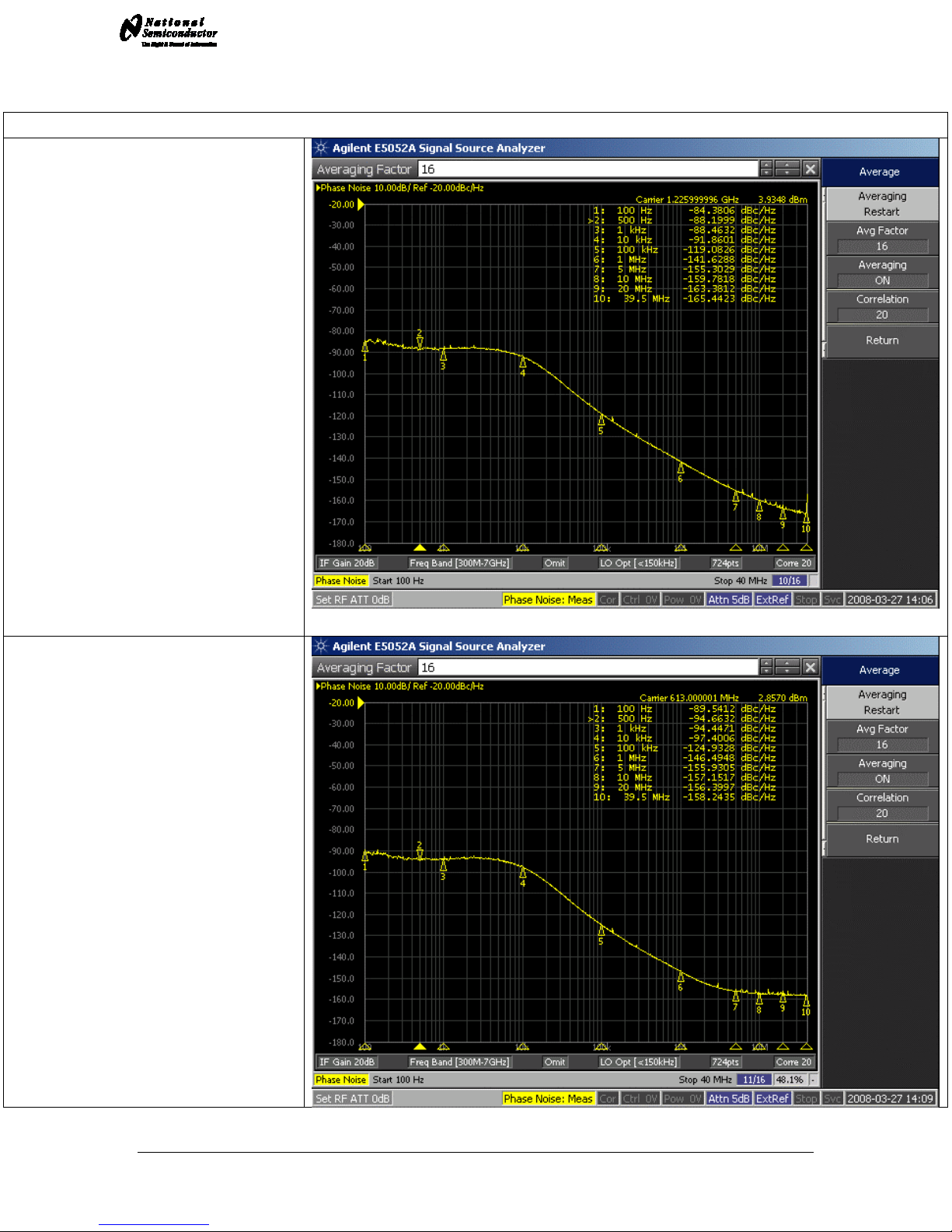
Phase Noise
Output Frequency = 1226 MHz
Internal Divide by 2 Disabled (DIV2=0)
Output Frequency = 613 MHz
Internal Divide by 2 Enabled (DIV2=1)
5

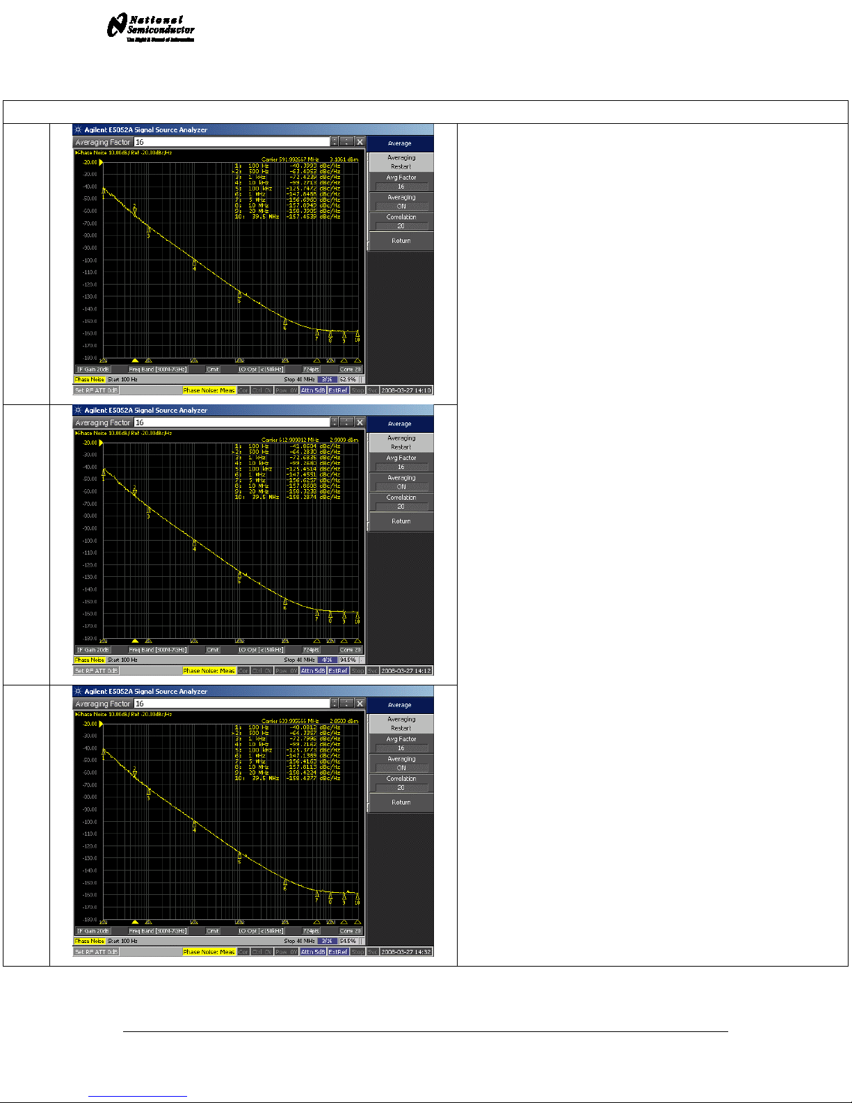
Fout = 1184 MHz
LMX2531LQ1226E EVALUATION BOARD OPERATING INSTRUCTIONS
Free-Running VCO Phase Noise (Internal Divide by 2 Disabled)
The plots to the left show the true phase noise capability of the
Fout = 1226 MHz
VCO. In order to take these plots, the E5052 phase nose
analyzer was used. The method was to lock the PLL to the
proper frequency, then disable the EN_PLL, EN_PLLLDO1, and
EN_PLLLDO2 bits. The equipment needs to be able to track
the VCO phase noise to measure in this way, and one can not
let the VCO drift too far off in frequency. If this kind of equipment
is not available, the VCO phase noise can also be measured by
making a very narrow loop bandwidth filter.
Fout = 1268 MHz
6
LMX2531LQ1226E EVALUATION BOARD OPERATING INSTRUCTIONS
Free-Running VCO Phase Noise (Internal Divide by 2 Enabled)
Fout = 592 MHz (1184 MHz/2)
The plots to the left show the true phase noise capability of the
VCO. In order to take these plots, the E5052 phase nose
analyzer was used. The method was to lock the PLL to the
proper frequency, then disable the EN_PLL, EN_PLLLDO1, and
EN_PLLLDO2 bits. The equipment needs to be able to track
the VCO phase noise to measure in this way, and one can not
let the VCO drift too far off in frequency. If this kind of equipment
is not available, the VCO phase noise can also be measured by
making a very narrow loop bandwidth filter.
When divide by 2 is enabled, the phase noise at lower offsets is
about 6 dB better; but at high offsets, the phase noise
Fout = 613 MHz (1226 MHz/2)
improvement may be less because the divider is noise floor is
adding to the phase noise.
Fout = 634 MHz (1268 MHz/2)
7
LMX2531LQ1226E EVALUATION BOARD OPERATING INSTRUCTIONS
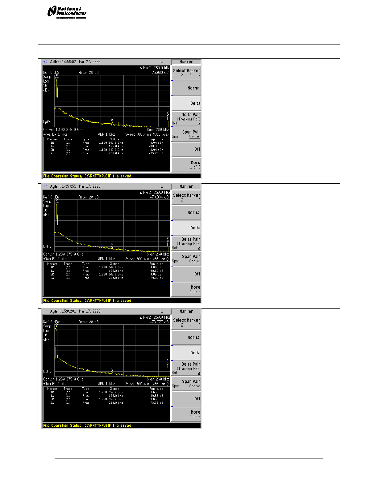
Fractional Spurs (Internal Divide by 2 Disabled)
Fractional Spur at 250 kHz offset at a
worst case frequency of 1190.25 MHz is
–75.7 dBc. Worst case channels occur
at exactly one channel spacing above or
below a multiple of the crystal frequency.
The sub-fractional spur at 125 kHz offset
of -86.4 dBc is also visible.
Fractional Spur at 250 kHz offset at a
worst case frequency of 1230.25 MHz is
–79.4 dBc.
Fractional Spur at 250 kHz offset at a
worst case frequency of 1260.25 MHz is
– 73.8 dBc.
8
 Loading...