

Page 1

查询LMX2525供应商
LMX2525
LMX2525 PLLatinum Dual Frequency Synthesizer System with Integrated VCOs
April 2004
PLLatinum
™
Dual Frequency Synthesizer System
with Integrated VCOs
General Description
LMX2525 is a highly integrated, high performance, low
power frequency synthesizer system optimized for dualband Japan PDC mobile handsets. Using a proprietary digital phase locked loop technique, LMX2525 generates very
stable, low noise local oscillator signals for up and down
conversion in wireless communications devices.
LMX2525 includes dual voltage controlled oscillators (VCOs)
for the upper and lower Japan PDC frequency bands, a loop
filter, and a fractional-N RF PLL based on a delta sigma
modulator. In concert, these blocks form a closed loop RF
synthesizer system. The RF synthesizer system supports
two frequency bands: PDC1500 and PDC800.
Serial data is transferred to the device via a three-wire
MICROWIRE interface (DATA, LE, CLK).
Operating supply voltage ranges from 2.5 V to 3.3 V.
LMX2525 features low current consumption: 10 mA at 2.8 V
when operating in the PDC800 mode.
LMX2525 is available in a 24-pin leadless leadframe package (LLP).
Features
n Small Size
5.0 mm X 4.0 mm X 0.75 mm 24-Pin LLP Package
n RF Synthesizer System
Two Integrated VCOs
Integrated Loop Filter
Low Spurious, Low Phase Noise Fractional-N RF PLL
Based on 10-Bit Delta Sigma Modulator
Frequency Resolution Down to 20 kHz
n Supports Various Reference Frequencies
12.6 MHz, 14.4 MHz, 25.2MHz, and 26.0 MHz
n Fast Lock Time: 300 µs
n Low Current Consumption
10 mA at 2.8 V in PDC800 Mode
n 2.5 V to 3.3 V Operation
n Digital Filtered Lock Detect Output
n Hardware and Software Power Down Control
Applications
n Japan PDC Systems at 800 MHz and 1500 MHz
Frequency Bands.
Functional Block Diagram
20068907
FastLock™is a trademark of National Semiconductor Corporation.
®
TRI-STATE
PLLatinum
© 2004 National Semiconductor Corporation DS200689 www.national.com
is a registered trademark of National Semiconductor Corporation.
™
is a trademark of National Semiconductor Corporation.
Page 2

Connection Diagram
LMX2525
Note: Analog ground connected through exposed die attached pad.
Pin Descriptions
Pin Number Name I/O Description
1 L1 — RF2 VCO tank pin. An external inductor is required between pins
2 L2 — RF2 VCO tank pin. An external inductor is required between pins
3 NC — Do not connect to any node on the printed circuit board.
4 NC — Do not connect to any node on the printed circuit board.
5V
6 RF1out O RF output of RF1 VCO for PDC1500
7V
8 RF2out O RF output of RF2 VCO for PDC800
9V
10 V
11 GND — Ground for digital circuitry
12 V
13 LE I MICROWIRE Latch Enable
14 DATA I MICROWIRE Data
15 CLK I MICROWIRE Clock
16 CE I Chip enable control pin
17 BS I Band select control pin
18 LD O Lock detect pin
19 V
20 OSCin I Reference frequency input
21 GND — Ground for digital circuitry
22 V
23 GND — Ground for analog circuitry
24 V
DD
DD
DD
CC
CC
CC
DD
DD
24-Pin 5x4 LLP (LQ) Package
20068902
L1 and L2 to set the resonant frequency of RF2 VCO (PDC800).
L1 and L2 to set the resonant frequency of RF2 VCO (PDC800).
— Supply voltage for RF analog circuitry
— Supply voltage for RF analog circuitry
— Supply voltage for analog circuitry
— Supply voltage for digital circuitry
— Supply voltage for digital circuitry
— Supply voltage for digital circuitry
— Supply voltage for analog circuitry
— Supply voltage for RF analog circuitry
www.national.com 2
Page 3

Ordering Information
Part Number RF1 Min.
(MHz)
LMX2525LQX1321 1270.22 1394.95~1321 633.15 768.00 25251321 4500 units on
LMX2525LQ1321 1270.22 1394.95~1321 633.15 768.00 25251321 1000 units on
RF1 Max.
(MHz)
RF1
Center
(MHz)
RF2 Min.
(MHz)
RF2 Max.
(MHz)
Package
Marking
Part Number Description
20068903
Typical Application Circuit (Note 1)
LMX2525
Supplied As
tape and reel
tape and reel
20068904
Note 1: Refer to RF2 VCO Tuning Range vs. External Inductance plot to aid in selecting the appropriate external inductance, PCB trace and L1, for the desired
frequency range.
www.national.com3
Page 4

Absolute Maximum Ratings (Notes 2, 3,
4)
LMX2525
If Military/Aerospace specified devices are required,
please contact the National Semiconductor Sales Office/
Distributors for availability and specifications.
Parameter Symbol Ratings Units
Supply Voltage V
Voltage on any pin
to GND
Storage Temperature Range T
CC,VDD
V
I
STG
-0.5 to 3.6 V
-0.3 to VCC+ 0.3 V
-0.3 to V
-65 to 150 ˚C
+ 0.3 V
DD
Recommended Operating
Conditions
Parameter Symbol Min Typ Max Unit
Ambient Temperature T
Supply Voltage (to GND) V
Note 2: Absolute Maximum Ratings indicate limits beyond which damage to
the device may occur. Recommended Operating Conditions indicate conditions for which the device is intended to be functional, but do not guarantee
specific performance limits. For guaranteed specifications and test conditions, refer to the Electrical Characteristics section. The guaranteed specifications apply only for the conditions listed.
Note 3: This device is a high performance RF integrated circuit with an ESD
<
rating
2 kV and is ESD sensitive. Handling and assembly of this device
should be done at ESD protected workstations.
Note 4: GND=0V.
A
CC,VDD
-30 25 85 ˚C
2.5 3.3 V
Electrical Characteristics (V
= 25 ˚C; Limits in boldface type apply over the operating temperature range from -20 ˚C ≤ TA≤ 75 ˚C unless other-
for T
A
= 2.8 V, refer to Typical Application Circuit; Limits in standard typeface are
IN
wise noted.)
Symbol Parameter Condition Min Typ Max Units
I
PARAMETERS
CC
I
CC+IDD
Supply Current (Note 5) OB_CRL [1:0] = 10 10.6 12.0
mA
12.3
OB_CRL [1:0] = 00 10.0 11.5
mA
11.8
I
CC+IDD
Supply Current (Note 6) OB_CRL [1:0] = 10 15.0 16.5
mA
16.8
OB_CRL [1:0] = 00 14.2 15.6
mA
15.9
I
PD
Power Down Current CE = LOW or
20 µA
RF_PD = 1
REFERENCE OSCILLATOR PARAMETERS
f
OSCin
V
OSCin
Reference Oscillator Input Frequency
(Note 7)
Supports 12.6, 14.4, 25.2
and 26.0 MHz.
12.6 14.4 26.0 MHz
Reference Oscillator Input Sensitivity 0.5 V
CC
Vp-p
RF1 VCO FOR PDC1500
f
RF1out
P
RF1out
Frequency Range (Note 8) RF1 VCO for PDC1500 1270.22 1394.95 MHz
Output Power OB_CRL [1:0] = 11 -5 -2 1 dBm
OB_CRL [1:0] = 10 -7 -4 -1 dBm
OB_CRL [1:0] = 01 -10 -7 -4 dBm
OB_CRL [1:0] = 00 -13 -10 -7 dBm
Lock Time Full frequency span within
each band in High Speed
300
(Note 9)
µs
Mode (HS = 1).
Between bands High Speed
Mode (HS = 1).
Full frequency span within
each band in Normal Mode
(HS = 0).
(Note 11)
Between bands in Normal
Mode (HS = 0).
300
(Note 9)
500
(Note 9)
375
(Note 10)
500
(Note 9)
400
µs
µs
µs
µs
µs
(Note 10)
RMS Phase Error 1.3 degrees
www.national.com 4
Page 5

LMX2525
Electrical Characteristics (V
= 25 ˚C; Limits in boldface type apply over the operating temperature range from -20 ˚C ≤ TA≤ 75 ˚C unless otherwise
T
A
= 2.8 V, refer to Typical Application Circuit; Limits in standard typeface are for
IN
noted.) (Continued)
Symbol Parameter Condition Min Typ Max Units
RF1 VCO FOR PDC1500
L(f)
RF1out
Phase Noise when RF1 VCO for
PDC1500 is activated in Normal
Mode (HS = 0).
@
25 kHz offset -95 -93
@
50 kHz offset -106 -103
dBc/Hz
-91
dBc/Hz
-101
@
100 kHz offset -115 -113
dBc/Hz
-111
@
1 MHz offset -135
dBc/Hz
-133
2ndHarmonic Suppression -25 dBc
rd
3
Harmonic Suppression OB_CRL [1:0] = 11, 10, 01 -20 dBc
OB_CRL [1:0] = 00 -14
dBc
-11
Spurious Tones
@
≤ 25 kHz offset -45 dBc
@
25 kHz<offset ≤ 50 kHz -60 dBc
@
50 kHz<offset ≤ 100 kHz -69 dBc
@
offset>100 kHz -75 dBc
RF2 VCO FOR PDC800
f
RF2out
P
RF2out
Frequency Range (Note 8) RF2 VCO for PDC800 633.15 768.00 MHz
Output Power OB_CRL [1:0] = 11 -6 -3 0 dBm
OB_CRL [1:0] = 10 -9 -6 -3 dBm
OB_CRL [1:0] = 01 -11 -8 -5 dBm
OB_CRL [1:0] = 00 -15 -12 -9 dBm
Lock Time Full frequency span within
each band in High Speed
300
(Note 9)
µs
Mode (HS = 1).
Between bands High Speed
Mode (HS = 1).
Full frequency span within
each band in Normal Mode
(HS = 0).
(Note 11)
Between bands in Normal
Mode (HS = 0).
300
(Note 9)
500
(Note 9)
375
(Note 10)
500
(Note 9)
400
µs
µs
µs
µs
µs
(Note 10)
RMS Phase Error 1.3 degrees
L(f)
RF2out
Phase Noise when RF2 VCO for
PDC800 is activated in Normal Mode
(HS = 0).
@
25 kHz offset -95 -93
@
50 kHz offset -106 -103
dBc/Hz
-91
dBc/Hz
-101
@
100 kHz offset -115 -113
dBc/Hz
-111
@
1 MHz offset -135
dBc/Hz
-133
nd
Harmonic Suppression -25 dBc
2
rd
3
Harmonic Suppression OB_CRL[1:0] = 11, 10, 01 -20 dBc
OB_CRL[1:0] = 00 -14
dBc
-11
www.national.com5
Page 6

Electrical Characteristics (V
= 25 ˚C; Limits in boldface type apply over the operating temperature range from -20 ˚C ≤ TA≤ 75 ˚C unless otherwise
T
A
noted.) (Continued)
LMX2525
= 2.8 V, refer to Typical Application Circuit; Limits in standard typeface are for
IN
Symbol Parameter Condition Min Typ Max Units
RF2 VCO FOR PDC800
Spurious Tones
@
≤ 25 kHz offset -45 dBc
@
25 kHz<offset ≤ 50 kHz -60 dBc
@
50 kHz<offset ≤ 100 kHz -69 dBc
@
offset>100 kHz -75 dBc
DIGITAL INTERFACE (DATA, CLK, LE, LD, CE, BS)
V
IH
V
IL
I
IH
I
IL
High-Level Input Voltage 0.8 V
0.8 V
CC
DD
Low-Level Input Voltage -0.3 0.2 V
-0.3 0.2 V
V
CC
V
DD
CC
DD
High-Level Input Current -10 10 µA
Low-Level Input Current -10 10 µA
Input Capacitance 3 pF
Rise/Fall Time 30 ns
V
OH
V
OL
High-Level Output Voltage VCC- 0.4 V
V
- 0.4 V
DD
Low-Level Output Voltage 0.4 V
Output Capacitance 5pF
MICROWIRE INTERFACE TIMING
t
CS
t
CH
t
CWH
t
CWL
t
DS
Data to Clock Set Up Time 50 ns
Data to Clock Hold Time 10 ns
Clock Pulse Width HIGH 50 ns
Clock Pulse Width LOW 50 ns
Latch Enable LOW to Data Set Up
50 ns
Time
t
ES
t
EW
Note 5: RF PLL and VCO in PDC800 mode.
Note 6: RF PLL and VCO in PDC1500 mode.
Note 7: The reference frequency must be programmed using the OSC_FREQ control bit. For other reference frequencies, please contact National Semiconductor.
Note 8: For other frequency ranges, please contact National Semiconductor.
Note 9: Lock time is defined as the time difference between the beginning of the frequency transition and the point at which the frequency remains within +/-1 kHz
of the final frequency.
Note 10: Lock time is defined as the time difference between the beginning of the frequency transition and the point at which the frequency remains within +/-3 kHz
of the final frequency.
Note 11: Lock time specification also applies to power up with MICROWIRE serial interface.
Note 12: All limits are guaranteed. All electrical characteristics having room temperature limits are tested during production with T
Statistical Quality Control (SQC) methods. All hot and cold limits are guaranteed by correlating the electrical characteristics to process and temperature variations
and applying statistical process control.
Clock to Latch Enable Set Up Time 50 ns
Latch Enable Pulse Width 50 ns
= 25 ˚C or correlated using
A
V
V
V
V
www.national.com 6
Page 7
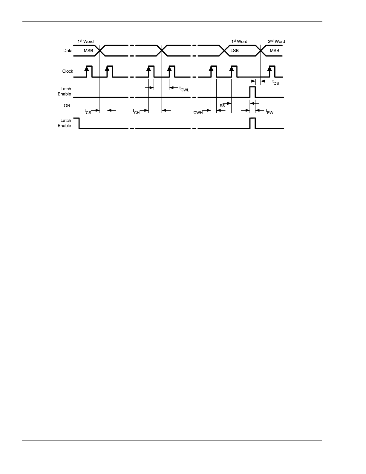
MICROWIRE Interface Timing Diagram
LMX2525
20068901
www.national.com7
Page 8

Typical Performance Characteristics (Note 13)
LMX2525
Note 13: Typical performance characteristics do not guarantee specific performance limits. For guaranteed specifications, refer to the Electrical Characteristics
section.
Note 14: The frequency range is defined as the difference between the highest frequency and the lowest frequency of a given unit. For a chosen external
inductance, the typical frequency range equals the difference between the Typical Maximum Frequency and the Typical Minimum Frequency. Typical frequency
range may be assumed on any unit with that chosen external inductance, even if the unit has worst case Maximum Frequency or worst case Minimum Frequency.
RF2 VCO Tuning Range vs. External Inductance (Note 14)
= 2.8 V
V
IN
20068911
www.national.com 8
Page 9

Functional Description
GENERAL
The LMX2525 is a highly integrated frequency synthesizer
system for Japan PDC wireless communication systems.
The LMX2525 supports dual band operation for 800 MHz
and 1500 MHz.
The LMX2525 includes all functional blocks for the RF PLL
including RF VCOs, frequency dividers, PFDs, and loop
filters. Only external passive elements for the RF2 VCO tank
and supply bypassing are required to complete the RF synthesizer.
The LMX2525 uses a patent pending Fractional-N synthesizer architecture based on a delta sigma modulator to support fine frequency resolution. Four of the most common
reference frequencies for PDC applications, 12.6 MHz, 14.4
MHz, 25.2 MHz and 26.0 MHz, are supported. The unique
feature of this architecture is its low spurious modulation
effect.
The use of a fractional synthesizer based on a delta sigma
modulator allows for faster lock and system set-up times,
which reduces system power consumption. The loop filter is
included on chip to minimize the external noise coupling and
to reduce the form factor applicable to the board level application. Only one of the two RF VCOs is activated at a given
time, and each output is provided through its own output pin.
20068910
where C
is the total capacitance of the VCO, including
total
the parasitic capacitance and the nominal self-tuning capacitance. Note, the external inductance consists of the PCB
traces and lumped element inductor. The output frequency
tuning range can be optimized for the specific application by
selecting the appropriate external inductance. Refer to RF2
VCO Tuning Range vs. External Inductance plot to aid in
selecting the appropriate external inductance. Care should
be taken to ensure proper frequency coverage when choosing the tolerance of the lumped element inductor. For the
1500 MHz band, the internal bonding-wires provide the necessary inductance to set the VCO center frequency.
LMX2525
RF PLL SECTION
Frequency Selection
The divide ratio can be calculated using the following equations:
= {8 x RF_B + RF_A+ (RF_FN / FD)} x (f
f
VCO
<
(RF_A
f
VCO
(RF_A
f
VCO
RF_B) for PDC1500
= {4 x RF_B + RF_A+ (RF_FN / FD)} x (f
<
RF_B) for PDC800
: Output frequency of voltage controlled oscillator (VCO)
OSC
OSC
/ R) where
/ R) where
RF_B: Preset divide ratio of binary 4-bit programmable
counter (2 ≤ RF_B ≤ 15)
RF_A: Preset divide ratio of binary 3-bit swallow counter (0 ≤
RF_A ≤ 7 for PDC1500 and 0 ≤ RF_A ≤ 3 for PDC800)
RF_FN: Preset numerator of binary 10-bit modulus counter
<
(0 ≤ RF_FN
FD: Preset denominator for modulus counter (FD = f
) where fCHis the channel spacing)
Xf
CH
: Reference oscillator frequency
f
OSC
FD)
OSC
/(R
R: Internal reference oscillator frequency divider (1 for 12.6
MHz and 14.4 MHz, 2 for 25.2 MHz and 26.0 MHz)
The denominator, FD, in the above equation is dependent on
the channel spacing and reference oscillator frequency. The
channel spacing will change based on the Rx/Tx and BS
bits. Table 6 in the R0 Register section summarizes the
values of FD.
VCO Frequency Tuning
The center frequency of the RF VCOs are determined by the
resonant frequency of the tank circuit, illustrated in Figure 1.
With an internal fixed bonding-wire inductor and an external
inductance, the center frequency of the VCO is given as
follows:
20068905
FIGURE 1. External Inductor Connection
In real implementation, the inductance of L
fixed
and L
external
can vary from its nominal value. The LMX2525 utilizes a
built-in tracking algorithm to compensate for variations up to
±
15% and tunes the VCO to the required frequency. During
the frequency acquisition period, the loop bandwidth is extended to achieve the frequency lock. After the frequency
lock, the loop bandwidth of the PLL is set to the nominal
value and the phase lock is achieved. The transition between the two operating modes is very smooth and extremely fast to meet the stringent PDC requirements for lock
time and phase noise.
POWER DOWN MODE
The LMX2525 includes the power down mode to reduce the
power consumption. The LMX2525 enters the power down
mode either by taking the CE pin LOW or by setting the
RF_PD bit in the R0 register. If the CE pin is set LOW, the
circuit is powered down regardless of the register values.
When the CE pin is HIGH, the RF_PD bit controls power to
the RF circuitry. Data can be written to the registers even
when the CE pin is set LOW. The following truth table
summarizes the power down logic.
TABLE 1. Power Down Modes
CE Pin RF_PD Bit Mode
HIGH 0 Active
HIGH 1 Not Active
LOW 0 Not Active
LOW 1 Not Active
www.national.com9
Page 10

Functional Description (Continued)
BAND SELECT MODE
LMX2525
The BS pin and BS bit can be used to select one of the two
RF VCO outputs. When using the BS pin, the BS bit must be
set to 0, and when using the BS bit, the BS pin must be tied
to ground. When using the BS pin, the state of the input must
exceed the minimum band select set up time prior to the LE
signal transition. The truth table summarizing the band select
logic is as follows:
on the LD pin. When the PLL is not locked, the LD pin
remains LOW. After obtaining phase lock, the LD pin will
have a logical HIGH level. The LD output is always LOW
when the LD register bit is 0 and in power down mode.
TABLE 3. Lock Detect Modes
LD Bit Mode
0 Disable (GND)
1 Enable
TABLE 2. Band Select Modes
BS Pin BS Bit Mode
HIGH 0 PDC1500
LOW 0 PDC800
LOW 1 PDC1500
LOCK DETECT MODE
The LD output can be used to indicate the lock status of the
PLL. Bit 6 in Register R1 determines the signal that appears
FIGURE 2. Lock Detect Timing Diagram Waveform (Notes 15, 16, 17, 18, 19)
TABLE 4. Lock Detect Logic
RF PLL Section LD Output
Locked HIGH
Not Locked LOW
20068908
Note 15: LD output becomes LOW when the phase error is larger than tW2.
Note 16: LD output becomes HIGH when the phase error is less than t
four or more consecutive cycles.
Note 17: Phase Error is determined on the leading edge. Only errors greater
than t
and tW2are labeled.
W1
www.national.com 10
W1
for
Note 18: t
both bands.
Note 19: The lock detect comparison occurs with every 64
f
.
N
is 5 ns for PDC1500 and 10 ns for PDC800. tW2is 10 ns for
W1
th
cycle of fRand
Page 11

Functional Description (Continued)
LMX2525
FIGURE 3. Lock Detect Flow Diagram
LOCKING MODES
Two frequency-locking modes are provided: a Normal mode
and a High Speed mode for faster lock times. The HS bit in
register R0 controls the locking mode.
TABLE 5. Locking Modes
HS Bit Mode
0 Normal mode
1 High Speed mode
20068909
MICROWIRE INTERFACE
The programmable register set is accessed via the
MICROWIRE serial interface. The interface is comprised of
three signal pins: CLK, DATA, and LE (Latch Enable). Serial
data is clocked into the 24-bit shift register on the rising edge
of the clock. The last bits decode the internal control register
address. When the latch enable (LE) transitions from LOW
to HIGH, data stored in the shift registers is loaded into the
corresponding control register. The data is loaded MSB first.
www.national.com11
Page 12

Programming Description
GENERAL PROGRAMMING INFORMATION
LMX2525
The serial interface has a 24-bit shift register to store the incoming data bits temporarily. The incoming data is first loaded into the
shift register from MSB to LSB. The data is shifted at the rising edge of the clock signal. When the latch enable signal transitions
from LOW to HIGH, the data stored in shift register is transferred to the proper register depending on the address bit setting. The
selection of the particular register is determined by the control bits indicated in boldface text.
At initial start-up, the MICROWIRE loading requires three default words (registers R2, loaded first, to R0, loaded last). After the
device has been initially programmed, the RF VCO frequency can be changed using a single register (R0).
The control register content map describes how the bits within each control register are allocated to the specific control functions.
COMPLETE REGISTER MAP
MSB SHIFT REGISTER BIT LOCATION LSB
Register
R0
(Default)
R1
(Default)
R2
(Default)
R3 1 0 0 00 1101000000000 0 1 1 01 1
R4 0 0 0 00 0111010001100 1 0 011 1
R5 0 0 0 00 0000000000000 0 0111 1
Note: R0 control register will be used when hot start frequency change.
Note: Boldface text represent address bits.
23 22 21 2019 1817161514131211109876 5 4 3 2 1 0
RX/TXRF_PDHS 0 BS RF_B
[3:0]
SPI_
0 0 10 010100000010LDOB_
DEF
1 1 0 01 0000111100000 0 0 0 1 10
RF_A
[2:0]
RF_FN
[9:0]
CRL
[1:0]
OSC_
FREQ
[1:0]
00
01
www.national.com 12
Page 13
Programming Description (Continued)
R0 REGISTER
The R0 register address bits (R0 [1:0]) are “00”.
The Rx/Tx bit selects between receive and transmit modes and, in conjunction with the band select bit (BS), the channel spacing
to be synthesized.
The RF_PD bit selects the power down mode of the RF PLL and selected VCO.
The HS bit selects between normal and high speed locking mode.
The BS bit determines which of the two internal VCOs (PDC800 or PDC1500) is active.
The RF N counter consists of the 4-bit programmable counter (RF_B counter), the 3-bit swallow counter (RF_A counter) and the
10-bit delta sigma modulator (RF_FN counter). The equations for calculating the counter values are presented below.
R0 REGISTER
MSB SHIFT REGISTER BIT LOCATION LSB
23 22 21 2019 181716151413121110987654321 0
Data Field Address
Register
R0
(Default)
RX/TXRF_PDHS 0 BS RF_B
[3:0]
Name Functions
RX/TX RX/TX Mode
RF_PD Power Down of RF Synthesizer
HS Locking Mode
BS Band Select
RF_B [3:0] RF_B Counter
RF_A [2:0] RF_A Counter
RF_FN [9:0] RF_FN Counter
RF_A
[2:0]
0=Rx
1=Tx
0 = RF synthesizer on (Active mode)
1 = RF synthesizer powered down
0 = Normal Mode
1 = High Speed Mode
1 = RF1 VCO (PDC1500)
0 = RF2 VCO (PDC800)
4-bit programmable counter
0 ≤ RF_B ≤ 15 for both bands
3-bit swallow counter
0 ≤ RF_A ≤ 7 for PDC1500
0 ≤ RF_A ≤ 3 for PDC800
10-bit modulus counter
<
0 ≤ RF_FN
FD See Table 6 for FD values.
RF_FN
[9:0]
Field
00
LMX2525
Counter Name Symbol Functions
Modulus Counter RF_FN RF N Divider
Programmable Counter RF_B
Swallow Counter RF_A
N=8xRF_B + RF_A + RF_FN/FD (PDC1500)
N=4xRF_B + RF_A + RF_FN/FD (PDC800)
www.national.com13
Page 14

Programming Description (Continued)
PULSE SWALLOW FUNCTION
LMX2525
f
= {8 x RF_B + RF_A + (RF_FN / FD)} x f
VCO
= {4 x RF_B + RF_A + (RF_FN / FD)} x f
f
VCO
: Output frequency of voltage controlled oscillator (VCO)
f
VCO
RF_B: Preset divide ratio of binary 4-bit programmable counter (2 ≤ RF_B≤ 15)
RF_A: Preset divide ratio of binary 3-bit swallow counter (0 ≤ RF_A ≤ 7 for PDC1500 and 0 ≤ RF_A ≤ 3 for PDC800)
RF_FN: Preset numerator of binary 10-bit modulus counter (0 ≤ RF_FN
FD: Preset denominator for modulus counter (FD = f
f
: Reference oscillator frequency
OSC
R: Internal reference oscillator frequency divider
OSC_FREQ [1:0] Reference Oscillator Frequency (MHz) R Divider
00 12.6 1
01 14.4 1
10 25.2 2
11 26.0 2
The value of the denominator (FD) is depended on the channel spacing and reference oscillator frequency. Table 6 summarizes
the denominator values based on the settings of the Rx/Tx, BS, and OSC_FREQ [1:0] bits.
Rx/Tx BS OSC_FREQ [1:0] Reference Oscillator Frequency (MHz) R fCH(kHz) Denominator(FD)
0 0 00 12.6 1 25.0 504
0 0 01 14.4 1 25.0 576
0 0 10 25.2 2 25.0 504
0 0 11 26.0 2 25.0 520
0 1 00 12.6 1 25.0 504
0 1 01 14.4 1 25.0 576
0 1 10 25.2 2 25.0 504
0 1 11 26.0 2 25.0 520
1 0 00 12.6 1 20.0 630
1 0 01 14.4 1 20.0 720
1 0 10 25.2 2 20.0 630
1 0 11 26.0 2 20.0 650
1 1 00 12.6 1 22.22 567
1 1 01 14.4 1 22.22 648
1 1 10 25.2 2 22.22 567
1 1 11 26.0 2 22.22 585
/ R where (RF_A<RF_B) for PDC1500
OSC
/ R where (RF_A<RF_B) for PDC800
OSC
<
FD)
/(RxfCH) where fCHis the channel spacing)
OSC
TABLE 6. Demonimator Values
www.national.com 14
Page 15

Programming Description (Continued)
R1 REGISTER
The R1 register address bits (R1 [1:0]) are “01”.
The SPI_DEF bit allows for the programming of words R3 to R5. Under most circumstances, the SPI_DEF bit should be set to
1.
The LD bit sets the function of the lock detect pin. Enabling the lock detect function provides a digital lock detect output of the
active RF synthesizer at the LD pin.
The OB_CRL [1:0] bits determine the power level of the RF output buffer. The power level can be adjusted to best meet the
system requirement. Refer to the Electrical Characteristics section for power output specifications.
The reference frequency selection bits, OSC_FREQ [1:0], are used to set the reference clock and R divider for use with one of
the following reference frequencies: 12.6 MHz, 14.4 MHz, 25.2 MHz or 26.0 MHz. The LMX2525 uses the OSC_FREQ bits along
with the BS and RX/TX bits to determine the correct divide ratios needed to meet the required channel spacing for the mode of
operation selected. Refer to Table 6 for a summary of denominator values.
R1 REGISTER
MSB SHIFT REGISTER BIT LOCATION LSB
23 222120191817161514131211109876 5 4 3 2 1 0
Data Field Address
Register
R1
(Default)
SPI_
0010010100000010LDOB_
DEF
CRL
[1:0]
OSC_
FREQ
[1:0]
Field
01
LMX2525
Name Functions
SPI_DEF Default Register Selection
0 = OFF (Use values set in R0 to R5)
1 = ON (Use default values set in R0 to R2)
LD Lock Detect
0 = Disable (GND)
1 = Enable
OB_CRL [1:0] Output Buffer Control
00 = Minimum Output Power
01 =
10 =
11 = Maximum Output Power
OSC_FREQ [1:0] Reference Frequency Selection
00 = 12.6 MHz
01 = 14.4 MHz
10 = 25.2 MHz
11 = 26.0 MHz
www.national.com15
Page 16

Programming Description (Continued)
R2 REGISTER
LMX2525
The R2 register address bits (R2 [1:0]) are “10”.
R2 REGISTER
MSB SHIFT REGISTER BIT LOCATION LSB
23 22212019181716151413121110987654321 0
Data Field Address
Register
R2
(Default)
R3 REGISTER
The R3 register address bits (R3 [2:0]) are “011”. This register is only written to if the SPI_DEF bit is set to 0.
Register
R3 1 0000110100000000001101 1
1 10010000111100000000110
R3 REGISTER
MSB SHIFT REGISTER BIT LOCATION LSB
23 22212019181716151413121110987654321 0
Data Field Address
Field
Field
R4 REGISTER
The R4 register address bits (R4 [3:0]) are “0111”. This register is only written to if the SPI_DEF bit is set to 0.
R4 REGISTER
MSB SHIFT REGISTER BIT LOCATION LSB
23 22212019181716151413121110987654321 0
Data Field Address
Register
R4 0 0000011101000110010011 1
R5 REGISTER
The R5 register address bits (R5 [4:0]) are “01111”. This register is only written to if the SPI_DEF bit is set to 0.
R5 REGISTER
MSB SHIFT REGISTER BIT LOCATION LSB
23 22212019181716151413121110987654321 0
Register
R5 0 0000000000000000000111 1
Data Field Address Field
Field
www.national.com 16
Page 17

Physical Dimensions inches (millimeters) unless otherwise noted
LMX2525 PLLatinum Dual Frequency Synthesizer System with Integrated VCOs
24-Pin Leadless Leadframe Package (LLP)
Order Number LMX2525
NSC Package Number LQA24A
LIFE SUPPORT POLICY
NATIONAL’S PRODUCTS ARE NOT AUTHORIZED FOR USE AS CRITICAL COMPONENTS IN LIFE SUPPORT
DEVICES OR SYSTEMS WITHOUT THE EXPRESS WRITTEN APPROVAL OF THE PRESIDENT AND GENERAL
COUNSEL OF NATIONAL SEMICONDUCTOR CORPORATION. As used herein:
1. Life support devices or systems are devices or
systems which, (a) are intended for surgical implant
into the body, or (b) support or sustain life, and
whose failure to perform when properly used in
accordance with instructions for use provided in the
2. A critical component is any component of a life
support device or system whose failure to perform
can be reasonably expected to cause the failure of
the life support device or system, or to affect its
safety or effectiveness.
labeling, can be reasonably expected to result in a
significant injury to the user.
BANNED SUBSTANCE COMPLIANCE
National Semiconductor certifies that the products and packing materials meet the provisions of the Customer Products
Stewardship Specification (CSP-9-111C2) and the Banned Substances and Materials of Interest Specification
(CSP-9-111S2) and contain no ‘‘Banned Substances’’ as defined in CSP-9-111S2.
National Semiconductor
Americas Customer
Support Center
Email: new.feedback@nsc.com
Tel: 1-800-272-9959
www.national.com
National does not assume any responsibility for use of any circuitry described, no circuit patent licenses are implied and National reserves the right at any time without notice to change said circuitry and specifications.
National Semiconductor
Europe Customer Support Center
Fax: +49 (0) 180-530 85 86
Email: europe.support@nsc.com
Deutsch Tel: +49 (0) 69 9508 6208
English Tel: +44 (0) 870 24 0 2171
Français Tel: +33 (0) 1 41 91 8790
National Semiconductor
Asia Pacific Customer
Support Center
Email: ap.support@nsc.com
National Semiconductor
Japan Customer Support Center
Fax: 81-3-5639-7507
Email: jpn.feedback@nsc.com
Tel: 81-3-5639-7560
 Loading...