

National Semiconductor LMX2505 Technical data
查询LMX2505供应商
LMX2505
LMX2505 PLLatinum Dual Frequency Synthesizer System with Integrated VCOs
April 2004
PLLatinum
™
Dual Frequency Synthesizer System
with Integrated VCOs
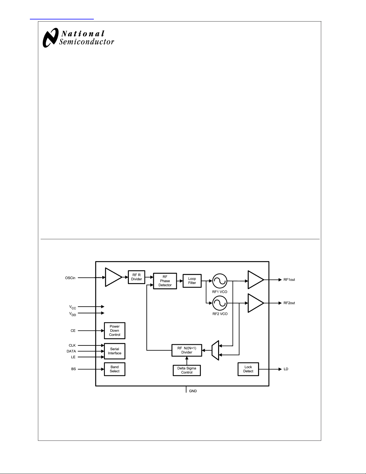
General Description
LMX2505 is a highly integrated, high performance, low
power frequency synthesizer system optimized for dualband Japan PDC mobile handsets. Using a proprietary digital phase locked loop technique, LMX2505 generates very
stable, low noise local oscillator signals for up and down
conversion in wireless communications devices.
LMX2505 includes dual voltage controlled oscillators (VCOs)
for the upper and lower Japan PDC frequency bands, a loop
filter, and a fractional-N RF PLL based on a delta sigma
modulator. In concert these blocks form a closed loop RF
synthesizer system. The RF synthesizer system supports
two frequency bands: PDC1500 and PDC800.
Serial data is transferred to the device via a three-wire
MICROWIRE interface (DATA, LE, CLK).
Operating supply voltage ranges from 2.5 V to 3.3 V.
LMX2505 features low current consumption: 10 mA at 2.8 V
when operating in the PDC800 mode.
LMX2505 is available in a 28-pin leadless leadframe package (LLP).
Features
n Small Size
5.0 mm X 5.0 mm X 0.75 mm 28-Pin LLP Package
n RF Synthesizer System
Two Integrated VCOs
Integrated Loop Filter
Low Spurious, Low Phase Noise Fractional-N RF PLL
Based on 10-Bit Delta Sigma Modulator
Frequency Resolution Down to 20 kHz
n Supports Various Reference Frequencies
12.6/14.4/25.2/26.0 MHz
n Fast Lock Time: 300 µs
n Low Current Consumption
10 mA at 2.8 V in PDC800 Mode
n 2.5 V to 3.3 V Operation
n Digital Filtered Lock Detect Output
n Hardware and Software Power Down Control
Applications
n Japan PDC Systems at 800 MHz and 1500 MHz
Frequency Bands.
Functional Block Diagram
20067107
FastLock™is a trademark of National Semiconductor Corporation.
®
TRI-STATE
PLLatinum
© 2004 National Semiconductor Corporation DS200671 www.national.com
is a registered trademark of National Semiconductor Corporation.
™
is a trademark of National Semiconductor Corporation.

Connection Diagram
LMX2505
NOTE: Analog ground connected through exposed die attached pad.
Pin Descriptions
Pin Number Name I/O Description
1 OSCin I Reference frequency input
2 GND — Ground for digital circuitry
3V
4 GND — Ground for analog circuitry
5 NC — Do not connect to any node on the printed circuit board.
6 NC — Do not connect to any node on the printed circuit board.
7V
8 NC — Do not connect to any node on the printed circuit board.
9 L1 — RF2 VCO tank pin. An external inductor is required between pins
10 L2 — RF2 VCO tank pin. An external inductor is required between pins
11 NC — Do not connect to any node on the printed circuit board.
12 NC — Do not connect to any node on the printed circuit board.
13 V
14 RF1out O RF output of RF1 VCO for PDC1500
15 V
16 RF2out O RF output of RF2 VCO for PDC800
17 V
18 GND — Ground for digital circuitry
19 V
20 GND — Ground for digital circuitry
21 V
22 LE I MICROWIRE Latch Enable
23 DATA I MICROWIRE Data
24 CLK I MICROWIRE Clock
25 CE I Chip enable control pin
26 BS I Band select control pin
27 LD O Lock detect pin
28 V
DD
DD
DD
DD
DD
CC
CC
CC
28-Pin 5x5 LLP (LQ) Package
20067102
— Supply voltage for analog circuitry
— Supply voltage for RF analog circuitry
L1 and L2 to set the resonant frequency of RF2 VCO (PDC800).
L1 and L2 to set the resonant frequency of RF2 VCO (PDC800).
— Supply voltage for RF analog circuitry
— Supply voltage for RF analog circuitry
— Supply voltage for analog circuitry
— Supply voltage for digital circuitry
— Supply voltage for digital circuitry
— Supply voltage for digital circuitry
www.national.com 2
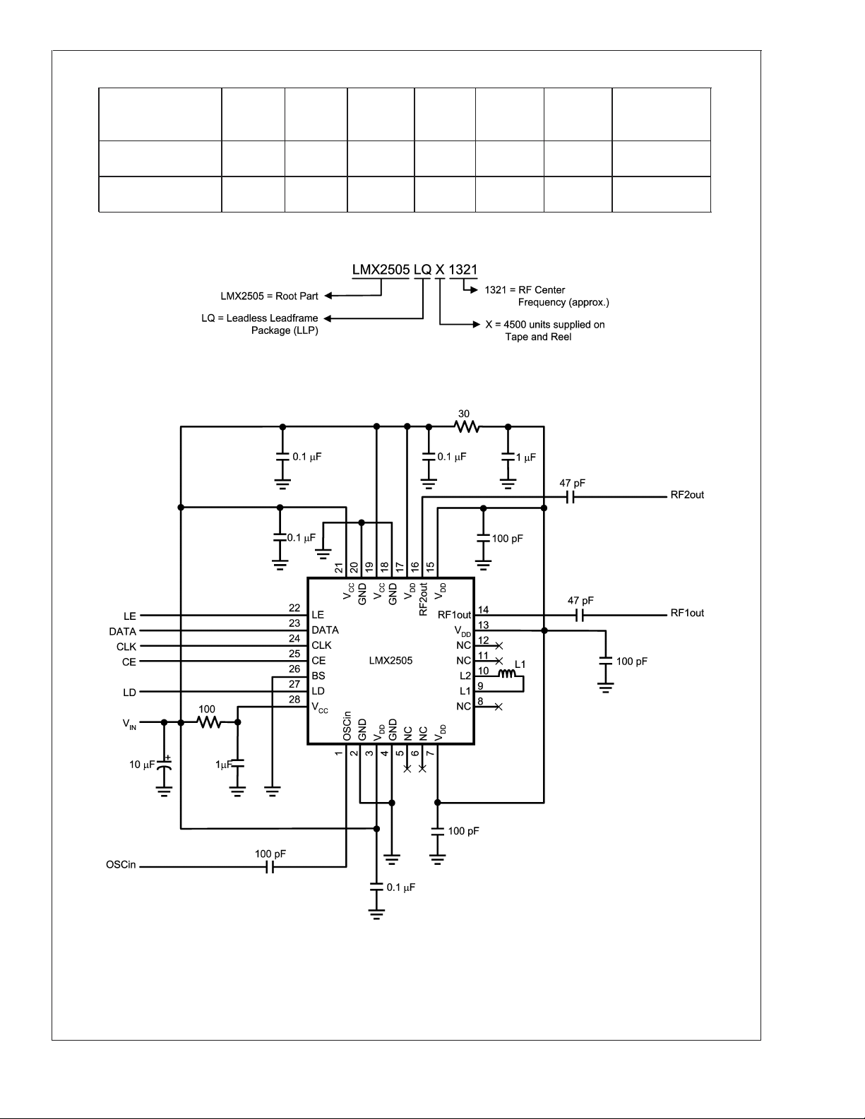
Ordering Information
Part Number RF1 Min.
(MHz)
LMX2505LQX1321 1270.22 1394.95~1321 633.15 768.0 25051321 4500 units on
LMX2505LQ1321 1270.22 1394.95~1321 633.15 768.0 25051321 1000 units on
RF1 Max.
(MHz)
RF1
Center
(MHz)
RF2 Min.
(MHz)
RF2 Max.
(MHz)
Package
Marking
Part Number Description
20067103
Typical Application Circuit (Note 1)
LMX2505
Supplied As
tape and reel
tape and reel
20067104
Note 1: Refer to RF2 VCO Tuning Range vs. External Inductance plot to aid in selecting the appropriate external inductance, PCB trace and L1, for the desired
frequency range.
www.national.com3
Absolute Maximum Ratings (Notes 2, 3,
4)
LMX2505
If Military/Aerospace specified devices are required,
please contact the National Semiconductor Sales Office/
Distributors for availability and specifications.
Parameter Symbol Ratings Units
Supply Voltage V
Voltage on any pin
to GND
Storage Temperature
Range
CC,VDD
V
I
T
STG
-0.5 to 3.6 V
-0.3 to VCC+0.3 V
-0.3 to V
DD
-65 to 150 ˚C
+0.3 V
Recommended Operating
Conditions
Parameter Symbol Min Typ Max Unit
Ambient Temperature T
Supply Voltage (to GND) V
Note 2: Absolute Maximum Ratings indicate limits beyond which damage to
the device may occur. Recommended Operating Conditions indicate conditions for which the device is intended to be functional, but do not guarantee
specific performance limits. For guaranteed specifications and test conditions, refer to the Electrical Characteristics section. The guaranteed specifications apply only for the conditions listed.
Note 3: This device is a high performance RF integrated circuit with an ESD
<
rating
2 kV and is ESD sensitive. Handling and assembly of this device
should be done at ESD protected workstations.
Note 4: GND=0V.
A
CC,VDD
-30 25 85 ˚C
2.5 3.3 V
Electrical Characteristics (V
= 25 ˚C; Limits in boldface type apply over the operating temperature range from -20 ˚C ≤ TA≤ 75 ˚C unless other-
for T
A
= 2.8 V, refer to Typical Application Circuit; Limits in standard typeface are
IN
wise noted.)
Symbol Parameter Condition Min Typ Max Units
I
PARAMETERS
CC
I
CC+IDD
Supply Current (Note 5) OB_CRL [1:0] = 11 11.5 13.0
mA
13.3
OB_CRL [1:0] = 00 10.0 11.5
mA
11.8
I
CC+IDD
Supply Current (Note 6) OB_CRL [1:0] = 11 16.0 17.5
mA
17.8
OB_CRL [1:0] = 00 14.2 15.6
mA
15.9
I
PD
Power Down Current CE = LOW or
20 µA
RF_PD = 1
REFERENCE OSCILLATOR PARAMETERS
f
OSCin
V
OSCin
Reference Oscillator Input Frequency
(Note 7)
12.6/14.4/25.2/26.0 MHz are
supported.
12.6 14.4 26.0 MHz
Reference Oscillator Input Sensitivity 0.5 V
CC
Vp-p
RF1 VCO for PDC1500
f
RF1out
P
RF1out
Frequency Range (Note 8) RF1 VCO for PDC1500 1270.22 1394.95 MHz
Output Power OB_CRL [1:0] = 11 -5 -2 1 dBm
OB_CRL [1:0] = 10 -7 -4 -1 dBm
OB_CRL [1:0] = 01 -10 -7 -4 dBm
OB_CRL [1:0] = 00 -13 -10 -7 dBm
Lock Time Full frequency span within
each band in High Speed
300
(Note 9)
µs
Mode.
Between bands High Speed
Mode.
Full frequency span within
each band in Normal Mode.
300
(Note 9)
500
(Note 9)
375
µs
µs
µs
(Note 10)
Between bands in Normal
Mode.
500
(Note 9)
400
µs
µs
(Note 10)
RMS Phase Error 1.3 degrees
www.national.com 4
LMX2505
Electrical Characteristics (V
= 25 ˚C; Limits in boldface type apply over the operating temperature range from -20 ˚C ≤ TA≤ 75 ˚C unless otherwise
T
A
= 2.8 V, refer to Typical Application Circuit; Limits in standard typeface are for
IN
noted.) (Continued)
Symbol Parameter Condition Min Typ Max Units
RF1 VCO for PDC1500
L(f)
RF1out
Phase Noise when RF1 VCO for
PDC1500 is activated in Normal
Mode.
@
25 kHz offset -95 -93
@
50 kHz offset -106 -103
dBc/Hz
-91
dBc/Hz
-101
@
100 kHz offset -115 -113
dBc/Hz
-111
@
1 MHz offset -135
dBc/Hz
-133
2nd Harmonic Suppression -25 dBc
3rd Harmonic Suppression -20 dBc
Spurious Tones
@
≤ 25 kHz offset -45 dBc
@
25 kHz<offset ≤ 50 kHz -60 dBc
@
50 kHz<offset ≤ 100 kHz -69 dBc
@
offset>100 kHz -75 dBc
RF2 VCO for PDC800
f
RF2out
P
RF2out
Frequency Range (Note 8) RF2 VCO for PDC800 633.15 768 MHz
Output Power OB_CRL [1:0] = 11 -6 -3 0 dBm
OB_CRL [1:0] = 10 -9 -6 -3 dBm
OB_CRL [1:0] = 01 -11 -8 -5 dBm
OB_CRL [1:0] = 00 -15 -12 -9 dBm
Lock Time Full frequency span within
each band in High Speed
300
(Note 9)
µs
Mode.
Between bands High Speed
Mode.
Full frequency span within
each band in Normal Mode.
300
(Note 9)
500
(Note 9)
375
µs
µs
µs
(Note 10)
Between bands in Normal
Mode.
500
(Note 9)
400
µs
µs
(Note 10)
RMS Phase Error 1.3 degrees
L(f)
RF2out
Phase Noise when RF2 VCO for
PDC800 is activated in Normal Mode.
@
25 kHz offset -95 -93
@
50 kHz offset -106 -103
dBc/Hz
-91
dBc/Hz
-101
@
100 kHz offset -115 -113
dBc/Hz
-111
@
1 MHz offset -135
dBc/Hz
-133
2nd Harmonic Suppression -25 dBc
3rd Harmonic Suppression -20 dBc
Spurious Tones
@
≤ 25 kHz offset -45 dBc
@
25 kHz<offset ≤ 50 kHz -60 dBc
@
50 kHz<offset ≤ 100 kHz -69 dBc
@
offset>100 kHz -75 dBc
www.national.com5
 Loading...