

查询LMX2471供应商
LMX2471
3.6 GHz Delta-Sigma Fractional-N PLL with 1.7 GHz
Integer-N PLL
LMX2471 3.6 GHz Delta-Sigma Fractional-N PLL with 1.7 GHz Integer-N PLL
November 2003
General Description
The LMX2471 is a low power, high performance delta-sigma
fractional-N PLL with an auxiliary integer-N PLL. The device
is fabricated using National Semiconductor’s advanced BiCMOS process.
With delta-sigma architecture, fractional spur compensation
is achieved with noise shaping capability of the delta-sigma
modulator and the inherent low pass filtering of the PLL loop
filter. Fractional spurs at lower frequencies are pushed to
higher frequencies outside the loop bandwidth. Unlike analog compensation, the digital feedback techniques used in
the LMX2471 are highly resistant to changes in temperature
and variations in wafer processing. With delta-sigma architecture, the ability to push close in spur and phase noise
energy to higher frequencies is a direct function of the modulator order. The higher the order, the more this energy can be
spread to higher frequencies. The LMX2471 has a programmable modulator up to order four, which allows the designer
to select the optimum modulator order to fit the phase noise,
spur, and lock time requirements of the system.
Programming is fast and simple. Serial data is transferred
into the LMX2471 via a three line MICROWIRE interface
(Data, Clock, Load Enable). Nominal supply voltage is 2.5 V.
The LMX2471 features a typical current consumption of 5.6
mA at 2.5 V. The LMX2471 is available in a 24 lead 3.5 X 4.5
X 0.6 mm package.
Features
n Low in-band phase noise and low fractional spurs
n 12 bit or 22 bit selectable fractional modulus
n Up to 4th order programmable delta-sigma modulator
n Enhanced Anti-Cycle Slip Fastlock Circuitry
Fastlock
Cycle slip reduction
Integrated timeout counters
n Digital lock detect output
n Prescalers allow wide range of N values
RF PLL: 16/17/20/21
IF PLL: 8/9 or 16/17
n Crystal Reference Frequency up to 110 MHz
n On-chip crystal reference frequency doubler.
n Phase Comparison Frequency up to 50 MHz
n Hardware and software power-down control
n Ultra low consumption: I
= 5.6 mA (typical)
CC
Applications
n Cellular Phones and Base Stations
n Applications requiring fine frequency resolution
n Satellite and Cable TV Tuners
n WLAN Standards
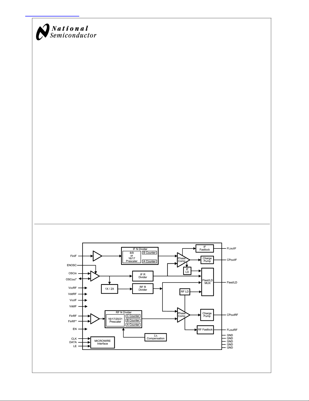
Functional Block Diagram
20072101
© 2003 National Semiconductor Corporation DS200721 www.national.com
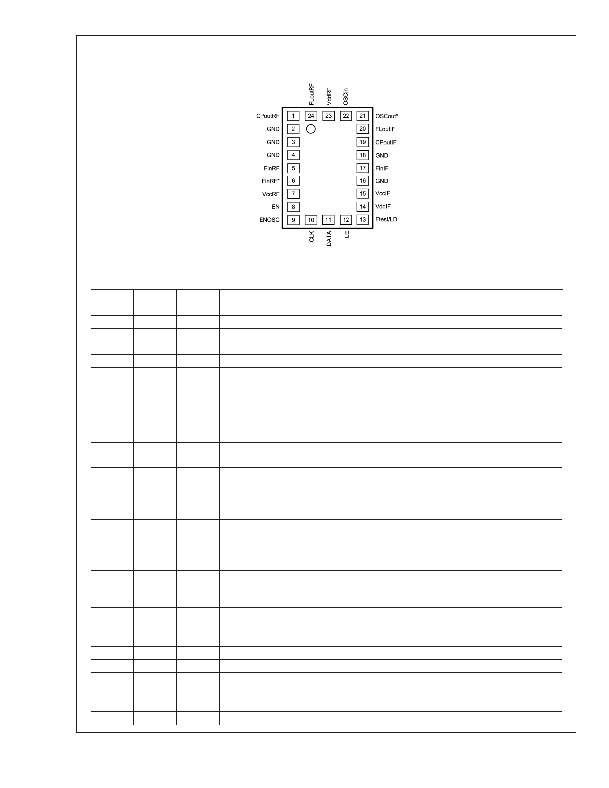
Connection Diagram
LMX2471
Pin Descriptions
Pin # Pin
1 CPoutRF O RF charge pump output.
2 GND - Ground
3 GND - RF Ground
4 GND - Ground for RF PLL digital circuitry.
5 FinRF I RF prescaler input. Small signal input from the VCO.
6 FinRF* I RF prescaler complimentary input. For single-ended operation, a bypass capacitor should
7 VccRF RF PLL power supply voltage input. Must be equal to VccIF . May range from 2.35V to
8 EN I Chip enable input. High impedance CMOS input. When EN is high, the chip is powered
9 ENOSC I This pin should be grounded for normal operation.
10 CLK I MICROWIRE Clock. High impedance CMOS Clock input. Data for the various counters is
11 DATA I MICROWIRE Data. High impedance binary serial data input.
12 LE MICROWIRE Load Enable. High impedance CMOS input. Data stored in the shift
13 Ftest/LD O Test frequency output / Lock Detect
14 VddIF - Digital power supply for IF PLL
15 VccIF - IF power supply voltage input. Must be equal to VccRF. Input may range from 2.35 V to
16 GND - Ground for RF PLL digital circuitry.
17 FinIF I IF prescaler input. Small signal input from the VCO.
18 GND - Digital ground for IF PLL
19 CPoutIF O IF PLL charge pump output
20 FLoutIF O IF Fastlock Output. Also functions as Programmable TRI-STATE CMOS output.
21 OSCout* I/O Complementary reference input or oscillator output.
22 OSCin I Reference input
23 VddRF - Digital power supply for RF PLL
24 FLoutRF O RF Fastlock Output. Also functions as Programmable TRI-STATE CMOS output.
Name
24-Pin CSP (SLE) Package
20072122
I/O Pin Description
be placed as close as possible to this pin and be connected directly to the ground plane.
2.75V. Bypass capacitors should be placed as close as possible to this pin and be
connected directly to the ground plane.
up, otherwise it is powered down.
clocked into the 24 bit shift register on the rising edge.
registers is loaded into the internal latches when LE goes HIGH
2.75 V. Bypass capacitors should be placed as close as possible to this pin and be
connected directly to the ground plane.
www.national.com 2
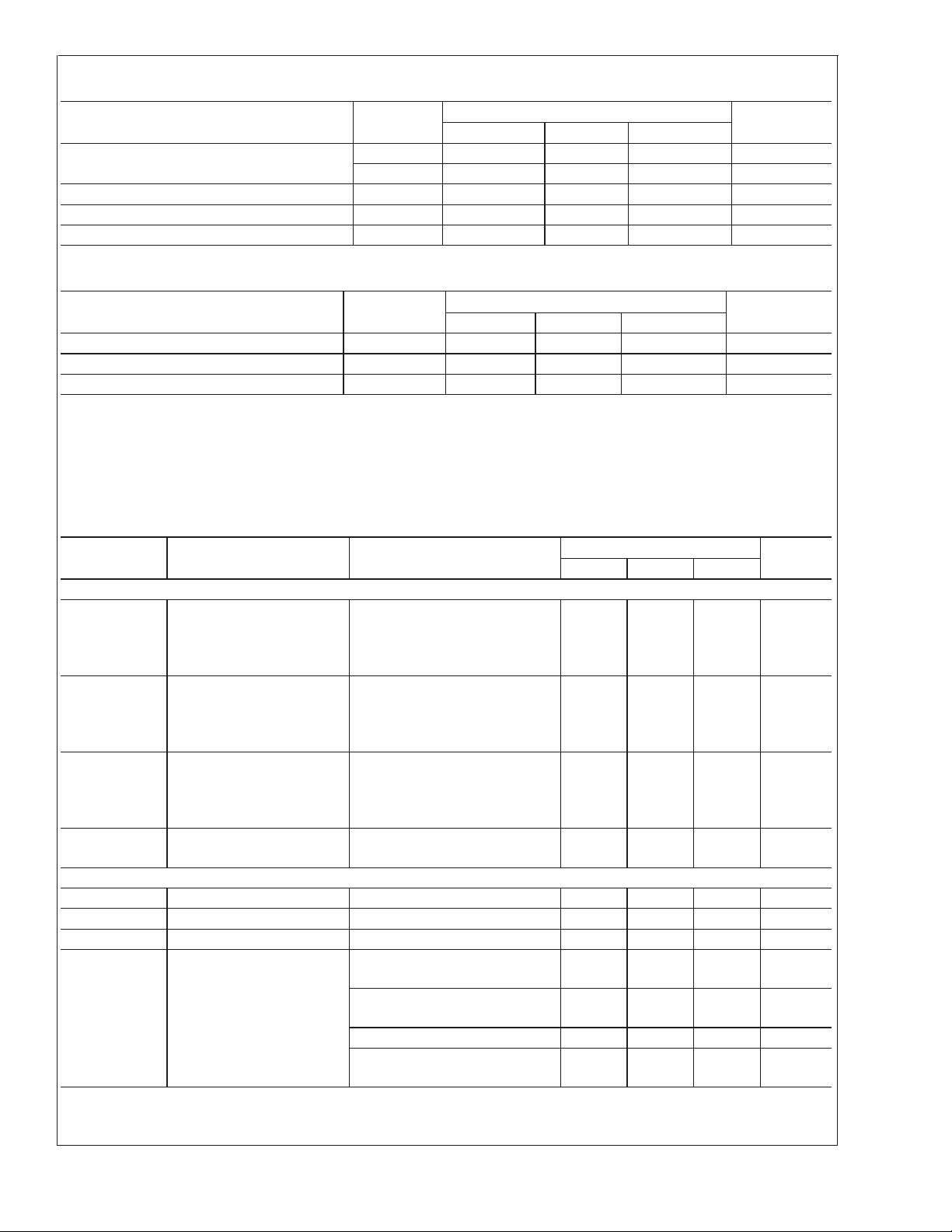
Absolute Maximum Ratings (Notes 1, 2)
LMX2471
Parameter Symbol
Power Supply Voltage V
V
Voltage on any pin with GND =V
=0V V
SS
Storage Temperature Range T
Lead Temperature (Solder 4 sec.) T
Min Typ Max
CC
DD
i
s
L
-0.3 3.0 V
V
CC
-0.3 VCC+ 0.3 V
-65 +150 ˚C
Value
Units
V
CC
+260 ˚C
V
Recommended Operating Conditions
Parameter Symbol
Power Supply Voltage (Note 1) V
Operating Temperature T
Note 1: “Absolute Maximum Ratings” indicate limits beyond which damage to the device may occur. "Recommended Operating Conditions" indicate conditions for
which the device is intended to be functional, but do not guarantee specific performance limits. For guaranteed specifications and test conditions, see the Electrical
Characteristics. The guaranteed specifications apply only for the test conditions listed. Note also that these maximum ratings imply that the voltage at all the power
supply pins of VccRF, VccIF, VddRF, and VddIF are the same. V
Note 2: This Device is a high performance RF integrated circuit with an ESD rating
be done at ESD-free workstations.
Electrical Characteristics (V
CC
V
DD
A
will be used to refer to the voltage at these pins.
CC
= 2.5V; -40˚C ≤ TA≤ +85˚C unless otherwise specified)
CC
Min Typ Max
2.25 2.75 V
V
CC
-40 +85 ˚C
<
2 kV and is ESD sensitive. Handling and assembly of this device should only
Symbol Parameter Conditions
Icc PARAMETERS
I
RF Power Supply Current, RF
CC
Synthesizer
IF PLL OFF
RF PLL ON
Charge Pump TRI-STATE
OSC=0
IF Power Supply Current, IF
I
CC
Synthesizer
IF PLL ON
RF PLL OFF
Charge Pump TRI-STATE
OSC=0
TOTAL Power Supply Current,
I
CC
Entire Synthesizer
IF PLL ON
RF PLL ON
Charge Pump TRI-STATE
OSC=0
PD Power Down Current EN = ENOSC = 0V
I
CC
CLK, DATA, LE = 0V
RF SYNTHESIZER PARAMETERS
f
FinRF
p
FinRF
f
COMP
I
SRCE RF Charge Pump Source
CPoutRF
Operating Frequency 500 3600 MHz
Input Sensitivity -15 0 dBm
Phase Detector Frequency 50 MHz
RF_CPG = 0
Current
V
CPoutRF=VCC
/2
RF_CPG = 1
V
CPoutRF=VCC
/2
... ... µA
RF_CPG = 15
V
CPoutRF=VCC
/2
Value
V
CC
Value
Min Typ Max
3.6 5.7 mA
2.0 2.7 mA
5.6 8.5 mA
115µA
100 µA
200 µA
1600 µA
Units
V
Units
www.national.com3
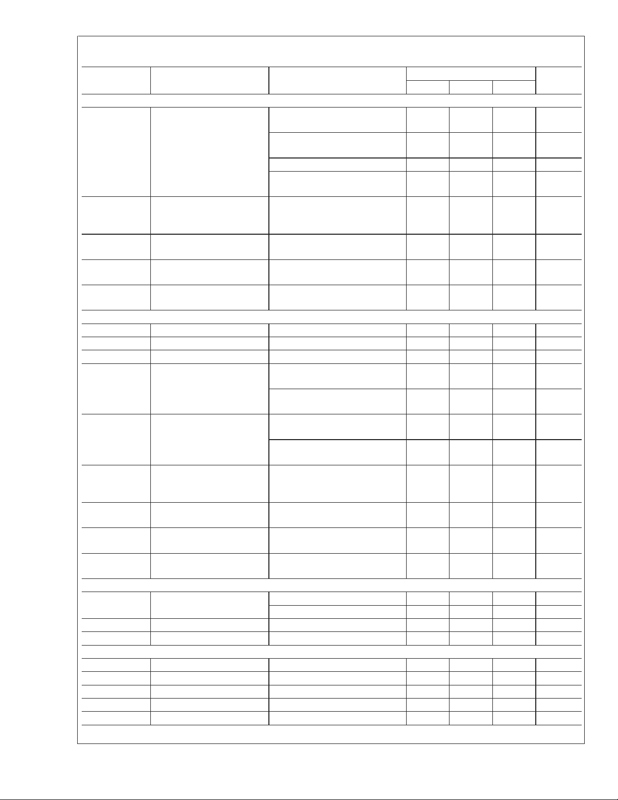
Electrical Characteristics (V
= 2.5V; -40˚C ≤ TA≤ +85˚C unless otherwise specified) (Continued)
CC
LMX2471
Symbol Parameter Conditions
RF SYNTHESIZER PARAMETERS
I
SINK RF Charge Pump Sink
CPoutRF
Current
RF_CPG = 0
V
CPoutRF=VCC
/2
RF_CPG = 1
V
CPoutRF=VCC
/2
... ... µA
RF_CPG = 15
I
TRI RF Charge Pump
CPoutRF
V
CPoutRF=VCC
0.4 ≤ V
CPoutRF
/2
≤ VCC-0.4
TRI-STATE Current
Magnitude
%MIS RF CP Sink vs. CP Source
I
CPoutRF
Mismatch
I
%V RF CP Current vs. CP
CPoutRF
Voltage
I
%TEMP RF CP Current vs.
CPoutRF
V
CPoutRF
= 25˚C
T
A
0.4 ≤ V
= 25˚C
T
A
V
CPoutRF
=VCC/2
CPoutRF
=VCC/2
≤ VCC-0.4
Temperature
IF SYNTHESIZER PARAMETERS
f
FinIF
p
FinIF
f
COMP
I
SRCE IF Charge Pump Source
CPoutIF
Operating Frequency 250 1700 MHz
IF Input Sensitivity -15 0 dBm
Phase Detector Frequency 10 MHz
IF_CPG = 0
Current
V
CPoutIF
=VCC/2
IF_CPG = 1
CPoutIF
CPoutIF
=VCC/2
=VCC/2
I
SINK IF Charge Pump Sink
CPoutIF
Current
V
IF_CPG = 0
V
IF_CPG = 1
CPoutIF
=VCC/2
CPoutIF
≤ VCCRF -0.4
I
TRI IF Charge Pump
CPoutIF
V
0.4 ≤ V
TRI-STATE Current
Magnitude
%MIS IF CP Sink vs. CP Source
I
CPoutIF
Mismatch
I
%V IF CP Current vs. CP
CPoutIF
Voltage
I
%TEMP IF CP Current vs.
CPoutIF
V
CPoutIF
= 25˚C
T
A
0.4 ≤ V
= 25˚C
T
A
V
CPoutIF
=VCC/2
CPoutIF
=VCC/2
≤ VCC-0.4
Temperature
OSCILLATOR PARAMETERS
f
OSCin
v
OSCin
I
OSCin
Oscillator Operating
Frequency
OSC2X = 0 5 110 MHz
OSC2X = 1 5 20 MHz
Oscillator Input Sensitivity 0.5 V
Oscillator Input Current OSC=0 -100 100 µA
DIGITAL INTERFACE (DATA, CLK, LE, EN, ENRF, Ftest/LD, FLoutRF, FLoutIF)
V
IH
V
IL
I
IH
I
IL
V
OH
High-Level Input Voltage 1.6 V
Low-Level Input Voltage 0.4 V
High-Level Input Current VIH=V
CC
Low-Level Input Current VIL= 0 V -1.0 1.0 µA
High-Level Output Voltage IOH= -500 µA VCC-0.4 V
Value
Min Typ Max
Units
-100 µA
-200 µA
-1600 µA
210nA
310%
515%
8%
1mA
4mA
-1 mA
-4 mA
210nA
3%
815%
8%
CC
CC
-1.0 1.0 µA
V
V
www.national.com 4
LMX2471
Electrical Characteristics (V
Symbol Parameter Conditions
= 2.5V; -40˚C ≤ TA≤ +85˚C unless otherwise specified) (Continued)
CC
Value
Min Typ Max
Units
DIGITAL INTERFACE (DATA, CLK, LE, EN, ENRF, Ftest/LD, FLoutRF, FLoutIF)
V
OL
Low-Level Output Voltage IOL= 500 µA 0.4 V
MICROWIRE INTERFACE TIMING
T
CS
T
CH
T
CWH
T
CWL
T
ES
T
EW
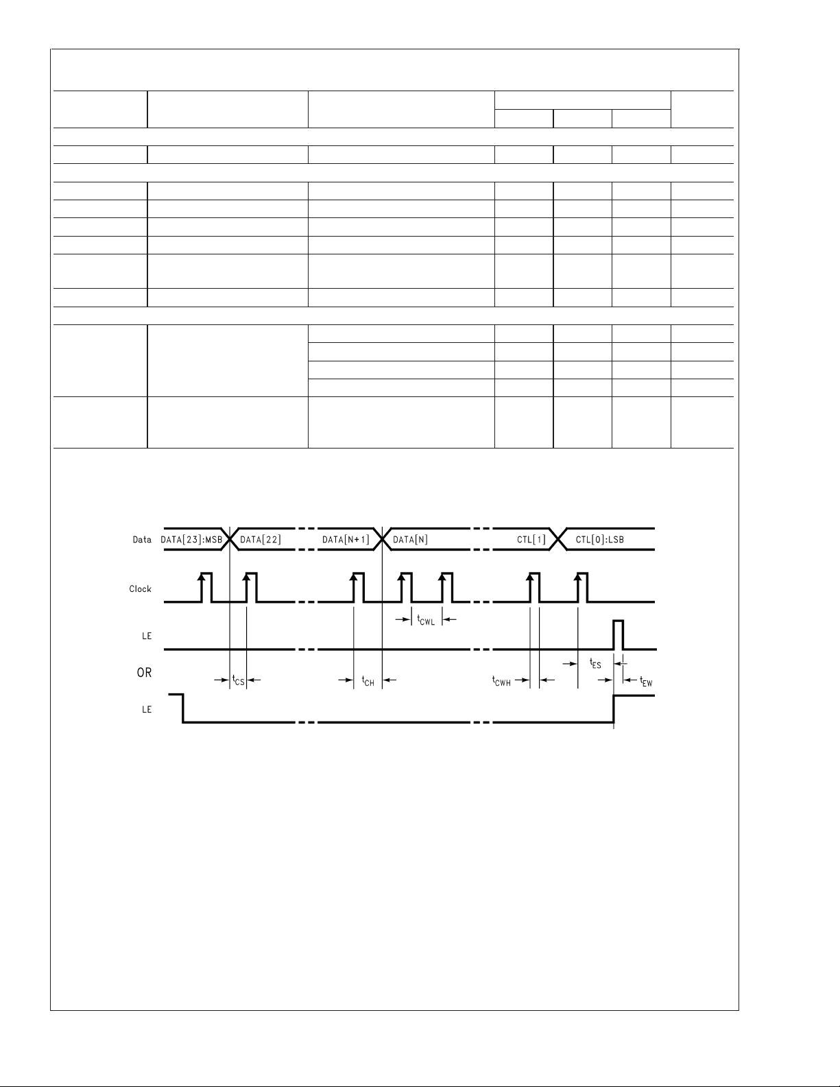
Data to Clock Set Up Time See Microwire Input Timing 50 ns
Data to Clock Hold Time See Microwire Input Timing 10 ns
Clock Pulse Width High See Microwire Input Timing 50 ns
Clock Pulse Width Low See Microwire Input Timing 50 ns
Clock to Load Enable Set
Up Time
See Microwire Input Timing
50 ns
Load Enable Pulse Width See Microwire Input Timing 50 ns
PHASE NOISE
L
RF RF Synthesizer Normalized
F1Hz
Phase Noise Contribution
(Note 3)
RF_CPG = 0 -200 dBc/Hz
RF_CPG = 3 -206 dBc/Hz
RF_CPG = 7 -208 dBc/Hz
RF_CPG = 15 -210 dBc/Hz
L
IF IF Synthesizer Normalized
F1Hz
Phase Noise Contribution
(Note 3)
Note 3: Normalized Phase Noise Contribution is defined as: LN(f) = L(f) – 20log(N) – 10log(f
measured at an offset frequency, f, ina1HzBandwidth. The offset frequency, f, must be chosen sufficiently smaller than the PLL loop bandwidth, yet large enough
to avoid substantial phase noise contribution from the reference source. The offset chosen was 4 KHz.
Applies to both low and high
current modes
OSC=0
-214 dBc/Hz
) where L(f) is defined as the single side band phase noise
COMP
MICROWIRE INPUT TIMING DIAGRAM
20072172
Note 4: Note that although it is valid return the CLK, DATA, and LE pins to a high state after programming is complete, this is not the preferred method. One problem
with keeping these pins at a high voltage is that there is increased leakage through these pins if they are not grounded. Also, the action of returning the CLK pin to
a high voltage after programming is finished can create an extra clock cycle that can cause problems if it is done too soon after the LE pin voltage is returned to a
high state. If possible, it is best to return all microwire pins to 0 V when the PLL is not being programmed in order to avoid these issues with leakage and timing.
www.national.com5
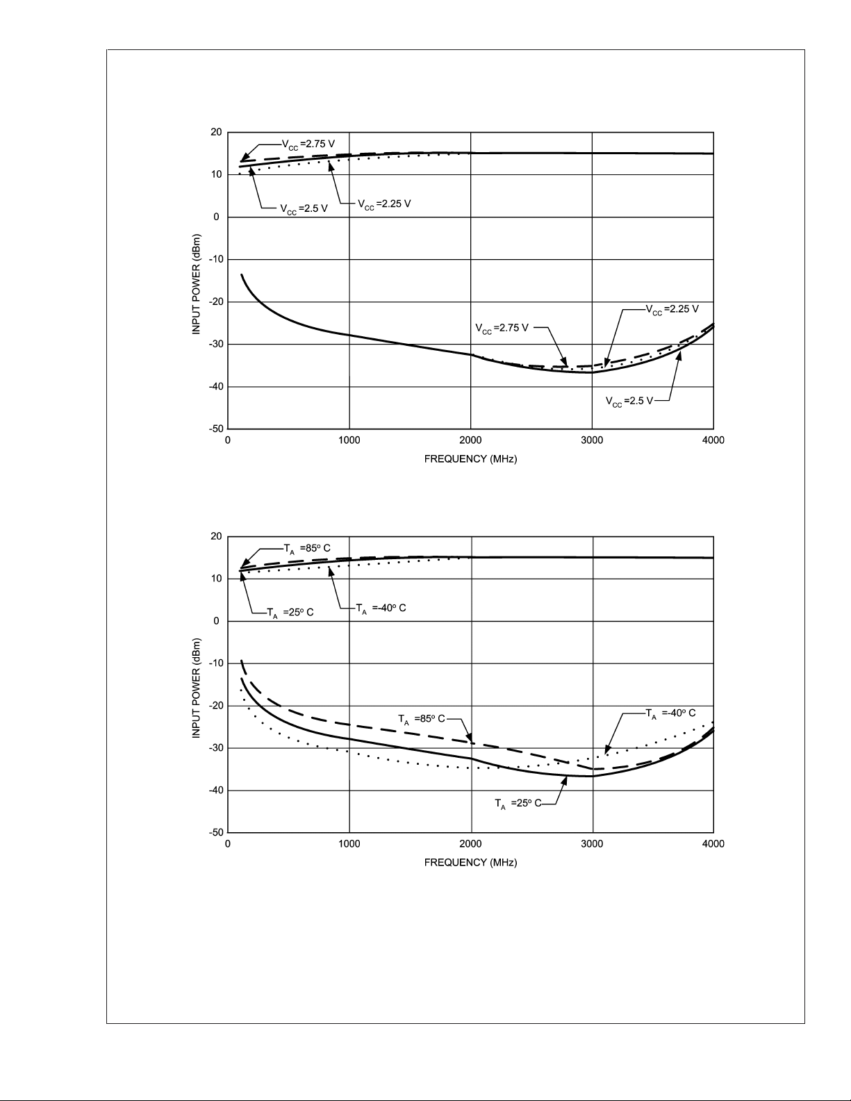
Typical Performance Characteristics : Sensitivity (Note 6)
LMX2471
RF N Counter Sensitivity
= 25˚C
T
A
20072145
RF N Counter Sensitivity
= 2.5 V
V
CC
20072146
www.national.com 6
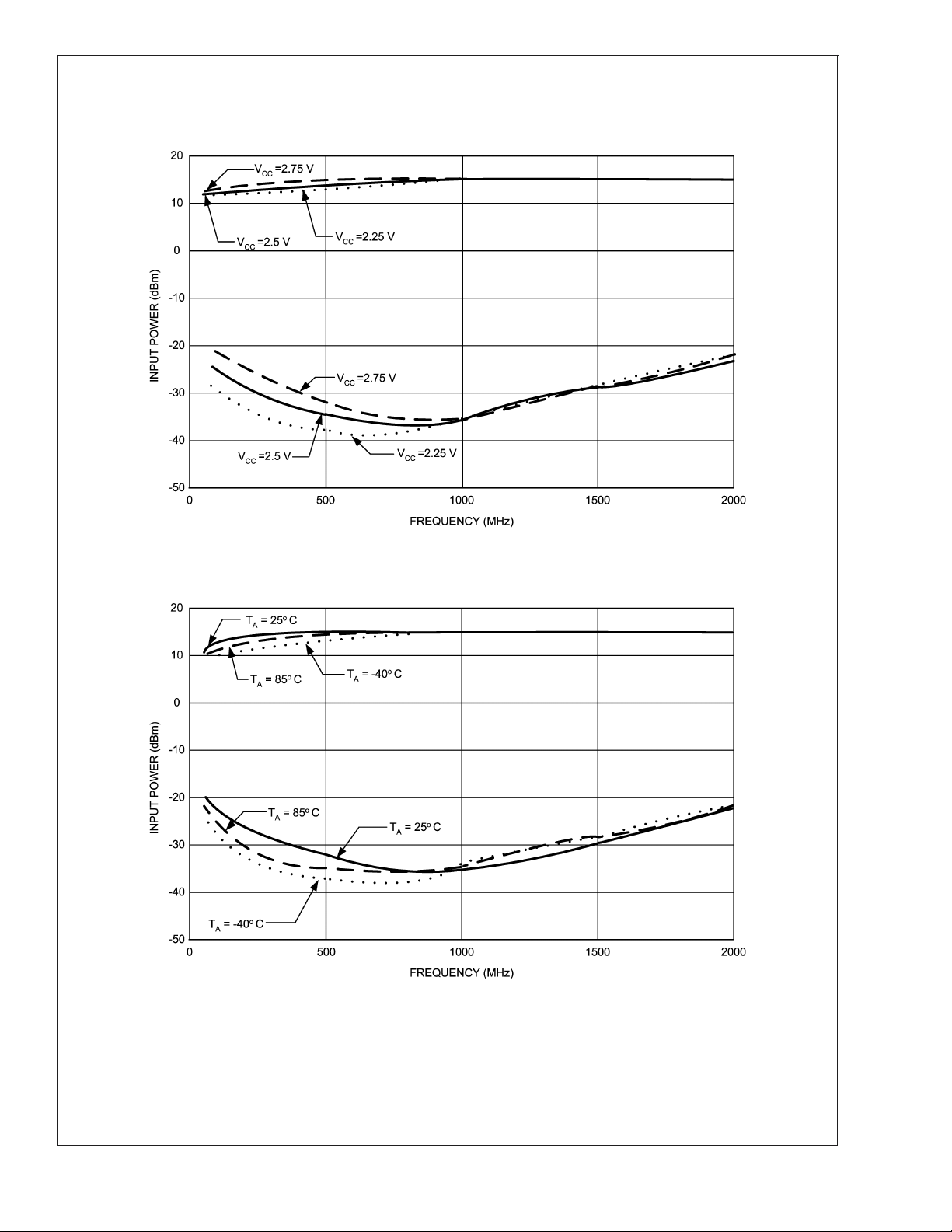
Typical Performance Characteristics : Sensitivity (Note 6) (Continued)
IF N Counter Sensitivity
T
= 25˚C
A
LMX2471
IF N Counter Sensitivity
= 2.5 V
V
CC
20072147
20072148
www.national.com7
Typical Performance Characteristics : Sensitivity (Note 6) (Continued)
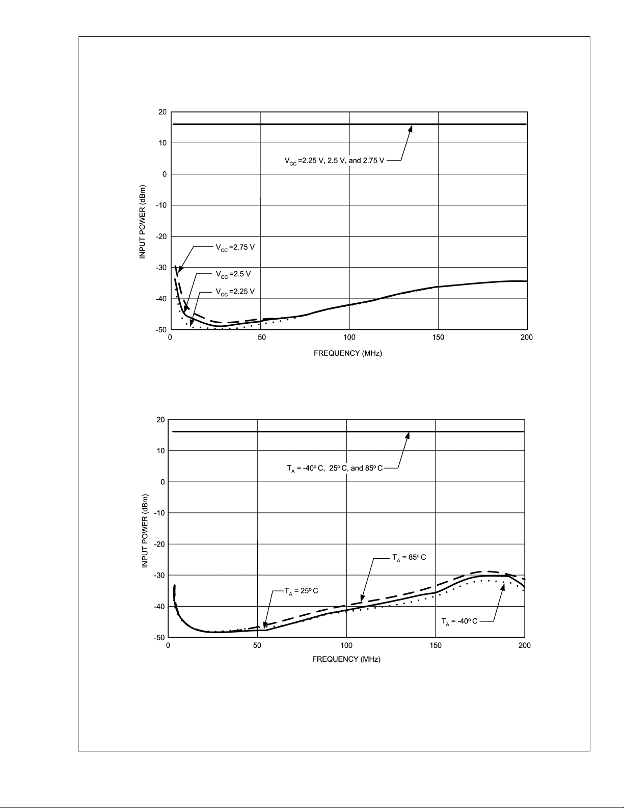
LMX2471
OSCin Counter Sensitivity
OSC=0
= 25˚ C
T
A
20072149
OSCin Counter Sensitivity
OSC=0
= 2.5 V
V
CC
20072150
www.national.com 8
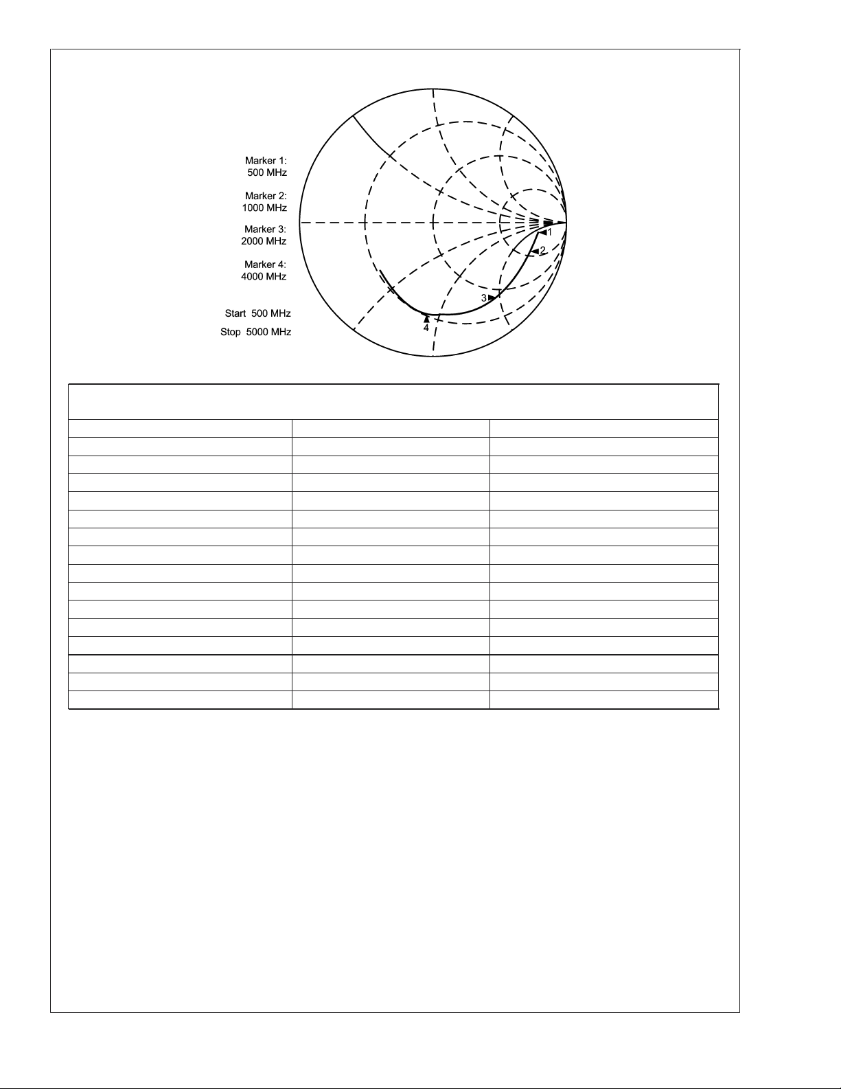
Typical Performance Characteristic : FinRF Input Impedance (Note 6)
20072153
FinRF Input Impedance (VCC=2.5 V, TA=25˚ C)
(Note 5)
Frequency (MHz) Real (Ohms) Imaginary (Ohms)
500 389.9 -158.3
750 270.8 -186.8
1000 160.4 -172.3
1250 95.7 -144.7
1500 61.1 -120.0
1750 44.0 -104.5
2000 36.2 -95.6
2250 32.6 -90.4
2500 32.0 -86.3
2750 30.7 -80.5
3000 28.3 -74.6
3250 26.3 -65.2
3500 22.6 -57.4
3750 18.7 -49.9
4000 16.7 -44.1
LMX2471
www.national.com9
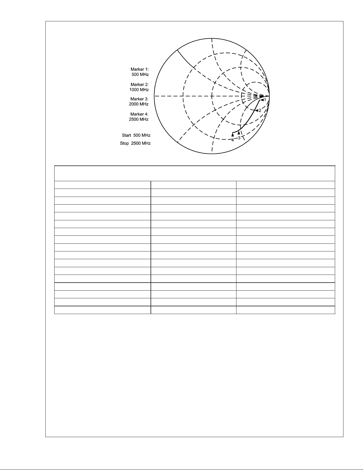
Typical Performance Characteristic : FinIF Input Impedance (Note 6)
LMX2471
20072154
FinIF Input Impedance (VCC=2.5 V, TA=25˚C)
(Note 5)
Freqeuncy (MHz) Real (Ohms) Imaginary (Ohms)
500 377.4 -174.6
600 325.4 -186.6
700 272.7 -192.6
800 222.6 -191.1
900 178.2 -182.4
1000 143.0 -170.6
1100 113.8 -157.1
1200 92.6 -144.5
1300 76.5 -133.0
1400 64.1 -123.0
1500 55.2 -114.9
1600 48.5 -108.2
1700 43.3 -102.9
1800 39.4 -98.4
1900 36.4 -94.6
2000 34.5 -91.6
www.national.com 10
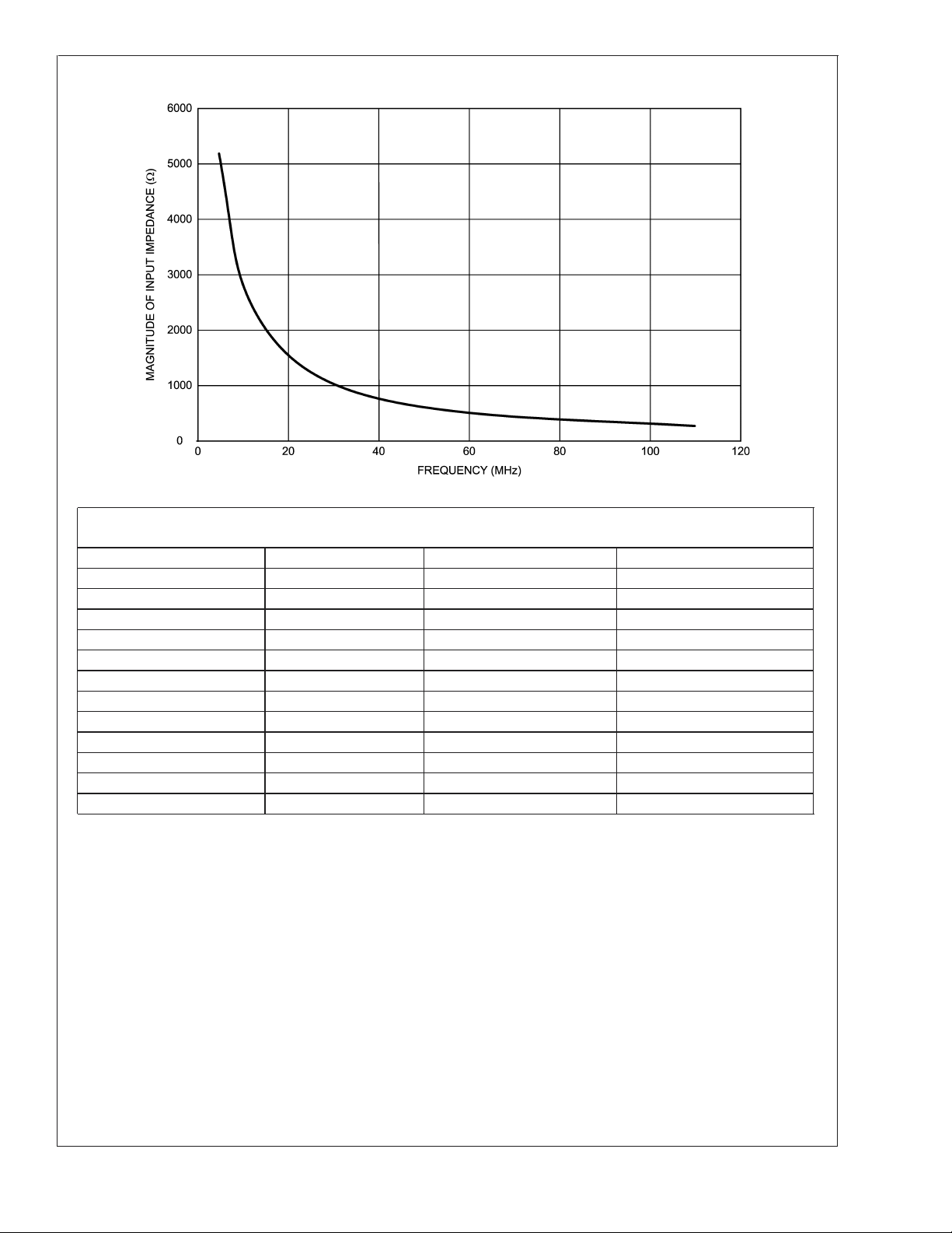
Typical Performance Characteristic : OSCin Input Impedance (Note 6)
20072155
LMX2471
OSCin Input Impedance (VCC=2.5 V, TA=25 ˚C)
(Note 5)
Frequency (MHz) Real (Ohms) Imaginary (Ohms) Magnitude (Ohms)
50 2200 -4700 5189
10 710 -2700 2792
20 229 -1500 1517
30 133 -988 997
40 93 -752 758
50 74 -606 611
60 62 -505 509
70 53 -435 438
80 49 -382 385
90 45 -341 344
100 42 -309 312
110 40 -282 285
www.national.com11
 Loading...