

LMX2430/LMX2433/LMX2434
May 2003
LMX2430/LMX2433/LMX2434 PLLatinum Dual High Frequency Synthesizer for RF Personal
Communications
PLLatinum
™
Dual High Frequency Synthesizer for RF
Personal Communications
LMX2430 3.0 GHz/0.8 GHz
LMX2433 3.6 GHz/1.7 GHz
LMX2434 5.0 GHz/2.5 GHz
General Description
The LMX243x devices are high performance frequency synthesizers with integrated dual modulus prescalers. The
LMX243x devices are designed for use as RF and IF local
oscillators for dual conversion radio transceivers.
A 32/33 or a 16/17 prescale ratio can be selected for the 5.0
GHz LMX2434 RF synthesizer. An 8/9 or a 16/17 prescale
ratio can be selected for both the LMX2430 and LMX2433
RF synthesizers. The IF circuitry contains an 8/9 or a 16/17
prescaler. Using a proprietary digital phase locked loop technique, the LMX243x devices generate very stable, low noise
control signals for RF and IF voltage controlled oscillators.
Both the RF and IF synthesizers include a two-level programmable charge pump. Both the RF and IF synthesizers
have dedicated Fastlock circuitry with integrated timeout
counters. Furthermore, only a single word write is required to
power up and tune the synthesizers to a new frequency.
Serial data is transferred to the devices via a three-wire
interface (DATA, LE, CLK). A low voltage logic interface
allows direct connection to 1.8V devices. Supply voltages
from 2.25V to 2.75V are supported . The LMX243x family
features low current consumption:
LMX2430 (3.0 GHz/ 0.8 GHz) — 2.8 mA/ 1.4 mA, LMX2433
(3.6 GHz/ 1.7 GHz) —3.2 mA/ 2.0 mA, LMX2434 (5.0 GHz/
2.5 GHz) — 4.6 mA/ 2.4 mA at 2.50V.
The LMX243x devices are available in 20-Pin TSSOP and
20-Pin UTCSP surface mount plastic packages.
Features
n Low Current Consumption
n 2.25V to 2.75V Operation
n Selectable Synchronous or Asynchronous Powerdown
Mode
n Selectable Dual Modulus Prescaler:
LMX2430 RF: 8/9 or 16/17
LMX2433 RF: 8/9 or 16/17
LMX2434 RF: 16/17 or 32/33
LMX243x IF: 8/9 or 16/17
n Programmable Charge Pump Current Levels
RF and IF: 1 or 4 mA
n Fastlock
n Digital Filtered Lock Detect Output
n Analog Lock Detect Output (supports both Push-Pull
and Open Drain configurations)
n 1.8V MICROWIRE Logic Interface
n Available in 20-Pin TSSOP and 20-Pin UTCSP
™
Technology with Integrated Timeout Counters
Applications
n Mobile Handsets
(GSM, GPRS, W-CDMA, CDMA, PCS, AMPS, PDC,
DCS)
n Cordless Handsets
(DECT, DCT)
n Wireless Data
n Cable TV Tuners
Thin Shrink Small Outline Package (MTC20) Ultra Thin Chip Scale Package (SLE20A)
20053580
20053581
PLLatinum™is a trademark of National Semiconductor Corporation.
© 2003 National Semiconductor Corporation DS200535 www.national.com
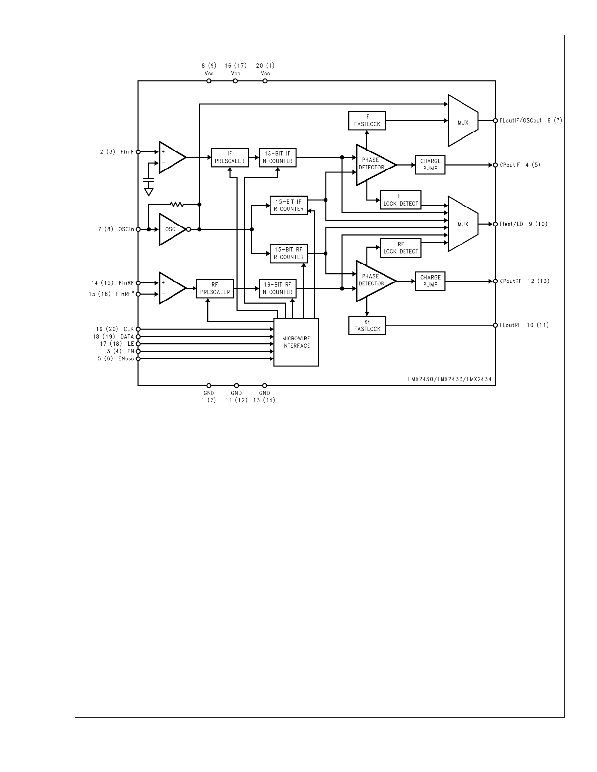
Functional Block Diagram
LMX2430/LMX2433/LMX2434
Note:
1 (2) refers to Pin
#
1 of the 20-Pin UTCSP and Pin#2 of the 20-Pin TSSOP
20053501
www.national.com 2

Connection Diagrams
LMX2430/LMX2433/LMX2434
Ultra Thin Chip Scale Package (SLE)
(Top View)
20053539
Thin Shrink Small Outline Package (TM)
(Top View)
20053583
Pin Descriptions
Pin No.
UTCSP
Pin No.
TSSOP
1 2 GND — Ground for the IF PLL analog and digital circuits, MICROWIRETM, Ftest/LD and
2 3 FinIF I IF PLL prescaler input. Small signal input from the VCO.
3 4 EN I Chip Enable input. High Impedance CMOS input. When this pin is set HIGH,
4 5 CPoutIF O IF PLL charge pump output. The output is connected to the external loop filter,
5 6 ENosc I Oscillator Enable input. High impedance CMOS input. When this pin is set
6 7 OSCout/
7 8 OSCin I Reference oscillator input. The input has an approximate Vcc/2 threshold and is
8 9 Vcc — Power supply bias for the RF PLL digital circuits and oscillator circuits. Vcc may
9 10 Ftest/LD O Programmable multiplexed output. Functions as a general purpose CMOS
Pin Name I/O Description
oscillator circuits.
the RF and IF PLLs are powered up. Powerdown is then controlled through the
MICROWIRE. When this pin is set LOW, the device is asynchronously powered
down and the charge pump output is forced to a high impedance state
(TRI-STATE).
which drives the input of the IF VCO.
HIGH, the oscillator buffer is always powered up, independent of the state of
the EN pin. When this pin is set LOW, the OSCout/ FLoutIF pin functions as an
IF Fastlock output, which connects a resistor in parallel to R2 of the external
loop filter.
O Oscillator output/ IF PLL Fastlock output. The output configuration is dependent
FLoutIF
on the state of the ENosc pin. When ENosc is set LOW, the pin functions as an
IF Fastlock output, which connects a resistor in parallel to R2 of the external
loop filter. This configuration also functions as a general purpose CMOS
TRI-STATE output. When ENosc is set HIGH, the pin functions as an oscillator
output so that an external crystal can be used.
driven by an external AC coupled source.
range from 2.25V to 2.75V. Bypass capacitors should be placed as close as
possible to this pin and be connected directly to the ground plane.
TRI-STATE output, N and R divider output, RF/ IF PLL push-pull analog lock
detect output, RF/ IF PLL open-drain analog lock detect output, or RF/ IF PLL
digital filtered lock detect output.
www.national.com3

Pin Descriptions (Continued)
Pin No.
UTCSP
10 11 FLoutRF O RF PLL Fastlock output. This pin connects a resistor in parallel to R2 of the
11 12 GND — Ground for the RF PLL digital circuits.
12 13 CPoutRF O RF PLL charge pump output. The output is connected to the external loop filter,
LMX2430/LMX2433/LMX2434
13 14 GND — Ground for the RF PLL analog circuits.
14 15 FinRF I RF PLL prescaler input. Small signal input from the VCO.
15 16 FinRF
16 17 Vcc — Power supply bias for the RF PLL analog circuits. Vcc may range from 2.25V to
17 18 LE I MICROWIRE Latch Enable input. High impedance CMOS input. When LE
18 19 CLK I MICROWIRE Clock input. High impedance CMOS input. DATA is clocked into
19 20 DATA I MICROWIRE Data input. High impedance CMOS input. Binary serial data. The
20 1 Vcc — Power supply bias for the IF PLL analog and digital circuits, MICROWIRE, and
Pin No.
TSSOP
Pin Name I/O Description
external loop filter. This pin can also function as a general purpose CMOS
TRI-STATE output.
which drives the input of the RF VCO.
*
I RF PLL prescaler complementary input. For single ended operation, this pin
should be AC grounded through a 100 pF capacitor. The LMX243x can be
driven differentially when the AC coupled capacitor is omitted.
2.75V. Bypass capacitors should be placed as close as possible to this pin and
be connected directly to the ground plane.
transitions HIGH, DATA stored in the shift register is loaded into one of 6
internal control registers.
the 24-bit shift register on the rising edge of CLK.
MSB of DATA is shifted in first. The two last bits are the control bits.
Ftest/LD circuits. Vcc may range from 2.25V to 2.75V. Bypass capacitors
should be placed as close as possible to this pin and be connected directly to
the ground plane
www.national.com 4

Ordering Information
Model Temperature Range Package Description Packing NS Package Number
LMX2430TM -40˚C to +85˚C Thin Shrink Small
LMX2430TMX -40˚C to +85˚C Thin Shrink Small
LMX2430SLEX -40˚C to +85˚C Ultra Thin Chip Scale
LMX2433TM -40˚C to +85˚C Thin Shrink Small
LMX2433TMX -40˚C to +85˚C Thin Shrink Small
LMX2433SLEX -40˚C to +85˚C Ultra Thin Chip Scale
LMX2434TM -40˚C to +85˚C Thin Shrink Small
LMX2434TMX -40˚C to +85˚C Thin Shrink Small
LMX2434SLEX -40˚C to +85˚C Ultra Thin Chip Scale
LMX2430/LMX2433/LMX2434
73 Units Per Rail MTC20
Outline Package
(TSSOP)
2500 Units Per Reel MTC20
Outline Package
(TSSOP)
Tape and Reel
2500 Units Per Reel SLE20A
Package (UTCSP)
Tape and Reel
73 Units Per Rail MTC20
Outline Package
(TSSOP)
2500 Units Per Reel MTC20
Outline Package
(TSSOP)
Tape and Reel
2500 Units Per Reel SLE20A
Package (UTCSP)
Tape and Reel
73 Units Per Rail MTC20
Outline Package
(TSSOP)
2500 Units Per Reel MTC20
Outline Package
(TSSOP)
Tape and Reel
2500 Units Per Reel SLE20A
Package (UTCSP)
Tape and Reel
www.national.com5

Absolute Maximum Ratings (Notes 1,
2, 3)
If Military/Aerospace specified devices are required,
please contact the National Semiconductor Sales Office/
Distributors for availability and specifications.
Power Supply Voltage
Vcc to GND −0.3V to +3.25V
Voltage on any pin to GND (V
V
must be<+3.25V −0.3V to Vcc+0.3V
I
LMX2430/LMX2433/LMX2434
Storage Temperature Range (T
Lead Temperature (solder 4 s) (T
)
I
) −65˚C to +150˚C
S
) +260˚C
L
Electrical Characteristics
Vcc = EN = 2.5V, −40˚C ≤ TA≤ +85˚C, unless otherwise specified
Symbol Parameter Conditions
I
PARAMETERS
CC
Icc
RF
Icc
IF
Icc
PD
RF SYNTHESIZER PARAMETERS
f
FinRF
N
RF
R
RF
f
COMPRF
p
FinRF
Power Supply
Current, RF
Synthesizer
Power Supply
Current, IF
Synthesizer
LMX2430 CLK, DATA and LE = 0V
OSCin = GND
LMX2433 3.2 4.4 mA
LMX2434 4.6 6.2 mA
RF_PD Bit = 0
IF_PD Bit = 1
RF_P Bit = 0
LMX2430 CLK, DATA and LE = 0V
OSCin = GND
LMX2433 2.0 2.8 mA
LMX2434 2.4 3.5 mA
RF_PD Bit = 1
IF_PD Bit = 0
IF_P Bit = 0
Powerdown Current EN, ENosc, CLK, DATA
and LE = 0V
RF Operating
Frequency
LMX2430 RF_P Bit = 0 250 2500 MHz
RF_P Bit = 1 250 3000 MHz
LMX2433 RF_P Bit = 0 500 3000 MHz
RF_P Bit = 1 500 3600 MHz
LMX2434 RF_P Bit = 0 or 1 1000 5000 MHz
N Divider Range P = 8/9
(Note 4)
P = 16/17
(Note 4)
P = 32/33
(Note 4)
RF R Divider Range 3 32767
RF Phase Detector Frequency 10 MHz
RF Input Sensitivity LMX2430/33
2.25V ≤ Vcc ≤ 2.75V
(Note 5)
LMX2434
2.35V ≤ Vcc ≤ 2.75V
(Note 5)
Recommended Operating Conditions
Power Supply Voltage
Vcc to GND +2.25V to +2.75V
Operating Temperature (T
Note 1: Absolute Maximum Ratings indicate limits beyond which damage to
the device may occur. Recommended Operating Conditions indicate conditions for which the device is intended to be functional, but do not guarantee
specific performance limits. For guaranteed specifications and test conditions, refer to the Electrical Characteristics section. The guaranteed specifications apply only for the conditions listed.
Note 2: This device is a high performance RF integrated circuit with an ESD
<
rating
2 kV and is ESD sensitive. Handling and assembly of this device
should only be done at ESD protected work stations.
Note 3: GND=0V
(Note 1)
) −40˚C to +85˚C
A
Value
Min Typ Max
2.8 3.6 mA
1.4 2.0 mA
24 262151
48 524287
96 524287
−15 0 dBm
−12 0 dBm
Units
10 µA
www.national.com 6

Electrical Characteristics (Continued)
Vcc = EN = 2.5V, −40˚C ≤ TA≤ +85˚C, unless otherwise specified
Symbol Parameter Conditions
RF SYNTHESIZER PARAMETERS
I
CPoutRF
Source
I
CPoutRF
Sink
I
CPoutRF
TRI
I
CPoutRF
%MIS
I
CPoutRF
%V
CPoutRF
I
CPoutRF
%T
A
IF SYNTHESIZER PARAMETERS
f
FinIF
N
IF
R
IF
f
COMPIF
p
FinIF
I
CPoutIF
Source
I
CPoutIF
Sink
RF Charge Pump Output Source
Current
V
CPoutRF
= Vcc/2
RF_CPG Bit = 0
(Note 6)
CPoutRF
= Vcc/2
V
RF_CPG Bit = 1
(Note 6)
RF Charge Pump Output Sink Current V
CPoutRF
= Vcc/2
RF_CPG Bit = 0
(Note 6)
CPoutRF
= Vcc/2
V
RF_CPG Bit = 1
(Note 6)
RF Charge Pump Output TRI-STATE
Current
RF Charge Pump Output Sink Current
Vs Charge Pump Output Source
0.5V ≤ V
(Note 6)
V
CPoutRF
(Note 7)
CPoutRF
= Vcc/2
≤ Vcc - 0.5V
Current Mismatch
RF Charge Pump Output Current
Magnitude Variation Vs Charge Pump
0.5V ≤ V
(Note 7)
CPoutRF
≤ Vcc - 0.5V
Output Voltage
RF Charge Pump Output Current
Magnitude Variation Vs Temperature
IF Operating
Frequency
LMX2430 IF_P Bit = 0 or 1 100 800 MHz
LMX2433 IF_P Bit = 0 or 1 250 1700 MHz
V
CPoutRF
(Note 7)
= Vcc/2
LMX2434 IF_P Bit = 0 or 1 500 2500 MHz
IF N Divider Range P = 8/9
(Note 4)
P = 16/17
(Note 4)
IF R Divider Range 3 32767
IF Phase Detector Frequency 10 MHz
IF Input Sensitivity 2.25V ≤ Vcc ≤ 2.75V
(Note 5)
IF Charge Pump Output Source
Current
V
CPoutIF
= Vcc/2
IF_CPG Bit = 0
(Note 6)
CPoutIF
= Vcc/2
V
IF_CPG Bit = 1
(Note 6)
IF Charge Pump Output Sink Current V
CPoutIF
= Vcc/2
IF_CPG Bit = 0
(Note 6)
CPoutIF
= Vcc/2
V
IF_CPG Bit = 1
(Note 6)
Value
Min Typ Max
Units
-1.0 mA
-4.0 mA
1.0 mA
4.0 mA
-2.5 2.5 nA
310%
515%
2%
24 131079
48 262143
-15 0 dBm
-1.0 mA
-4.0 mA
1.0 mA
4.0 mA
LMX2430/LMX2433/LMX2434
www.national.com7

Electrical Characteristics (Continued)
Vcc = EN = 2.5V, −40˚C ≤ TA≤ +85˚C, unless otherwise specified
Symbol Parameter Conditions
IF SYNTHESIZER PARAMETERS
I
CPoutIF
TRI
I
CPoutIF
%MIS
LMX2430/LMX2433/LMX2434
I
CPoutIF
%V
CPoutIF
I
CPoutIF
%T
A
OSCILLATOR PARAMETERS
f
OSCin
v
OSCin
I
OSCin
DIGITAL INTERFACE (DATA, CLK, LE, EN, ENosc, Ftest/LD, FLoutRF, OSCout/ FLoutIF)
V
IH
V
IL
I
IH
I
IL
V
OH
V
OL
MICROWIRE INTERFACE
t
CS
t
CH
t
CWH
t
CWL
t
ES
t
EW
IF Charge Pump Output TRI-STATE
Current
IF Charge Pump Output Sink Current
Vs Charge Pump Output Source
0.5V ≤ V
(Note 6)
V
CPoutIF
(Note 7)
CPoutIF
= Vcc/2
≤ Vcc - 0.5V
Current Mismatch
IF Charge Pump Output Current
Magnitude Variation Vs Charge Pump
0.5V ≤ V
(Note 7)
CPoutIF
≤ Vcc - 0.5V
Output Voltage
IF Charge Pump Output Current
Magnitude Variation Vs Temperature
V
CPoutIF
(Note 7)
= Vcc/2
Oscillator Operating Frequency 1 256 MHz
Oscillator Sensitivity (Note 8) 0.5 Vcc V
Oscillator Input Current V
= Vcc 100 µA
OSCin
V
= 0V -100 µA
OSCin
High-Level Input Voltage 1.6 V
Low-Level Input Voltage 0.4 V
High-Level Input Current VIH= Vcc 1.0 µA
Low-Level Input Current VIL= 0V −1.0 µA
High-Level Output Voltage IOH= −500 µA VCC−
Low-Level Output Voltage IOL= 500 µA 0.4 V
DATA to CLK Set Up Time (Note 9) 50 ns
DATA to CLK Hold Time (Note 9) 10 ns
CLK Pulse Width HIGH (Note 9) 50 ns
CLK Pulse Width LOW (Note 9) 50 ns
CLK to LE Set Up Time (Note 9) 50 ns
LE Pulse Width (Note 9) 50 ns
Value
Min Typ Max
Units
-2.5 2.5 nA
310%
515%
2%
0.4
PP
V
www.national.com 8

Electrical Characteristics (Continued)
Vcc = EN = 2.5V, −40˚C ≤ TA≤ +85˚C, unless otherwise specified
Symbol Parameter Conditions
PHASE NOISE CHARACTERISTICS
L
(f) RF Synthesizer Normalized Phase
NRF
Noise Contribution
(Note 10)
(f) IF Synthesizer Normalized Phase
L
NIF
Noise Contribution
(Note 10)
(f) RF Synthesizer Single
L
RF
Side Band Phase
Noise Measured
LMX2430 f
LMX2433 f
LMX2434 f
TCXO Reference Source
RF_CPG Bit = 1
IF_PD Bit = 1
TCXO Reference Source
IF_CPG Bit = 1
RF_PD Bit = 1
= 2750 MHz
FinRF
f = 10 kHz offset
f
COMPRF
= 1 MHz
Loop Bandwidth = 100 kHz
= 2750
N
RF
=10MHz
f
OSCin
=1V
v
OSCin
PP
RF_CPG Bit = 1
IF_PD Bit = 1
= +25oC
T
A
(Note 11)
= 3200 MHz
FinRF
f = 10 kHz offset
f
COMPRF
= 1 MHz
Loop Bandwidth = 100 kHz
= 3200
N
RF
=10MHz
f
OSCin
=1V
v
OSCin
PP
RF_CPG Bit = 1
IF_PD Bit = 1
= +25oC
T
A
(Note 11)
= 4700 MHz
FinRF
f = 10 kHz offset
f
COMPRF
= 1 MHz
Loop Bandwidth = 100 kHz
= 4700
N
RF
=10MHz
f
OSCin
=1V
v
OSCin
PP
RF_CPG Bit = 1
IF_PD Bit = 1
= +25oC
T
A
(Note 11)
Value
Min Typ Max
-219.0 dBc/
-214.0 dBc/
-90.30 dBc/
-88.90 dBc/
-85.60 dBc/
LMX2430/LMX2433/LMX2434
Units
Hz
Hz
Hz
Hz
Hz
Note 4: Some of the values in this range are illegal divide ratios (B<A). To obtain continuous legal division, the Minimum Divide Ratio must be calculated. Use N
*
≥ P
(P−1), where P is the value of the prescaler selected.
Note 5: Refer to the LMX243x FinRF Sensitivity Test Setup section
Note 6: Refer to the LMX243x Charge Pump Test Setup section
Note 7: Refer to the Charge Pump Current Specification Definitions for details on how these measurements are made.
Note 8: Refer to the LMX243x OSCin Sensitivity Test Setup section
Note 9: Refer to the LMX243x Serial Data Input Timing section
Note 10: Normalized Phase Noise Contribution is defined as : L
measured at an offset frequency, f, ina1Hzbandwidth. The offset frequency, f, must be chosen sufficiently smaller than the PLL’s loop bandwidth, yet large enough
to avoid substantial phase noise contribution from the reference source. N is the value selected for the feedback divider and f
detector comparison frequency.
Note 11: The synthesizer phase noise is measured with the LMX2430TM/LMX2430SLE Evaluation boards and the HP8566B Spectrum Analyzer.
(f) = L(f) − 20 log (N) − 10 log (f
N
), where L(f) is defined as the single side band phase noise
COMP
is the RF/IF phase/ frequency
COMP
www.national.com9
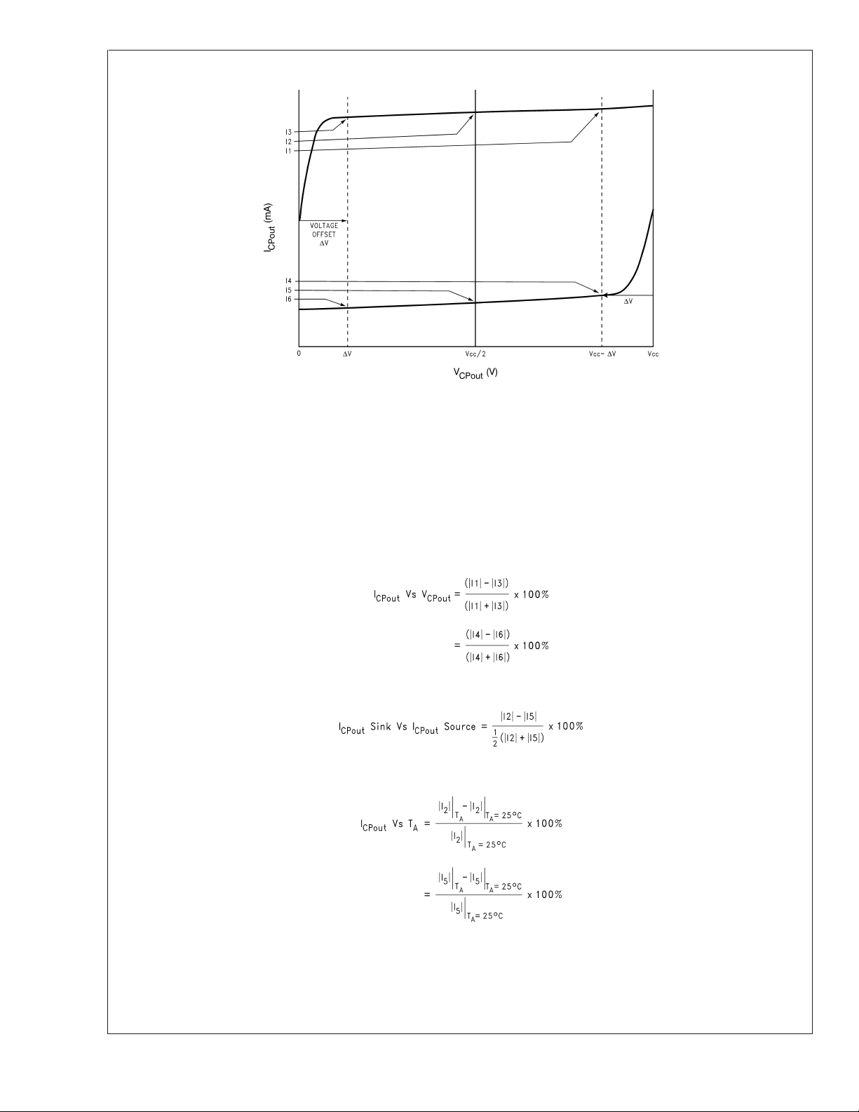
Charge Pump Current Specification Definitions
LMX2430/LMX2433/LMX2434
I1 = Charge Pump Sink Current at V
I2 = Charge Pump Sink Current at V
I3 = Charge Pump Sink Current at V
I4 = Charge Pump Source Current at V
I5 = Charge Pump Source Current at V
I6 = Charge Pump Source Current at V
CPout
CPout
CPout
CPout
CPout
CPout
= Vcc − ∆V
= Vcc//2
= ∆V
= Vcc − ∆V
= Vcc/2
= ∆V
20053537
∆V = Voltage offset from the positive and negative rails. Dependent on the VCO tuning range relative to Vcc and GND. Typical values are between 0.5V and
1.0V.
V
CPout
I
refers to either I
CPout
refers to either V
CPoutRF
CPoutRF
or I
or V
CPoutIF
CPoutIF
Charge Pump Output Current Magnitude Variation Vs Charge Pump Output Voltage
20053563
Charge Pump Output Sink Current Vs Charge Pump Output Source Current Mismatch
20053564
Charge Pump Output Current Magnitude Variation Vs Temperature
www.national.com 10
20053565
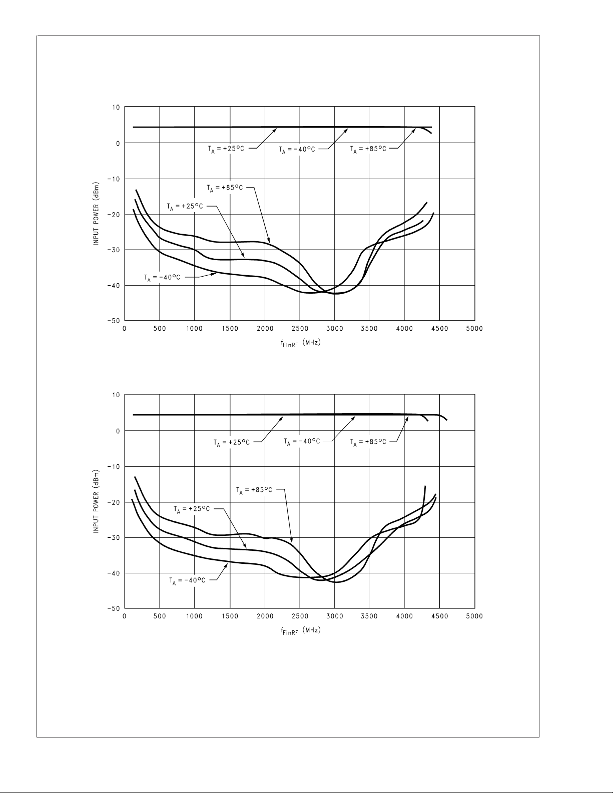
Typical Performance Characteristics Sensitivity
LMX2430 FinRF Input Power Vs Frequency
Vcc = EN = 2.25V
LMX2430/LMX2433/LMX2434
LMX2430 FinRF Input Power Vs Frequency
Vcc = EN = 2.75V
20053592
20053593
www.national.com11

Typical Performance Characteristics
Sensitivity
LMX2430/LMX2433/LMX2434
(Continued)
LMX2433 FinRF Input Power Vs Frequency
Vcc = EN = 2.25V
LMX2433 FinRF Input Power Vs Frequency
Vcc = EN = 2.75V
20053594
20053595
www.national.com 12
Typical Performance Characteristics
Sensitivity
(Continued)
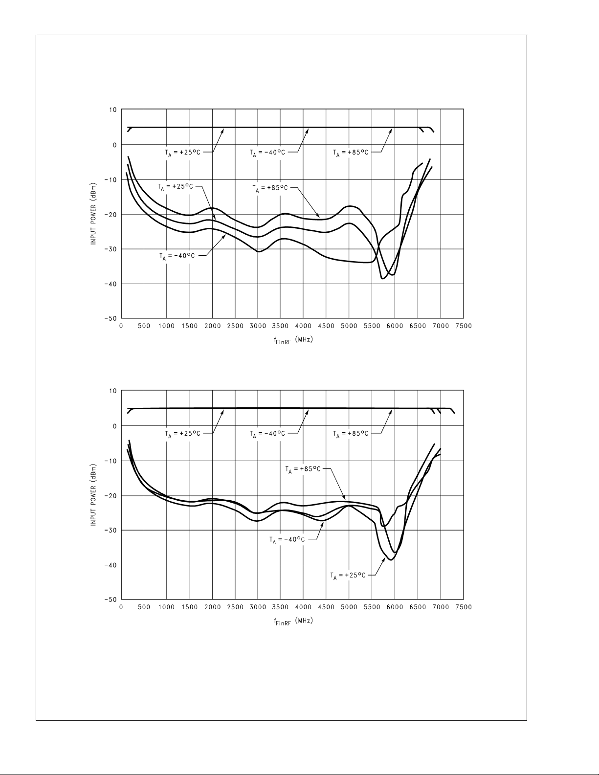
LMX2434 FinRF Input Power Vs Frequency
Vcc = EN = 2.35V
LMX2430/LMX2433/LMX2434
LMX2434 FinRF Input Power Vs Frequency
Vcc = EN = 2.75V
20053596
20053597
www.national.com13

Typical Performance Characteristics
Sensitivity
LMX2430/LMX2433/LMX2434
(Continued)
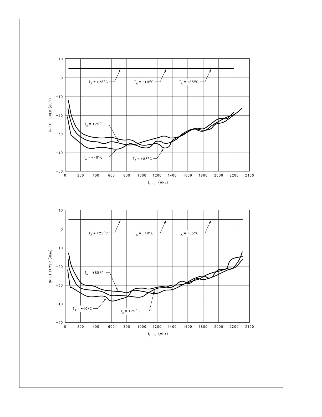
LMX2430 FinIF Input Power Vs Frequency
Vcc = EN = 2.25V
LMX2430 FinIF Input Power Vs Frequency
Vcc = EN = 2.75V
20053598
20053599
www.national.com 14
Typical Performance Characteristics
Sensitivity
(Continued)
LMX2433 FinIF Input Power Vs Frequency
Vcc = EN = 2.25V
LMX2430/LMX2433/LMX2434
LMX2433 FinIF Input Power Vs Frequency
Vcc = EN = 2.75V
200535A0
200535A1
www.national.com15
 Loading...