


查询LMX2364供应商
LMX2364
2.6 GHz PLLatinum Fractional RF Frequency Synthesizer
with 850 MHz Integer IF Frequency Synthesizer
General Description
The LMX2364 integrates a high performance 2.6 GHz fractional frequency synthesizer with a 850 MHz low power
Integer-N frequency synthesizer. Designed for use in a local
oscillator subsystem of a radio transceiver, the LMX2364
generates very stable, low noise control signals for UHF and
VHF voltage controlled oscillators. It is fabricated using National’s high performance BiCMOS process.
The RF Synthesizer supports both fractional and integer
modes. The N counter contains a selectable, quadruple
modulus prescaler and can support fractional denominators
from 1 to 128. A flexible, 4 level programmable charge pump
supplies output current magnitudes ranging from 1 mA to 16
mA. Only a single word write is required to power up and
tune the synthesizer to a new frequency.
™
High performance FastLock
LMX2364 an excellent choice for applications requiring aggressive lock time while maintaining excellent phase noise
and spurious performance. The combination of the improved
FastLock circuitry, the enhanced fractional compensation
engine, and the programmable charge pump architecture
gives the designer maximum freedom to optimize the performance of the synthesizer for the target application. Integrated timeout counters greatly simplify the programming
aspects of FastLock. These timeout counters reduce the
demands on the microcontroller by automatically disengaging FastLock after a perscribed number of reference cycles
of the phase detector.
The IF synthesizer includes a fixed 8/9 dual modulus prescaler, a two level programmable charge pump, and dedicated FastLock circuitry with an integrated timeout counter.
The LMX2364 offers many performance enhancements over
the LMX2354. Improvements in the fractional compensation
make the spurs on the LMX2364 approximately 6 dB better
in a typical application. The higher and more flexible fractional modulus combined with the higher charge pump currents result in phase noise improvements on the order of 10
dB. The cycle slip reduction circuitry of the LMX2364 is both
easy to use and effective in reducing cycle slipping and
allows one to use very high phase detector frequencies
without degrading lock times.
Serial data is transferred to the device via a three-wire
interface (DATA, LE, CLK). The low voltage logic interface
technology makes the
allows direct connection to 1.8 Volt and 3.0 Volt devices.
Supply voltages from 2.7V to 5.5V are supported. Independent charge pump supplies for each synthesizer allows the
designer to optimize the bias level for the selected VCO. The
LMX2364 consumes 5.0 mA (typical) of current in integer
mode and 7.2 mA (typical) in fractional mode. The LMX2364
is available in a 24 Pin Ultra Thin CSP package and 24 Pin
TSSOP Package.
Features
n RF Synthesizer supports both Fractional and Integer
Operating Modes
n Pin Compatible upgrade for LMX2354
n 2.7V to 5.5V operation
n Pin and programmable power down
n Fractional N divider supports fractional denominators
ranging from 1 through 128
n Supports Integer Mode Operation
n Programmable charge pump current levels
RF: 4 level, 1 – 16 mA
IF: 2 level, 100/800 uA
n FastLock Technology with integrated timeout counters
n Digital filtered & analog lock detect output
n FastLock Glitch Reduction Technology
n Enhanced Low Noise Fractional Compensation Engine
n Low voltage programming interface allows direct
connection to 1.8V logic
Applications
n Digital Cellular
n GPRS
n IS-136
n GAIT
n PDC
n EDGE
n CDMA
n Zero blind slot TDMA systems
n Cable TV Tuners (CATV)
July 2003
LMX2364 2.6 GHz PLLatinum Fractional RF Frequency Synthesizer with 850 MHz Integer-N IF
Frequency Synthesizer
FastLock™is a trademark of National Semiconductor Corporation.
®
TRI-STATE
© 2003 National Semiconductor Corporation DS200506 www.national.com
is a registered trademark of National Semiconductor Corporation.

Functional Block Diagram
LMX2364
Connection Diagrams
24-Pin TSSOP (TM) Package Ultra Thin 24-Pin CSP (SLE) Package
20050601
20050602
www.national.com 2
20050622

Pin Descriptions
LMX2364
Pin Number
TSSOP SLE
2 1 VccRF RF PLL power supply voltage input. Must be equal to V
Pin Description
. May range from 2.7V to
VccIF
5.5V. Bypass capacitors should be placed as close as possible to this pin and be
connected directly to the ground plane.
3 2 VcpRF Power supply for RF charge pump. Must be ≥ V
VccRF
and V
VccIF
.
4 3 CPoutRF RF charge pump output.
5 4 GND Ground for RF PLL digital circuitry.
6 5 FinRF RF prescaler input. Small signal input from the VCO.
7 6 FinRF* RF prescaler complementary input. For single-ended operation, a bypass capacitor
should be placed as close as possible to this pin and be connected directly to the
ground plane.
8 7 GND Ground for RF PLL analog circuitry.
9 8 OSCinRF RF R counter input. Has a V
/2 input threshold when configured as an input and can
CC
be driven from an external CMOS or TTL logic gate.
10 9 OSCinIF Oscillator input which can be configured to drive both the IF and RF R counter inputs
or only the IF R counter depending on the state of the OSC programming bit.
11 10 Ftest/LD Programmable multiplexed output pin. Can function as general purpose CMOS
®
TRI-STATE
I/O, analog lock detect output, digital filtered lock detect output, orN&R
divider output.
12 11 ENRF RF PLL Enable. Powers down RF N and R counters, prescaler, and TRI-STATE
charge pump output when LOW, regardless of the state RF_PD bit. Bringing ENRF
high powers up RF PLL depending on the state of RF_PD control bit.
13 12 ENIF IF PLL Enable. Powers down IF N and R counters, prescaler, and will TRI-STATE the
charge pump output when LOW, regardless of the state IF_PD bit. Bringing ENIF high
powers up IF PLL depending on the state of IF_PD control bit.
14 13 CLK High impedance CMOS Clock input. Data for the control registers is clocked into the
24-bit shift register on the rising edge.
15 14 DATA Binary serial data input. Data entered MSB first. The last three bits are the control
bits. High impedance CMOS input.
16 15 LE Latch enable. High impedance CMOS input. Data stored in the shift register is loaded
into one of the 7 internal latches when LE goes HIGH.
17 16 GND Ground for IF analog circuitry.
18 17 FinIF* IF prescaler complementary input. For single-ended operation, a bypass capacitor
should be placed as close as possible to this pin and be connected directly to the
ground.
19 18 FinIF IF prescaler input. Small signal input from the VCO.
20 19 GND Ground for IF digital circuitry.
21 20 CPoutIF IF charge pump output.
22 21 VcpIF Power supply for IF charge pump. Must be ≥ V
VccRF
23 22 VccIF IF power supply voltage input. Must be equal to V
and V
. Input may range from 2.7V to
VccRF
VccIF
.
5.5V. Bypass capacitors should be placed as close as possible to this pin and be
connected directly to the ground plane.
24 23 FLoutIF IF FastLock Output. Also functions as Programmable TRI-STATE CMOS output.
1 24 FLoutRF RF FastLock Output. Also functions as Programmable TRI-STATE CMOS output.
www.national.com3
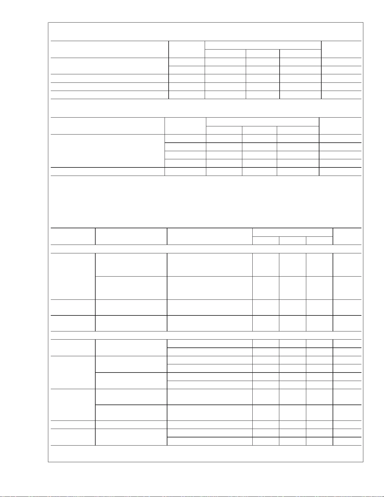
Absolute Maximum Ratings (Notes 1, 2)
LMX2364
Parameter Symbol
Power Supply Voltage V
Voltage on any pin with GND = 0V V
Storage Temperature Range T
Lead Temperature (Solder 4 sec.) T
Min Typ Max
Vcc
V
Vcp
CC
s
L
−0.3 6.5 V
−0.3 6.5 V
−0.3 VCC+ 0.3 V
−65 +150 ˚C
Value
+260 ˚C
Recommended Operating Conditions
Parameter Symbol
Power Supply Voltage V
Operating Temperature T
Note 1: “Absolute Maximum Ratings” indicate limits beyond which damage to the device may occur. Operating Ratings indicate conditions for which the device is
intended to be functional, but do not guarantee specific performance limits. For guaranteed specifications and test conditions, see the Electrical Characteristics. The
guaranteed specifications apply only for the test conditions listed.
Note 2: This Device is a high performance RF integrated circuit with an ESD rating
be done at ESD-free workstations.
Electrical Characteristics (V
VccRF
V
VccIF
V
VcpRF
V
VcpIF
Vcc=VVcp
A
= 3.0V; −40˚C ≤ TA≤ +85˚C except as specified)
Min Typ Max
2.7 5.5 V
V
VccRF
V
VccRF
V
CCIF
−40 +85 ˚C
<
2 kV and is ESD sensitive. Handling and assembly of this device should only
Value
V
VccRF
5.5 V
5.5 V
Units
Units
V
Symbol Parameter Conditions
I
PARAMETERS
CC
I
RF Power Supply Current, RF
CC
Synthesizer, Integer Mode
V
ENIF=VCLK=VDATA=VLE
= HIGH
V
ENRFV
FE=0
Power Supply Current, RF
Synthesizer, Fractional
Mode
ICCIF Power Supply Current, IF
Synthesizer
I
IF PD Power Down Current V
CC
V
ENIF=VCLK,=VDATA=VLE
=HIGH
V
ENRF
FE=1
V
ENRF=VCLK=VDATA=VLE
=HIGH
V
ENIF
ENRF=VENIF
V
CLK=VDATA=VLE
RF SYNTHESIZER PARAMETERS
f
FinRF
Operating Frequency Prescaler = 8/9/12/13 500 1200 MHz
Prescaler = 16/17/20/21 1200 2600 MHz
N Continuous N Divider
Range, Fractional Mode
Continuous N Divider
Range, Integer Mode
Prescaler = 8/9/12/13 40 4095
Prescaler = 16/17/20/21 80 8191
Prescaler = 8/9/12/13 40 266,239
Prescaler = 16/17/20/21 80 532,479
R R Divider Range,
Fractional Mode
R Divider Range, Integer
Mode (Note 3)
f
COMP
p
FinRF
Phase Detector Frequency 15 MHz
RF Input Sensitivity VCC= 3.0V −15 0 dBm
V
= 5.0V −10 0 dBm
CC
= LOW
= LOW
= LOW
=0 V
=LOW
Value
Min Typ Max
5.0 6.3 mA
7.2 8.0 mA
2.4 3.2 mA
5.0 20 µA
1 511
1 64,897
Units
www.national.com 4

LMX2364
Electrical Characteristics (V
Vcc=VVcp
Symbol Parameter Conditions
= 3.0V; −40˚C ≤ TA≤ +85˚C except as specified) (Continued)
Value
Min Typ Max
RF SYNTHESIZER PARAMETERS
I
SRCE RF Charge Pump Source
CPoutRF
Current
I
SINK RF Charge Pump Sink
CPoutRF
Current
I
TRI RF Charge Pump
CPoutRF
TRI-STATE Current
%MIS RF CP Sink vs. CP Source
I
CPoutRF
Mismatch
I
%V RF CP Current vs. CP
CPoutRF
Voltage
RF_CP=0
V
CPoutRF
RF_CP=1
V
CPoutRF
RF_CP=2
V
CPoutRF
RF_CP=3
V
CPoutRF
RF_CP=0
V
CPoutRF
RF_CP=1
V
CPoutRF
RF_CP=2
V
CPoutRF
RF_CP=3
V
CPoutRF
0.5 ≤ V
CPoutRF
V
CPoutRF
= 25˚C
T
A
0.5 ≤ V
CPoutRF
= 25˚C
T
A
=V
=V
=V
=V
=V
=V
=V
=V
=V
VcpRF
VcpRF
VcpRF
VcpRF
VcpRF
VcpRF
VcpRF
VcpRF
VcpRF
≤ V
≤ V
/2
/2
/2
/2
/2
/2
/2
/2
VcpRF
/2
VcpRF
−0.5
−0.5
1mA
4mA
8mA
16 mA
−1 mA
−4 mA
−8 mA
−16 mA
−10.0 10.0 nA
3.5 %
510%
RF_CP=0, 1, or 2
I
%TEMP RF CP Current vs.
CPoutRF
Temperature
VP
CPoutRF
=V
VcpRF
/2
810%
IF SYNTHESIZER PARAMETERS
f
FinIF
N IF Continuous N Divider
Operating Frequency 50 850 MHz
Range
56 262,143
R IF R Divider Range 3 32,767
f
COMP
p
FinIF
I
SRCE IF Charge Pump Source
CPoutIF
I
SINK IF Charge Pump Sink
CPoutIF
I
TRI IF Charge Pump
CPout
%MIS IF CP Sink vs. CP Source
I
CPoutIF
I
%V IF CP Current vs. CP
CPoutIF
I
%TEMP IF CP Current vs.
CPoutIF
Phase Detector Frequency 10 MHz
IF Input Sensitivity 2.7 ≤ V
IF_CP = 0
Current
V
CPoutIF
IF_CP = 1
V
CPoutIF
IF_CP = 0
Current
V
CPoutIF
IF_CP = 1
V
CPoutIF
0.5 ≤ V
TRI-STATE Current
V
CPoutIF
Mismatch
T
A
0.5 ≤ V
Voltage
T
A
V
CPoutIF
Temperature
≤ 5.5V −10 0 dBm
Vcc
100 µA
800 µA
−100 µA
−800 µA
5%
510%
8%
CPout
= 25˚C
CPoutIF
= 25˚C
=V
=V
=V
=V
=V
=V
VcpIF
VcpIF
VcpIF
VcpIF
≤ V
VcpIF
VcpIF
≤ V
/2
/2
/2
/2
VcpIF
/2
VcpIF
/2
−0.5
−0.5
−2.0 2.0 nA
Units
www.national.com5
Electrical Characteristics (V
Vcc=VVcp
= 3.0V; −40˚C ≤ TA≤ +85˚C except as specified) (Continued)
LMX2364
Symbol Parameter Conditions
Min Typ Max
Value
OSCILLATOR PARAMETERS
f
OSC
v
I
OSC
OSC
Oscillator Operating
Frequency
2 110 MHz
Oscillator Sensitivity OSCinRF, OSCinIF 0.5 V
Oscillator Input Current V
OSC=VVcc
V
= 0V −100 µA
OSC
Vcc
100 µA
DIGITAL INTERFACE (DATA, CLK, LE, ENIF, ENRF, Ftest/LD, FLoutRF, FLoutIF)
V
IH
V
IL
I
IH
I
IL
V
OH
V
OL
High-Level Input Voltage 2.7 ≤ V
3.2
≤ 3.2 1.6 V
Vcc
<
V
≤ 5.5 2 V
Vcc
Low-Level Input Voltage 0.4 V
High-Level Input Current VIH=V
CC
−1.0 1.0 µA
Low-Level Input Current VIL= 0 −1.0 1.0 µA
High-Level Output Voltage IOH= −500 µA VCC−0.4 V
Low-Level Output Voltage IOL= 500 µA 0.4 V
MICROWIRE INTERFACE TIMING
T
CS
T
CH
T
CWH
T
CWL
T
ES
T
EW
Data to Clock Set Up Time See Data Input Timing 50 ns
Data to Clock Hold Time See Data Input Timing 10 ns
Clock Pulse Width High See Data Input Timing 50 ns
Clock Pulse Width Low See Data Input Timing 50 ns
Clock to Load Enable Set
Up Time
See Data Input Timing
50 ns
Load Enable Pulse Width See Data Input Timing 50 ns
PHASE NOISE
L
(f) RF RF Synthesizer’s
F1Hz
Normalized Phase Noise
Contribution, Fractional
Mode (Note 4)
RF Synthesizer’s
Normalized Phase Noise
Contribution, Integer Mode
(Note 4)
(f) IF IF Synthesizer’s
L
F1Hz
Normalized Phase Noise
Contribution (Note 4)
Note 3: Some reference divider ratios between the minimum and maximum are not realizable. See the section on R divider programming for more details.
Note 4: Normalized Phase Noise Contribution is defined as: L
measured at an offset frequency, f, ina1HzBandwidth. The offset frequency, f, must be chosen sufficiently smaller than the PLL’s loop bandwidth, yet large enough
to avoid substantial phase noise contribution from the reference source.
RF_OM = 1 (Fractional Mode)
f=3KHz
TCXO Reference Source
RF_CP=1(4mA)
= LOW
V
ENIF
RF_OM = 0 (Integer Mode)
f=3KHz
TCXO Reference Source
RF_CP=2(4mA)
= LOW
V
ENIF
f=3KHz
TCXO Reference Source
IF_CP = 1 (800 mA)
= LOW
V
ENRF
(f) = L(f) – 20·log(N) – 10log(f
F1Hz
COMP
−208 dBc/Hz
−215 dBc/Hz
−212 dBc/Hz
) where L(f) is defined as the single side band phase noise
Units
V
www.national.com 6
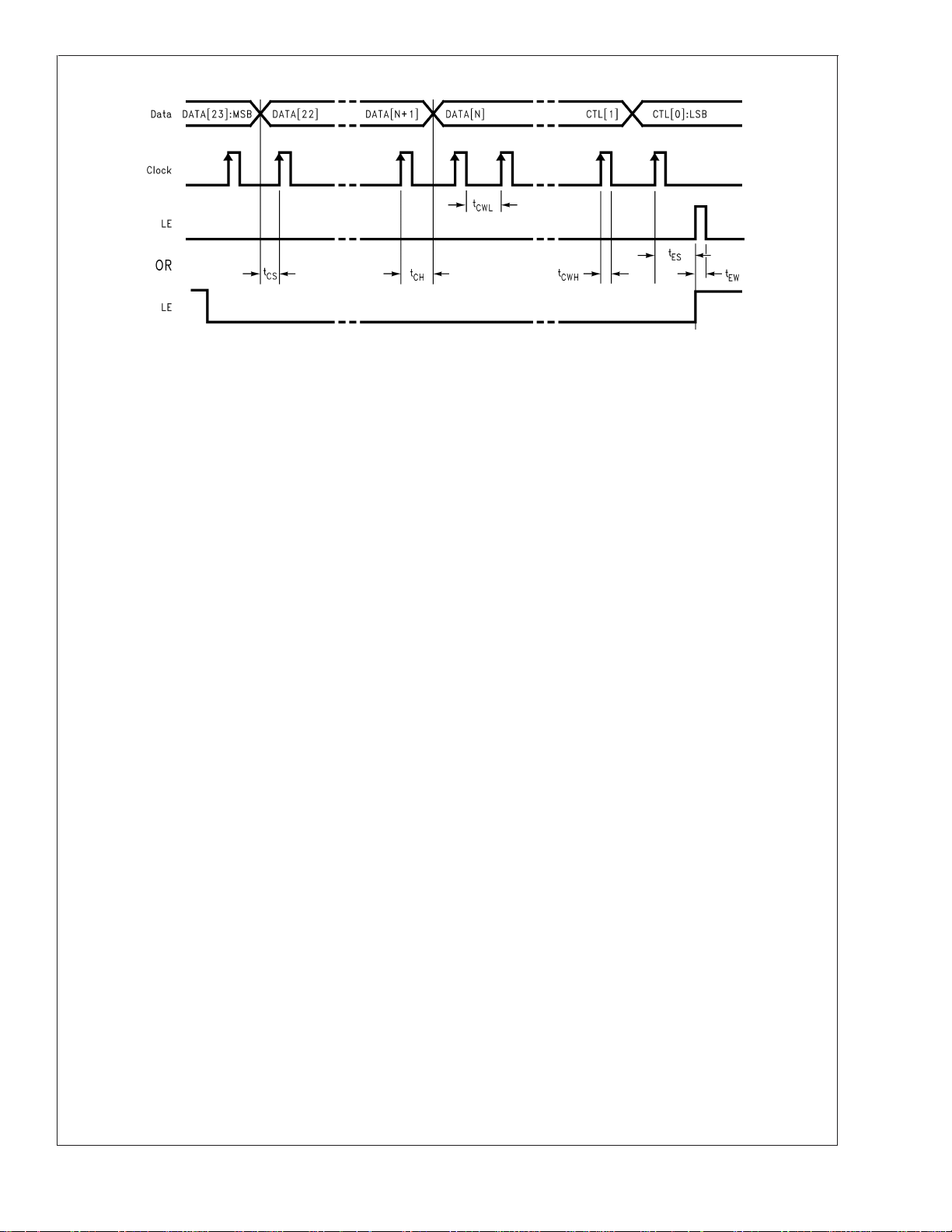
Serial Data Input Timing
20050603
Note: Data is shifted MSB first into the MICROWIRE shift register on the rising edge of the Clock signal. When a rising edge is seen on the LE pulse, these values
are actually loaded into the PLL target registers.
Since the data is clocked in on the rising edge of the LE pulse, the programming time of one register can be eliminated by sending the Data and Clock signals
in advance and delaying the LE pulse until it is desired that the values are to be loaded.
Note: The Serial Data Input Timing is tested using a symmetrical waveform around V
@
VCC=2.7V and 2.6V@VCC= 3.3V.
/2. The test waveform has an edge rate of 0.6 V/ns with amplitudes of 2.2V
CC
LMX2364
www.national.com7

Typical Performance Characteristics
LMX2364
RF PLL 1 Hz Normalized Phase Noise (Fractional Mode)
20050672
IF PLL 1 Hz Normalized Phase Noise
www.national.com 8
20050673
Typical Performance Characteristics (Continued)
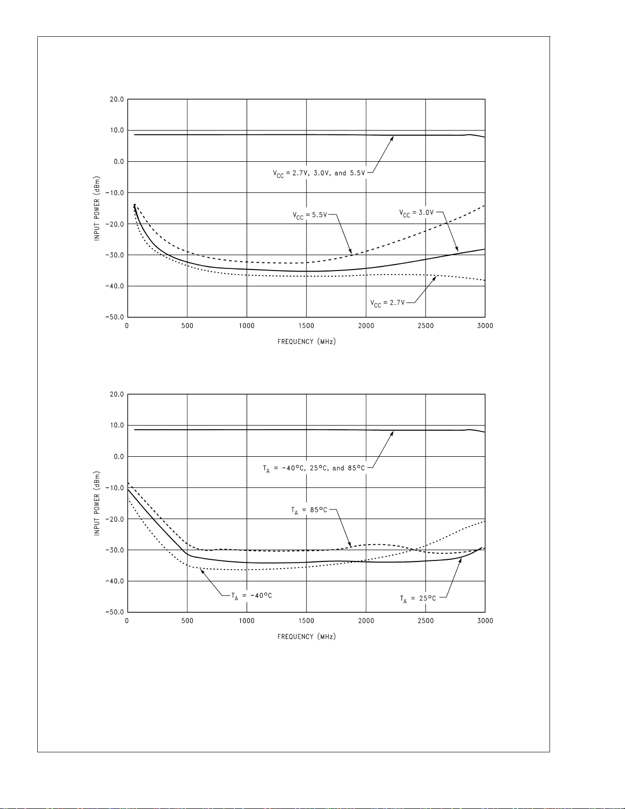
RF N Counter Sensitivity
T
= 25˚C
A
LMX2364
RF N Counter Sensitivity
Vcc = 3.0V
20050645
20050646
www.national.com9

Typical Performance Characteristics (Continued)
LMX2364
IF N Counter Sensitivity
T
= 25˚C
A
IF N Counter Sensitivity
Vcc = 3.0V
20050647
www.national.com 10
20050648

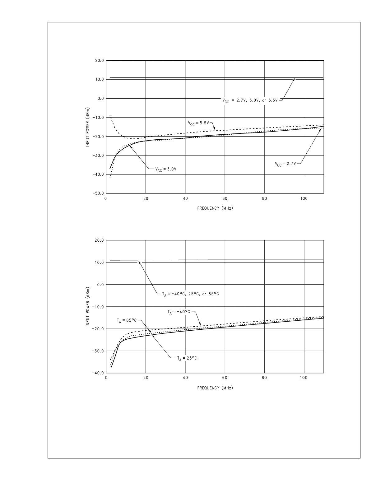
Typical Performance Characteristics (Continued)
OSCinRF Counter Sensitivity
T
= 25˚C
A
LMX2364
OSCinRF Counter Sensitivity
Vcc = 3.0V
20050649
20050650
www.national.com11
Typical Performance Characteristics (Continued)
LMX2364
OSCinIF Counter Sensitivity
T
= 25˚C
A
OSCinIF Counter Sensitivity
Vcc = 3.0V
20050651
www.national.com 12
20050652
 Loading...