

查询LMV243供应商
LMV243
Single-Channel, Quad-Band GSM Power Controller in
micro SMD
LMV243 Single-Channel, Quad-Band GSM Power Controller in micro SMD
May 2002
General Description
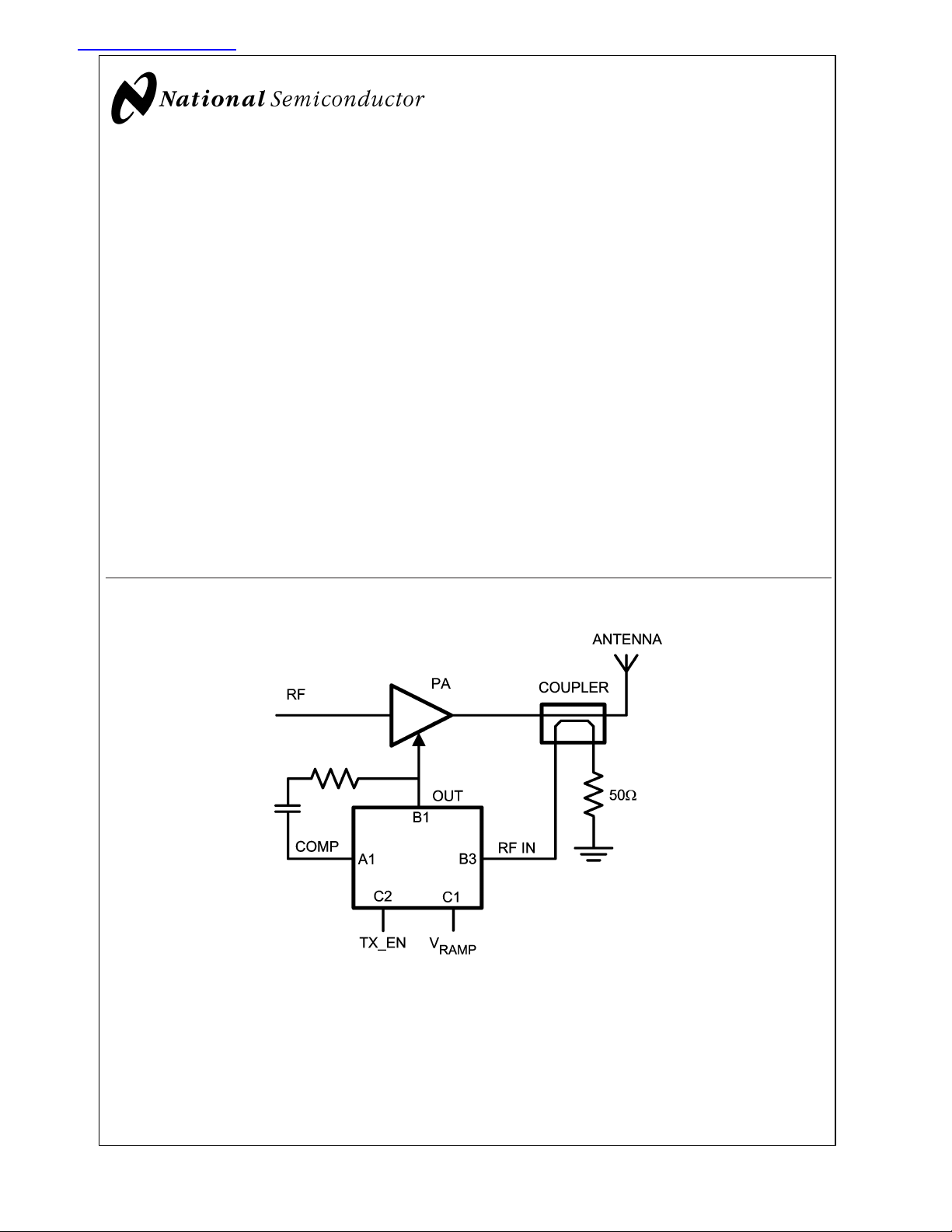
The device is intended for use within an RF transmit power
control loopin GSM mobile phones and supports GaAs HBT
and bipolar RF single supply power amplifiers. The circuit
operates with a single supply from 2.7V to 3.3V.
The LMV243 contains an RF detector, error amplifier, ramp
V/I converter and output driver. The LMV243 input interface
consists of the RF input, Ramp voltage, and a digital input to
perform the function ’Shutdown/Transmit Enable’. The device will be active in the case TX_EN = HI, otherwise, the
device goes into a low power consumption shutdown mode.
During shutdown the output will be in high impedance
(tri-state).
A single external RC combination is used to provide stable
operations that accommodates individual PA characteristics.
The LMV243 is offered in a 8-bump micro SMD 1.5mm x
1.5mm package. This space savings package supports flexible product placement almost anywhere in the circuitboard.
Typical Application
Features
(Typical Unless Otherwise Noted)
n 50dB RF detection range (typical)
n micro SMD package 1.5mm x 1.5mm x 0.995mm
n Support of GaAs HBT, bipolar technology
n Quad-band operation
n Shutdown mode for Power Save in Rx slot
n GPRS compliant
n External loop compensation option
n Accurate temperature compensation
n Frequency range is 450MHz to 2GHz
Applications
n GSM mobile phone
n AGC for digital audio
n TDMA RF control
n Wireless LAN
20029034
© 2002 National Semiconductor Corporation DS200290 www.national.com
Absolute Maximum Ratings (Note 1)
If Military/Aerospace specified devices are required,
LMV243
please contact theNational Semiconductor SalesOffice/
Distributors for availability and specifications.
Supply Voltage
V
- GND 4V Max
DD
ESD Tolerance (Note 2)
Human Body Model 2000V
Machine Model 200V
Storage Temperature Range −65˚C to 150˚C
Junction Temperature (Note 6) 150˚C Max
Mounting Temperature
Infrared or convection (20 sec) 235˚C
Operating Ratings (Note 1)
Nominal Supply Voltage 2.7V to 3.3V
<
Temperature Range −40˚C
V
Voltage Range 0V to 2V
RAMP
V
Voltage Range 0V to 2V
HOME
RF Frequency Range 450MHz to 2GHz
<
T
85˚C
J
Electrical Characteristics Unless otherwise specified, all limits are guaranteed to T
= 25˚C. VDD= 2.8V.
J
Boldface limits apply at temperature extremes.
Symbol Parameter Condition Min Typ Max Units
I
DD
Supply Current V
=(VDD- GND)/2 8.7 10.5
OUT
mA
12.5
In Shutdown (TX_EN = 0.8V)
=(VDD- GND)/2
V
OUT
V
HIGH
V
LOW
T
ON
Logic Level to Enable Power (Note 7) 1.8 V
Logic Level to Disable Power (Note 7) 0.8 V
Turn-on- Time from Shutdown 3.7 6.5
4.6 30 µA
µs
7.5
I
EN
Current into TX_EN Pin 0.108 5 µA
RAMP Amplifier
V
RD
1/R
RAMP
I
OUT RAMP
V
Deadband 170
RAMP
150
210 250
270
mV
Transconductance (Note 8) 78 µa/V
Ramp Amplifier Output Current V
=2V 100 140 µA
RAMP
RF Input
P
IN
RF Input Power Range (Note 5) 20kΩ // 27pF between V
and V
COMP
OUT
−50
+5
−63
dBm
dBV
−7
Logarithmic Slope (Note 9)
Logarithmic Intercept (Note 9)
R
IN
C
IN
DC Resistance (Note 8) 50 Ω
Input Capacitance (Note 8) 0.5 pF
@
900MHz, 20kΩ // 27pF
between V
@
1800MHz, 20kΩ // 27pF
between V
@
1900MHz, 20kΩ // 27pF
between V
@
900MHz, 20kΩ // 27pF
between V
@
1800MHz, 20kΩ // 27pF
between V
@
1900MHz, 20kΩ // 27pF
between V
OUT
OUT
OUT
OUT
OUT
OUT
and V
and V
and V
and V
and V
and V
COMP
COMP
COMP
COMP
COMP
COMP
−1.79
−1.89
−1.89
−50.5
−46.9
−45.9
µa/dB
dBm
Error Amplifier
GBW Gain-Bandwidth Product (Note 8) 7.6 MHz
www.national.com 2
LMV243
Electrical Characteristics Unless otherwise specified, all limits are guaranteed to T
= 25˚C. VDD= 2.8V.
J
Boldface limits apply at temperature extremes. (Continued)
Symbol Parameter Condition Min Typ Max Units
V
O
Output Swing from Rail Sourcing, IO= 5mA 55 85
105
Sinking, I
= −5mA 45 75
O
mV
95
I
O
e
n
Output Short Circuit Current
(Note 3)
Sourcing, VO=0V 25 145
Sinking, V
= 2.8V 25 180
O
Output Referred Noise RF input = 1800 MHz,
mA
700 nV/
-10dBm, 20kΩ // 27pF
between V
=1.4V, set by V
V
OUT
OUT
and V
COMP
RAMP
,
,
(Note 8)
SR Slew Rate 8
11 V/µs
5
Note 1: Absolute Maximum Ratings indicate limits beyond which damage to the device may occur. Operating Ratings indicate conditions for which the device is
intended to be functional, but specific performance is not guaranteed. For guaranteed specifications and the test conditions, see the Electrical Characteristics.
Note 2: Human body model: 1.5kΩ in series with 100pF. Machine model, 0Ω in series with 100pF.
Note 3: Shorting circuit output to either V
Note 4: Electrical Table values apply only for factory testing conditions at the temperature indicated. Factory testing conditions result in very limited self-heating of
the device such that T
Note 5: Power in dBV = dBm + 13 when the impedance is 50Ω.
Note 6: The maximum power dissipation is a function of T
(T
J(MAX)-TA
Note 7: All limits are guaranteed by design or statistical analysis
Note 8: Typical values represent the most likely parametric norm.
Note 9: Slope and intercept are calculated from graphs ’V
)/θJA. All numbers apply for packages soldered directly into a PC board
. No guarantee of parametric performance is indicated in the electrical tables under conditions of internal self-heating where T
J=TA
+
or V−will adversely affect reliability.
, θJAand TA. The maximum allowable power dissipation at any ambient temperature is PD=
J(MAX)
vs. RF input Power’ where the current is obtained by division of the voltage by 20kΩ.
OUT
J
>
TA.
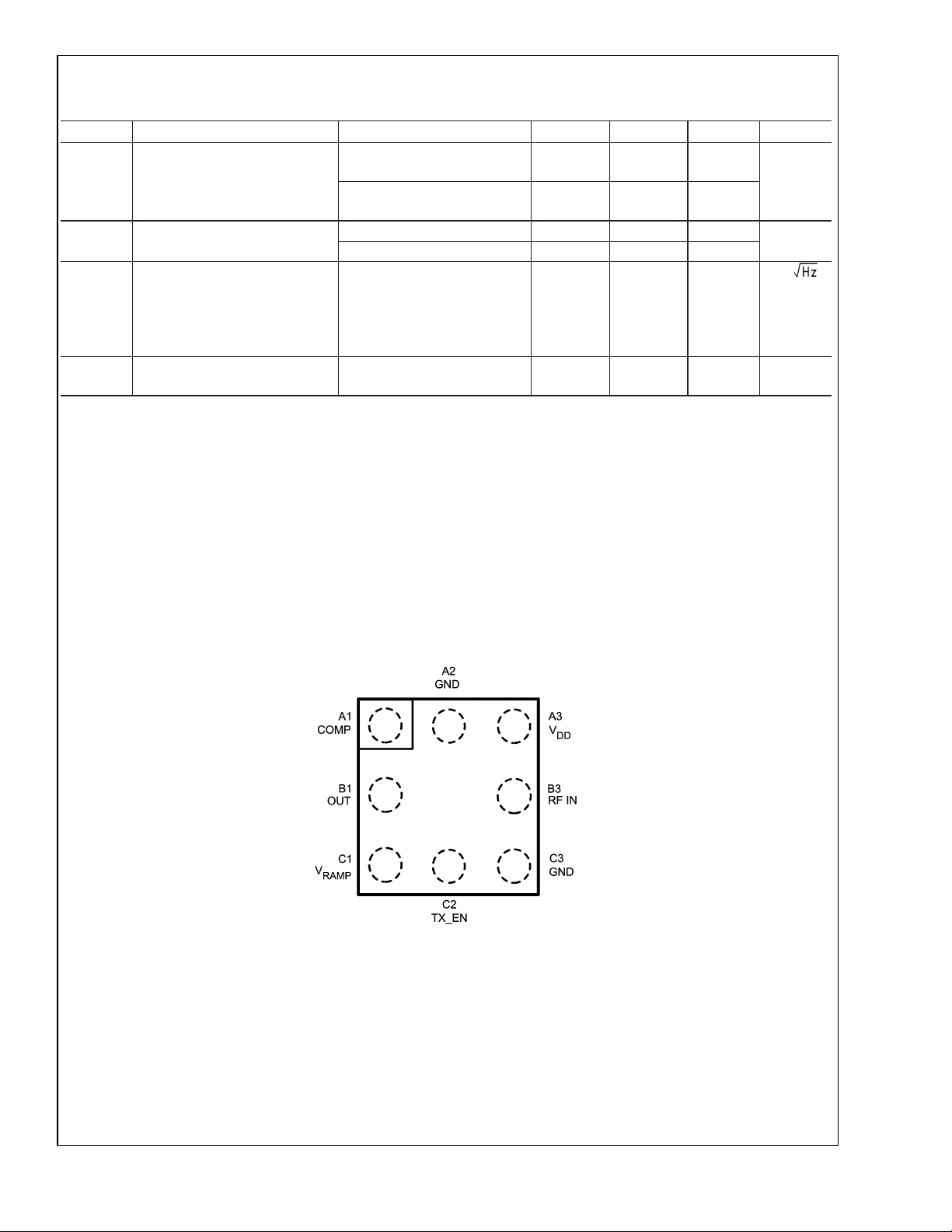
Connection Diagram
8-Bump micro SMD
20029035
Top View
www.national.com3
Pin Descriptions
LMV243
Power Supply A3 V
Digital Inputs C2 TX_EN A Logic High to enable device.
Analog Inputs B3 RF IN RF Input connected to the Coupler output with optional attenuation to measure the
Compensation A1 Comp Connects an external RC network between the Comp pin and the Output pin for an
Output B1 Out A rail-to-rail output capable of sourcing 25mA and sinking 25mA, with less than 200mV
Note: 1. All inputs and outputs are referenced to GND (pin A2, C3).
2. For the digital inputs, a LOW is
3. RF power detection is performed internally in the LMV243 and only an RF power coupler with optional extra attenuation has to be used.
Pin Name Description
DD
Supply Voltage
A2, C3 GND Power Ground. Operation requires both pins be grounded.
Power Amplifier (PA) / Antenna RF power levels.
C1 RAMP IN Sets the RF output power level. The useful input voltage range is from 0.2V to 1.8V,
although voltages from 0V to V
are allowed.
DD
overall loop compensation and to control the closed loop frequency response.
Conventional loop stability techniques can be used in selecting this network, such as
Bode plots. A good starting value for the RC combination will be C = 68pF andR=0Ω.
total voltage drop over the specified temperature. The output is free from glitches when
enabled by TX_EN. When TX_EN is low, the output voltage is near GND.
<
0.8V and a HIGH is>1.8V.
Ordering Information
Package Part Number Package Marking Transport Media NSC Drawing
8-Bump micro SMD
LMV243BL 01 1k Units Tape and Reel
LMV243BLX 01 3k Units tape and Reel
BLA08AAC
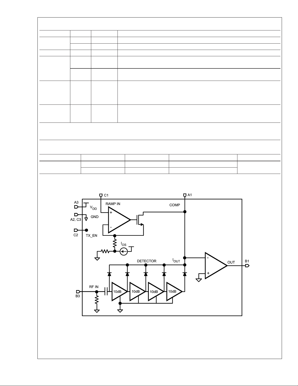
Block Diagram
20029036
FIGURE 1.
www.national.com 4
 Loading...