


查询LMV232供应商
LMV232
Dual-Channel Integrated Mean Square Power Detector
for CDMA & WCDMA
LMV232 Dual-Channel Integrated Mean Square Power Detector for CDMA & WCDMA
February 2005
General Description
The LMV232 dual RF detector is designed for RF transmit
power measurement in mobile phones. This dual mean
square IC is especially suited for accurate power measurement of RF signals exhibiting high peak-to-average ratios
used in 3G and UMTS/CDMA applications. The LMV232
saves calibration steps and system certification and is highly
accurate. The circuit operates with a single supply from 2.5
to 3.3V.
The LMV232 contains a mean square detector with two
sequentially selectable RF inputs. The RF input power range
of the device has been optimized for use with a 20 dB
directional coupler, without the need for additional external
components. A single external RC combination between FB
and OUT provides an externally configurable gain and LF
filter bandwidth of the device.
The device has two digital interfaces. A shutdown function is
available to set the device in a low-power shutdown mode. In
case SD = HIGH, the device is in shutdown, if SD = LOW the
device is active. The Band-Select function controls the selection of the active RF input channel. In case BS = HIGH,
1 is active. In case BS = LOW, RFIN2 is active.
RF
IN
The dual mean square detector is offered in an 8-bump
micro SMD 1.5 x 1.5 x 0.6 mm package. This micro SMD
package has the smallest footprint and height.
Typical Application
Features
n>20 dB square-law detection range
n 2 sequentially selectable RF inputs
n Low power consumption shutdown mode
n Externally configurable gain and LF filter bandwidth.
n Internal 50Ω RF termination impedance
n Optimized for use with 20 dB directional coupler
n Lead free 8-bump micro SMD package 1.5 x 1.5 x 0.6
mm
Applications
n 3G mobile communications
n UMTS
n WCDMA
n CDMA2000
n TD-SCDMA
n RF control
n Wireless LAN
n PC Card and GPS modules
20127801
© 2005 National Semiconductor Corporation DS201278 www.national.com
Absolute Maximum Ratings (Note 1)
If Military/Aerospace specified devices are required,
LMV232
please contact the National Semiconductor Sales Office/
Distributors for availability and specifications.
Supply Voltage
- GND 3.6V Max
V
DD
ESD Tolerance (Note 2)
Human Body Model 2000V
Machine Model 200V
Junction Temperature (Note 3) 150˚C Max
Mounting Temperature
Infrared or Convection (20 sec) 235˚C
Operating Ratings (Note 1)
Supply Voltage 2.5V to 3.3V
Operating Temperature Range -40˚C to +85˚C
RF Frequency Range 50 MHz to 2 GHz
Storage Temperature Range -65˚C to 150˚C
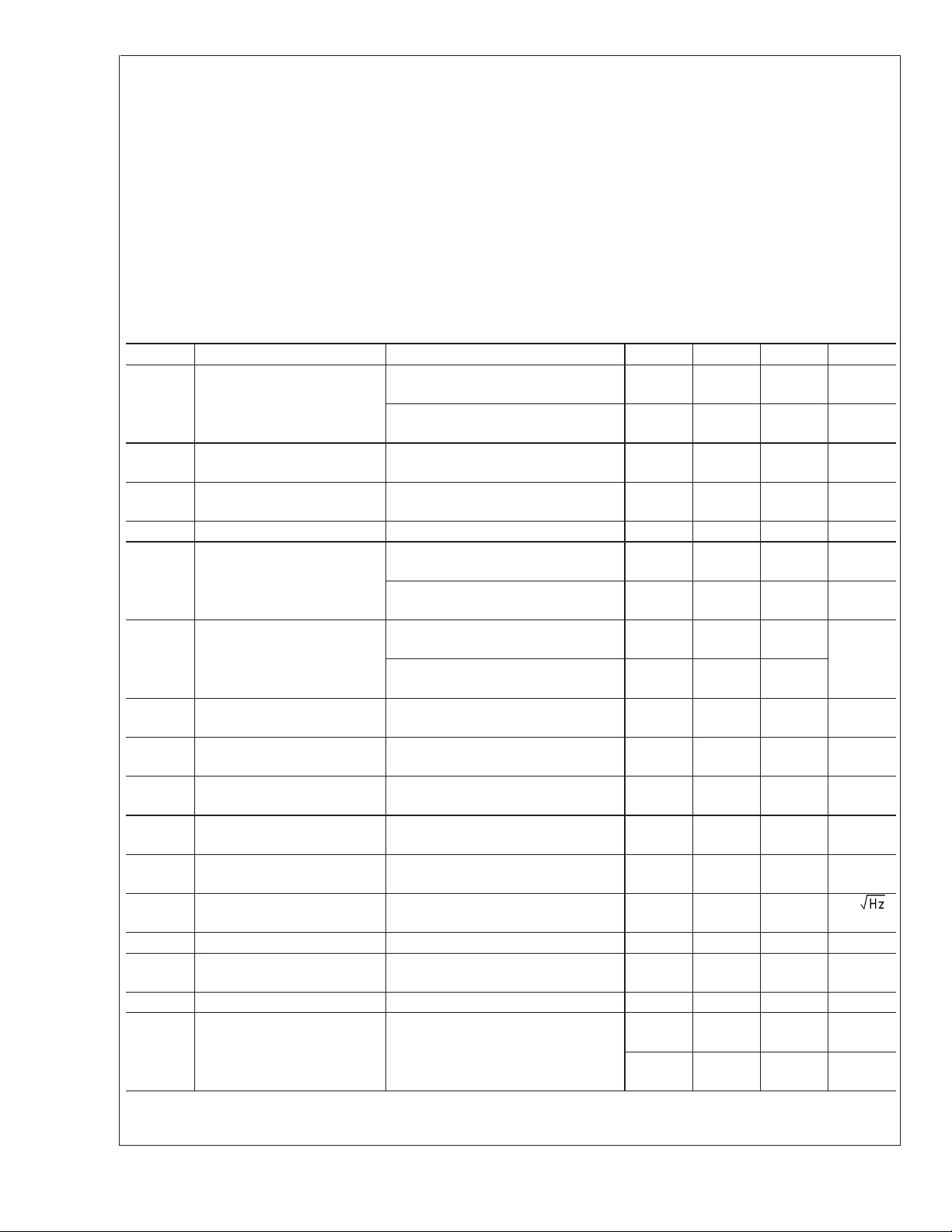
2.7 DC and AC Electrical Characteristics
Unless otherwise specified, all limits are guaranteed to VDD= 2.7V; TJ= 25˚C. Boldface limits apply at temperature extremes.
(Note 4)
Symbol Parameter Condition Min Typ Max Units
I
DD
Supply Current Active Mode: SD = LOW, No RF Input
Power Present
Shutdown: SD = 1.8V, No RF Input
Power Present
V
LOW
BS and SD Logic Low Level
(Note 6)
V
HIGH
BS and SD Logic High Level
1.8 V
(Note 6)
I
BS,ISD
V
OUT
Current into BS and SD pins 5 µA
Output Voltage Swing From Positive Rail, Sourcing,
FB = 0V, I
OUT
=1mA
From Negative Rail, Sinking,
I
OUT
FB = 2.7V, I
Output Short Circuit Sourcing, FB = 0V, V
OUT
=−1mA
OUT
= 2.6V 3.7
2.7
Sinking, FB = 2.7V, V
= 0.1V 3.7
OUT
2.7
V
OUT
Output Voltage (Pedestal) No RF Input Power 235
230
V
PED
Pedestal Variation Over
Temperature (Note 10)
I
OS
Offset Current Variation Over
Temperature (Note 10)
t
ON
Turn-on-Time (Note 9) No RF Input Power Present, Output
Loaded with 10 pF
t
R
Rise Time (Note 7) Step from No Power to 0 dBm
Applied, Output Loaded with 10 pF
e
n
Output Referred Voltage Noise RF Input = 1800 MHz, -10 dBm,
Measured at 10 kHz
GBW Gain Bandwidth Product 3.7 MHz
SR Slew Rate 1.8
1.0
R
IN
P
IN
DC Resistance (Note 7) 50.8 Ω
RF Input Power Range RF Input Frequency = 900 MHz -11
9.8 11
13
0.09 5
30
0.8 V
20 80
90
20 60
70
5.1
5.5
254 275
280
5.4
1.17
2.0 6.0
4.5
400 nV/
3.0 V/µs
+13
-24
0
mA
µA
mV
mV
mA
mV
mV
µA
µs
µs
dBm
dBV
www.national.com 2

2.7 DC and AC Electrical Characteristics (Continued)
Unless otherwise specified, all limits are guaranteed to VDD= 2.7V; TJ= 25˚C. Boldface limits apply at temperature extremes.
(Note 4)
Symbol Parameter Condition Min Typ Max Units
K
DET
f
LOW
f
HIGH
A
ISO
Note 1: Absolute Maximum Ratings indicate limits beyond which damage to the device may occur. Operating Ratings indicate conditions for which the device is
intended to be functional, but specific performance is not guaranteed. For guaranteed specifications and the test conditions, see the Electrical Characteristics.
Note 2: Human body model: 1.5 kΩ in series with 100 pF. Machine model, 0Ω in series with 100 pF.
Note 3: The maximum power dissipation is a function of T
(T
J(MAX)-TA
Note 4: Electrical Table values apply only for factory testing conditions at the temperature indicated. Factory testing conditions result in very limited self-heating of
the device such that T
Note 5: Power in dBV = dBm + 13 when the impedance is 50Ω.
Note 6: All limits are guaranteed by design or statistical analysis.
Note 7: Typical values represent the most likely parametric norm.
Note 8: Device is set in active mode with a 10 kΩ resistor from V
pin using a 100 pF coupling capacitor.
Note 9: Turn-on time is measured by connecting a 10 kΩ resistor to the RF
of resistor R2 and capacitor C adds an additional delay.
Note 10: Typical numbers represent the 3-sigma value of 10k units. 3-sigma value of variation between −40˚C / 25˚C and variation between 25˚C / 85˚C.
Detection Slope 900 MHz 21
1800 MHz 10
1900 MHz 10
µA/mW
2000 MHz 10
LF Input Corner Frequency Lower −3 dB Point of Detection Slope 60 MHz
HF Input Corner Frequency Upper −3 dB Point of Detection Slope 1.0 GHz
Channel Isolation 900 MHz 58
1800 MHz 62
1900 MHz 58
dB
2000 MHz 55
, θJAand TA. The maximum allowable power dissipation at any ambient temperature is PD=
)/θJA. All numbers apply for packages soldered directly into a PC board.
. No guarantee of parametric performance is indicated in the electrical tables under conditions of internal self-heating where T
J=TA
J(MAX)
to RFIN/EN. RF signal is applied using a 50Ω RF signal generator AC coupled to the RFIN/E
DD
pin. Be aware that in the actual application on the front page, the RC-time constant
IN/EN
>
J
LMV232
TA.
N
www.national.com3
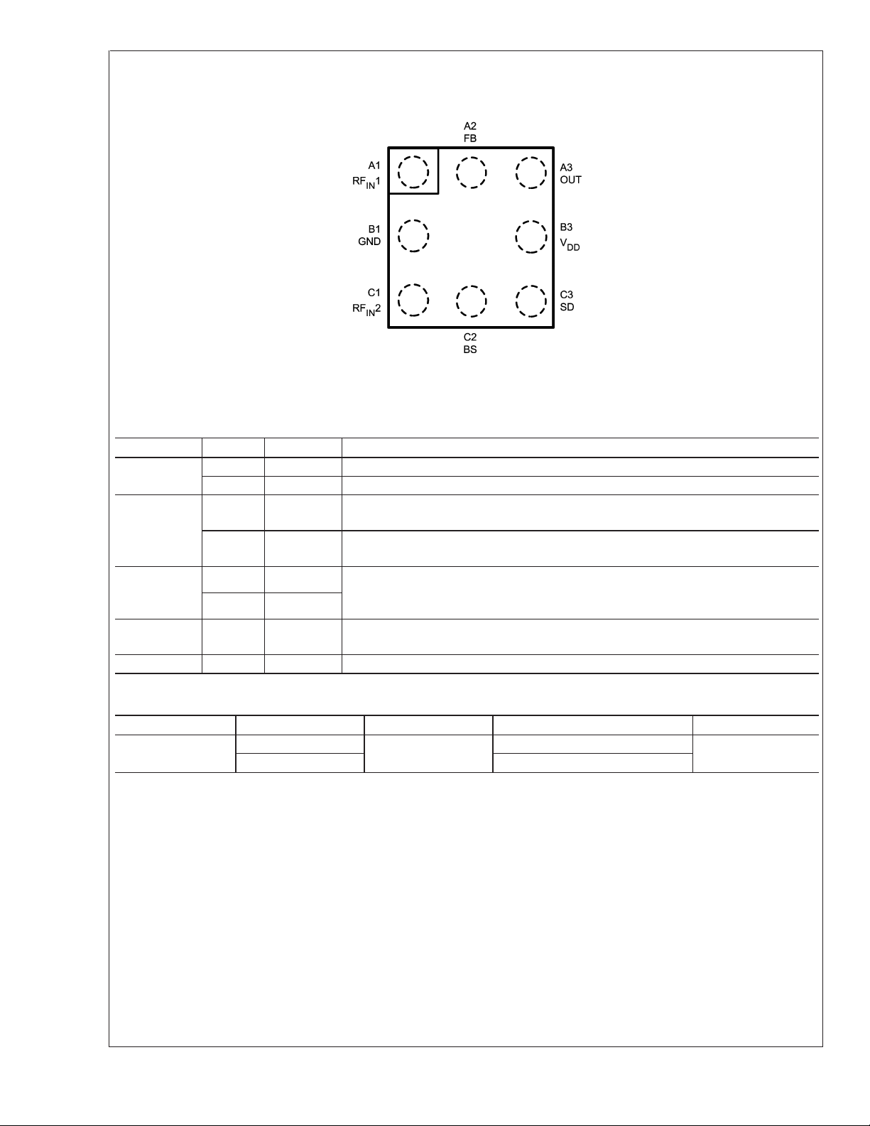
Connection Diagram
LMV232
8-Bump micro SMD
20127802
Top View
Pin Description
Pin Name Description
Power Supply B3 V
DD
B1 GND Power Ground
Digital Inputs C3 SD Schmitt-triggered Shutdown. The device is active for SD = LOW. For SD = HIGH, it is
C2 BS Schmitt-triggered Band Select pin. When BS = HIGH, RF
Analog Inputs A1 RF
C1 RF
Feedback A2 FB Connected to inverting input of output amplifier. Enables user-configurable gain and
Output A3 Out Amplifier output
Positive Supply Voltage
brought into a low-power shutdown mode.
1 is selected, when BS =
IN
LOW, RF
1 RF Input connected to the coupler output with optional attenuation to measure the
IN
Power Amplifier (PA) / Antenna RF power levels. Both RF inputs of the device are
2
IN
internally terminated with a 50Ω resistance.
2 is selected.
IN
bandwidth through external feedback network.
Ordering Information
Package Part Number Package Marking Transport Media NSC Drawing
8-Bump micro SMD
Note: This product is only offered with lead free bumps.
www.national.com 4
LMV232TL
LMV232TLX 3k Units Tape and Reel
A
I02
250 Units Tape and Reel
TLA08AAA
 Loading...