

November 2003
LMS485E
Low Power RS-485 / RS-422 Differential Bus Transceiver
LMS485E Low Power RS-485 / RS-422 Differential Bus Transceiver
General Description
The LMS485E is a low power differential bus/line transceiver
designed for high speed bidirectional data communication on
multipoint bus transmission lines. It is designed for balanced
transmission lines. It meets ANSI Standards TIA/EIA
RS422-B, TIA/EIA RS485-A and ITU recommendation and
V.11 and X.27. The driver outputs and receiver inputs have
±
15kV ESD protection. The LMS485E combines a TRI-
™
STATE
both of which operate from a single 5.0V power supply. The
driver and receiver have an active high and active low,
respectively, that can be externally connected to function as
a direction control. The driver outputs and receiver inputs are
internally connected to form a differential input/output (I/O)
bus port that is designed to offer minimum loading to bus
whenever the driver is disabled or when V
ports feature wide positive and negative common mode
voltage ranges, making the device suitable for multipoint
applications in noisy environments. The LMS485E is available in 8-Pin SOIC and 8-pin DIP packages. It is a drop-in
replacement to Maxim’s MAX485E.
differential line driver and differential input receiver,
= 0V. These
CC
Typical Application
Features
n Meet ANSI standard RS-485 and RS-422
n Data rate 2.5 Mbps
n Single supply voltage operation, 5V
n Wide input and output voltage range
n Thermal shutdown protection
n Short circuit protection
n Low quiescent current 800µA (max)
n Allows up to 32 transceivers on the bus
n Open circuit fail-safe for receiver
n Extended operating temperature range −40˚C to 85˚C
n Drop-in replacement to MAX485E
n Available in 8-pin SOIC and 8-pin DIP packages
Applications
n Low power RS-485 systems
n Network hubs, bridges, and routers
n Point of sales equipment (ATM, barcode scanners,…)
n Local area networks (LAN)
n Integrated service digital network (ISDN)
n Industrial programmable logic controllers
n High speed parallel and serial applications
n Multipoint applications with noisy environment
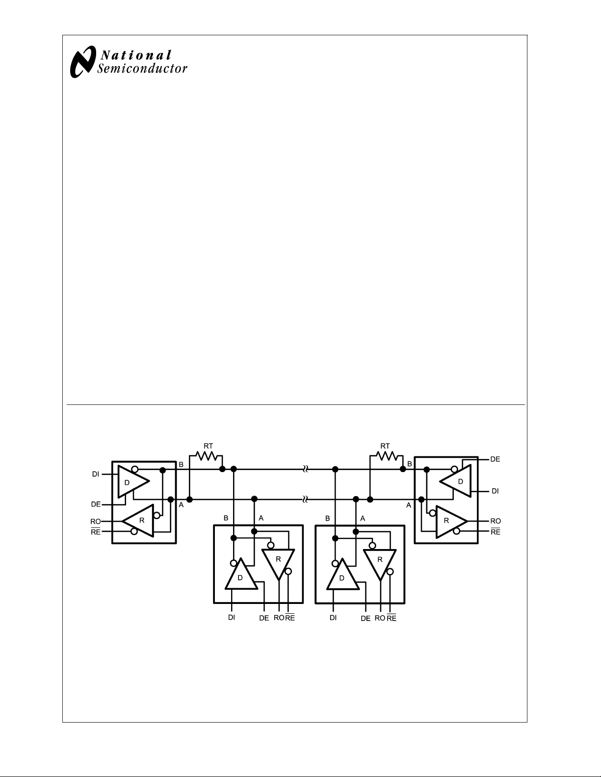
A typical multipoint application is shown in the above figure. Terminating resistor, RT are typically required but only located at the two ends of the cable.
Pull-up and pull-down resistors maybe required at the end of the bus to provide fail-safe biasing. The biasing resistors provide a bias to the cable when all
drivers are in TRI-STATE, See National Application Note, AN-847 for further information.
© 2003 National Semiconductor Corporation DS200866 www.national.com
20086601
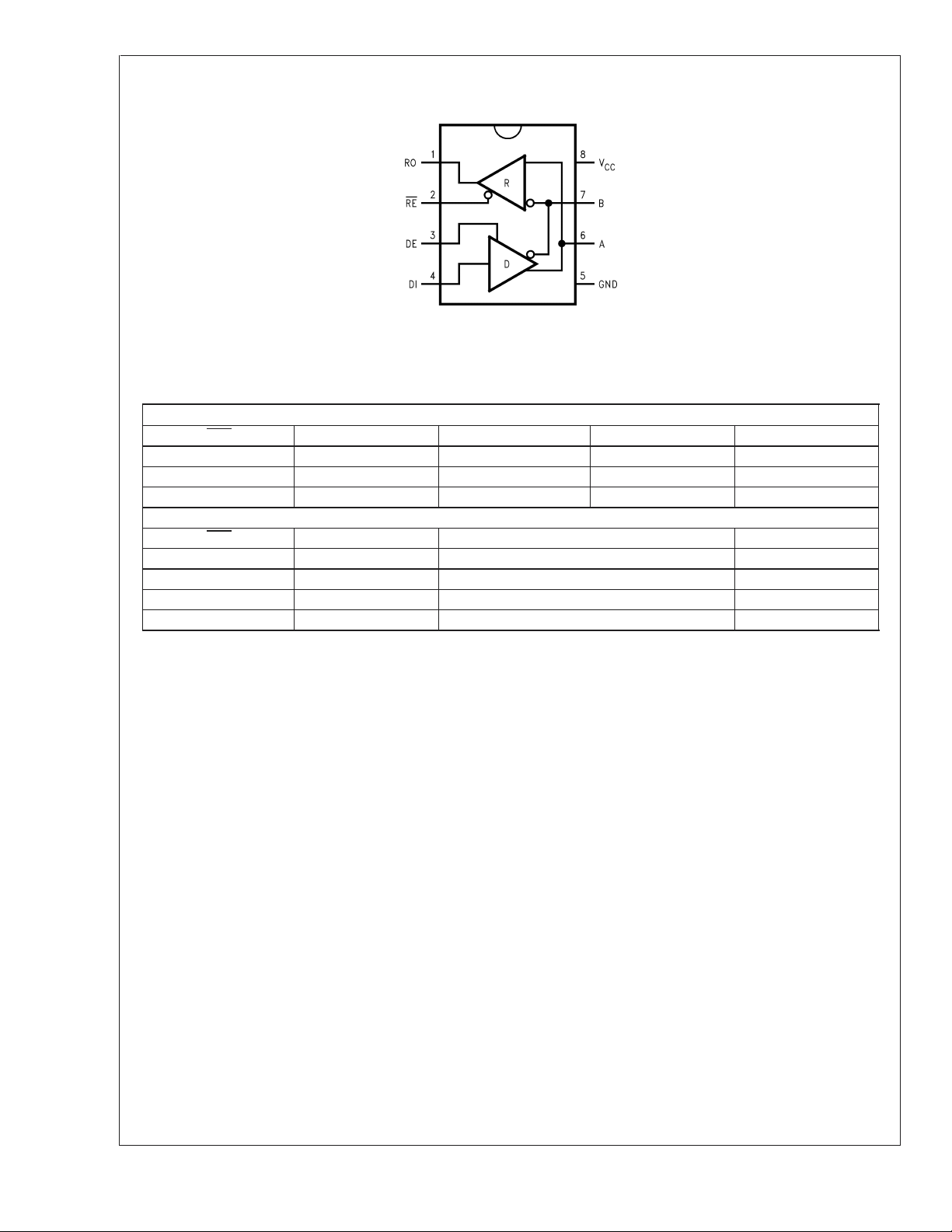
Connection Diagram
LMS485E
Truth Table
DRIVER SECTION
RECEIVER SECTION
8-Pin SOIC / DIP
Top View
20086602
*
RE
DE DI A B
XHHHL
XHL LH
XLXZZ
*
RE
DE A-B RO
LL ≥ +0.2V H
LL ≤ −0.2V L
HX X Z
L L OPEN
*
H
Note:*= Non Terminated, Open Input only
X = Irrelevant
Z = TRI-STATE
H = High level
L = Low level
www.national.com 2
Pin Descriptions
Pin#I/O Name Function
1 O RO Receiver Output: If A
will be high also if the inputs (A and B) are open (non-terminated).
2I RE
3 I DE Driver Output Enable: The driver outputs (A and B) are enabled when DE is high; they are in
4 I DI Driver Input: A low on DI forces A low and B high while a high on DI forces A high and B low
5 NA GND Ground
6 I/O A Non-inverting Driver Output and Receiver Input pin. Driver output levels conform to RS-485
7 I/O B Inverting Driver Output and Receiver Input pin. Driver Output levels conform to RS-485 signaling
8NAV
*
CC
Receiver Output Enable: RO is enabled when RE*is low; RO is in TRI-STATEwhen RE*is high
TRI-STATETRI-STATE
(see below)
when the driver is enabled
signaling levels
levels
Power Supply: 4.75V ≤ VCC≤ 5.25V
>
B by 200 mV, RO will be high; If A<B by 200 mV, RO will be low. RO
®
when DE is low. Pins A and B also function as the receiver input pins
Ordering Information
Package Part Number Package Marking Transport Media NSC Drawing
8-Pin SOIC
8-Pin DIP
LMS485ECM
LMS485ECMX 2.5k Units Tape and Reel
LMS485EIM
LMS485EIMX 2.5k Units Tape and Reel
LMS485ECNA LMS485ECNA 40 Units/Rail
LMS485EINA LMS485EINA 40 Units/Rail
LMS485ECM
LMS485EIM
95 Units/Rail
95 Units/Rail
M08A
N08E
LMS485E
www.national.com3
Absolute Maximum Ratings (Note 1)
If Military/Aerospace specified devices are required,
please contact the National Semiconductor Sales Office/
LMS485E
Distributors for availability and specifications.
Supply Voltage, V
Input Voltage, V
(Note 2) 6V
CC
(DI, DE, or RE) −0.3V to VCC+ 0.3V
IN
Voltage Range at Bus Terminals (AB) −7V to 12V
Receiver Output −0.3V to V
Package Thermal Impedance, θ
JA
SOIC 125˚ C/W
DIP 92˚ C/W
Junction Temperature (Note 3) 150˚C
Operating Free-Air Temperature
Range, T
A
Commercial 0˚C to 70˚C
Industrial −40˚C to 85˚C
Storage Temperature Range −65˚C to 150˚C
Soldering Information
Infrared or Convection (20 sec.) 235˚C
Lead Temperature Range +260˚C
CC
+ 0.3V
ESD Rating (Human Body Model)(Note 4)
Bus Pins 15kV
Other Pins 2kV
ESD Rating (Machine Model)
All Pins 200V
Operating Ratings
Min Nom Max
Supply Voltage, V
CC
Voltage at any Bus Terminal
(Separately or Common Mode)
High-Level Input Voltage, V
(Note 5)
Low-Level Input Voltage, V
(Note 5)
Differential Input Voltage, V
(Note 6)
4.75 5.0 5.25 V
−7 12 V
IH
IL
ID
2V
Electrical Characteristics
Over recommended ranges of supply voltage and operating free-air temperature (unless otherwise noted)
Symbol Parameter Conditions Min Typ Max Units
Driver Section
|V
| Differential Output Voltage R =∞(Figure 1) 5.25 V
OD1
|V
| Differential Output Voltage R = 50Ω (Figure 1) , RS-422 2.0 V
OD2
R=27Ω (Figure 1) , RS-485 1.5 5.0
∆V
OD
V
OC
∆V
OC
V
IH
V
IL
I
IN1
Receiver Section
I
IN2
V
TH
∆V
TH
V
OH
Change in Magnitude of
R=27Ω or 50Ω (Figure 1) , (Note 7) 0.2 V
Driver Differential Output
Voltage for Complementary
Output States
Common Mode Output
R=27Ω or 50Ω (Figure 1) 3.0
Voltage
Change in Magnitude of
R=27Ω or 50Ω (Figure 1), (Note 7) 0.2 V
Driver Common-Mode Output
Voltage for Complementary
Output States
CMOS Input Logic Threshold
DE, DI, RE 2.0 V
High
CMOS Input Logic Threshold
DE, DI, RE 0.8
Low
Logic Input Current DE, DI, RE
Input Current (A, B) DE = 0V, VCC= 0V or 5.25V
= 12V
V
IN
V
= − 7V −0.2
IN
Differential Input Threshold
−7V ≤ VCM≤ + 12V −0.2 +0.2
Voltage
Input Hysteresis
−
V
(V
TH+
TH−
)
CMOS High-level Output
V
= 0 95 mV
CM
IOH= 4 mA, VID= −200 mV 3.5 V
Voltage
±
2µA
0.25 mA
0.8 V
±
12 V
V
V
V
www.national.com 4
 Loading...