


LMS4684
0.5Ω Low-Voltage, Dual SPDT Analog Switch
LMS4684 0.5Ω Low-Voltage, Dual SPDT Analog Switch
June 2004
General Description
The LMS4684 is a low on-resistance, low voltage dual SPDT
(Single-Pole/Double-Throw) analog switch that operates
from a 1.8V to 5.5V supply. The LMS4684 features a 0.5Ω
for its NC switch and 0.8Ω RONfor its NO switch at a
R
ON
2.7V supply. The digital logic inputs are 1.8V logiccompatible with a 2.7V to 3.3V supply.
The LMS4684 is available in the 12 bump micro SMD and
the 10 lead LLP miniature packages. These PCB real estate
saving packages offer extreme performance while saving
money with small footprints.
Connection Diagrams
10-LLP Package 12-Bump micro SMD Package
Features
n NC switch R
n NO switch R
n 50nA (max) supply current T
n 1.8 to 5.5V single supply operation
n 12-Bump micro SMD package
n LLP-10 package, 3x4mm
n See AN-1112 for micro SMD package considerations
n See AN-1187 for LLP package considerations
ON
ON
0.5Ω max@2.7V
0.8Ω max@2.7V
= 25˚C
A
Applications
n Power routing
n Battery-operated equipment
n Communications circuits
n Modems
n Cell phones
DAP needs to be connected to pin 6 on the board
20077501
Top View
IN NO NC
0 Off On
1 On Off
Switches shown for Logic "0" input
© 2004 National Semiconductor Corporation DS200775 www.national.com
Center Bumps B2 and C2 are Not Electrically Connected
Top View
(Bumped Side Down)
20077502

Absolute Maximum Ratings (Note 1)
If Military/Aerospace specified devices are required,
LMS4684
please contact the National Semiconductor Sales Office/
Storage Temperature Range −65˚C to 150˚C
Junction Temperature (Note 3) 150˚C Max
Distributors for availability and specifications.
+
, IN −0.3V to 6.0V
V
COM, NO, NC −0.3V to (V
Continuous Current NO, NC,
+
+ 0.3V)
±
400mA
COM
ESD Tolerance (Note 2)
Human Body Model 2000V
Operating Ratings
Nominal Supply Voltage 1.8V to 5.5V
Temperature Range −40˚C to 85˚C
Thermal Resistance θ
LLP-10 TBD
micro SMD-12 TBD
JA
Machine Model 200V
Electrical Characteristics
Unless otherwise specified, V+= 2.7 to 3.3V, VIH= 1.4V, VIL= 0.5V. Typical values are measured at 3V, and TJ= 25˚C.
Boldface limits apply at temperature extremes.
Symbol Parameter Conditions Min Typ Max Units
,
V
NO
V
NC
V
COM
R
ON (NC)
R
ON (NO)
∆R
R
FLAT(NC)
Analog Signal Range 0 V
,
NC-On-Resistance (Note 4) V+=2.7, I
NO-On-Resistance (Note 4) V+=2.7, I
On-Resistance Match Between
ON
Channels (Note 4), (Note 5)
NC-On-Resistance Flatness (Note 6) V+=2.7V,
=0 to V
V
NC
=0 to V
V
NO
V+=2.7, I
or VNO=1.5V
V
NC
=100mA,
I
COM
=0 to V
V
NC
COM
COM
COM
=100ma,
+
=100ma,
+
=100ma,
+
LLP
=0˚C to 85˚C
T
J
micro SMD
0.3 0.5 Ω
0.45 0.8 Ω
TJ=0˚C to 85˚C
LLP
= −40˚C to +85˚C
T
J
micro SMD
= −40˚C to +85˚C
T
J
R
FLAT(NO)
I
NO(OFF)
or
I
NC(OFF)
I
COM
(ON)
NO-On Resistance Flatness (Note 6) V+=2.7V, I
= 0 to V
V
NO
COM
+
=100mA,
NO or NC Off-Leakage Current V+=3.3V, VNOor VNC=3V,
COM
=0.3V, 3V
COM
=3V, or floating
COM On-Leakage Current V
0.3V; V
+
=3.3V, VNOor VNC=3V,
0.3V, or floating; V
−1 1
−10 10
−2 2
−20 20
Dynamic Characteristics
t
t
t
ON
OFF
BBM
Turn-On Time V+=2.7V, VNOor VNC=1.5V;
=50Ω;CL=35pF;
R
L
Turn-Off Time V+=2.7V, VNOor VNC=1.5V;
=50Ω;CL=35pF;
R
L
Break-Before-Make-Delay V+=2.7V, VNOor VNC=1.5V;
=50Ω;CL=35pF;
R
L
Q Charge Injection COM =0; R
2 15 ns
=0; CL= 1nF; 200 pC
S
35 55
25 30
Digital I/O
V
IH
V
IL
I
IN
Input Logic High 1.4 V
Input Logic Low 0.5 V
IN Input Leakage Current VIN=0 or V
+
−1 1 µA
+
0.06 Ω
0.15
0.17
0.18
0.20
0.35 Ω
65
40
V
Ω
nA
nA
ns
ns
www.national.com 2
Electrical Characteristics (Continued)
Unless otherwise specified, V+= 2.7 to 3.3V, VIH= 1.4V, VIL= 0.5V. Typical values are measured at 3V, and TJ= 25˚C.
Boldface limits apply at temperature extremes.
Symbol Parameter Conditions Min Typ Max Units
Power Supply
+
V
I+ Supply Current (Note 4) −50 0.04 50
Note 1: Absolute Maximum Ratings indicate limits beyond which damage to the device may occur. Operating Ratings indicate conditions for which the device is
intended to be functional, but specific performance is not guaranteed.
Note 2: Human body model: 1.5kΩ in series with 100pF. Machine model, 0Ω in series with 200pF.
Note 3: The maximum power dissipation is a function of T
Note 4: Guaranteed by design.
Note 5: ∆R
Note 6: Flatness is defined as the difference between the maximum and minimum value of on-resistance as measured over the specified analog signal ranges.
Power-Supply Range 1.8 5.5 V
−200 200
J(max)θJA
is equal to the difference between NC1/NC2 RONor NO1/NO2 RONat a specified voltage.
ON
and TA.
nA
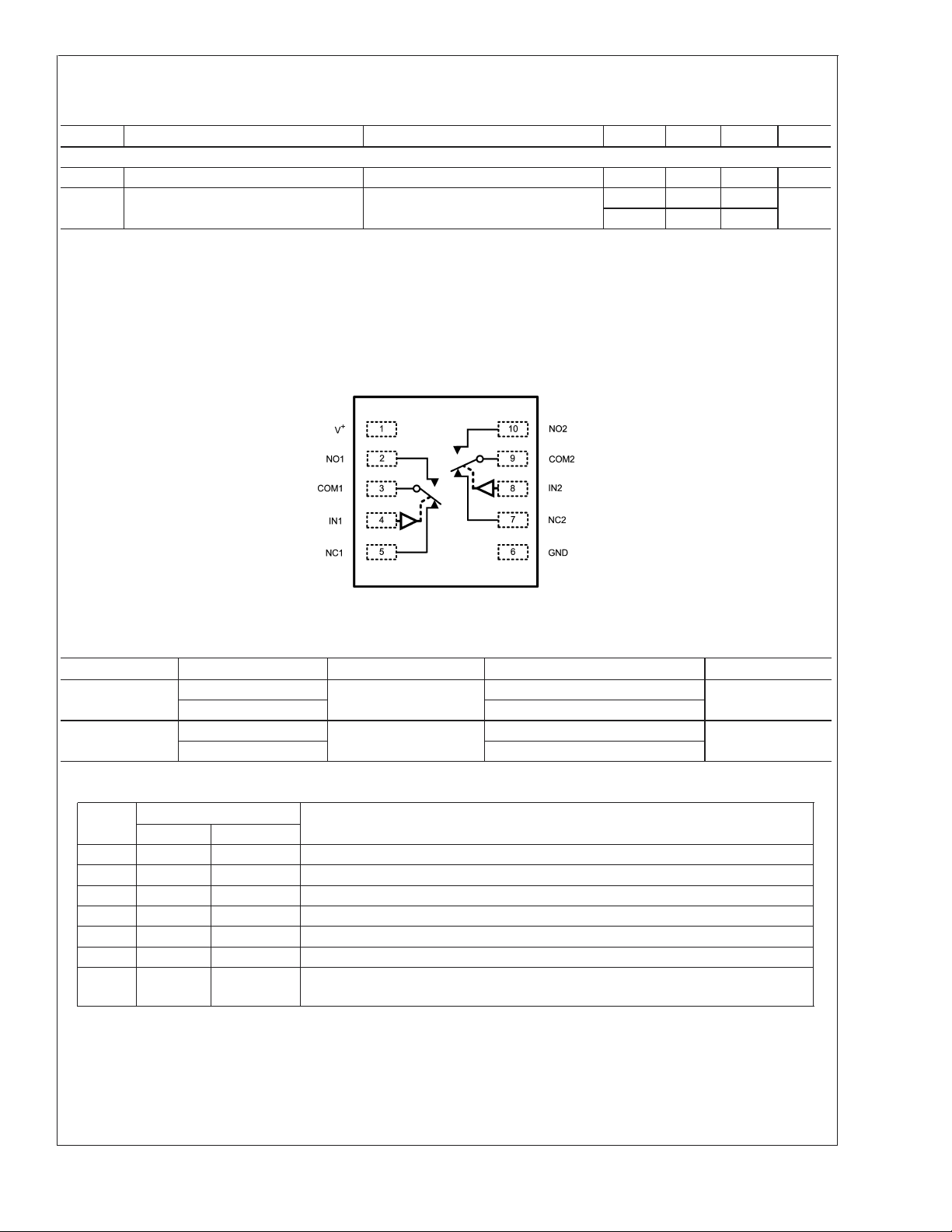
Symbolic Diagram
LMS4684
20077503
Ordering Information
Package Part Number Package Marking Transport Media NSC Drawing
12-Bump
micro SMD
10-Pin LLP LMS4684LD
LMS4684ITL
LMS4684ITLX 3k Units Tape and Reel
LMS4684LDX 4.5k Units Tape and Reel
F09A
L4684
250 Units Tape and Reel TLA12DPA
1k Units Tape and Reel LDA10B
Pin Descriptions
Name Pin ID Description
LLP micro SMD
NC 5, 7 D3, D1 Analog switch normally closed terminal
IN 4, 8 C3, C1 Digital control input
COM 3, 9 B3, B1 Analog switch common terminal
NO 2, 10 A3, A1 Analog switch normally open terminal
+
V
GND 6, GND D2 Ground
1 A2 Positive supply voltage
B2, C2 Not electrically connected. Can be used to help dissipate heat by connecting to GND
pin.
www.national.com3

Typical Performance Characteristics
LMS4684
Supply Current vs. Supply Voltage NO ON Resistance vs. COM Voltage
20077504
20077505
NC ON Resistance vs. COM Voltage Logic Threshold Voltage vs. Supply Voltage
20077506
Turn-on / Turn-off Times vs. Temperature Charge Injection vs. COM Voltage
20077508
www.national.com 4
20077507
20077509

Typical Performance Characteristics (Continued)
NC On-Resistance vs. COM Voltage NC On-Resistance vs. COM Voltage
LMS4684
20077515
NO On-Resistance vs. COM Voltage NO On-Resistance vs. COM Voltage
20077517 20077518
20077516
www.national.com5

Application Notes
PRODUCT DESCRIPTION
LMS4684
The LMS4684 is a low voltage dual analog switch with
extremely low On-Resistance operating with a supply voltage range of 1.8V to 5.5V. National has fully characterized
the LMS4684 to operate in applications with 3V nominal
supply voltage. The LMS4684 also features fast switching
times for Turn-Off (40ns max over temp) and Turn-On (65ns
max over temp).
The switch operates asymmetrically, one terminal is normally
closed (NC) and the other terminal normally open (NO).
Both NC and NO terminals are connected to a common
terminal (COM). This configuration is ideal for applications
with asymmetric loads such as speaker handsets and internal speakers.
ANALOG SIGNAL LEVELS
+
The Analog signal ranges from GND to V
and are passed
through the switch with very little change. Each switch is
bidirectional so any pin can be an input or output.
DIGITAL CONTROL INPUTS
The IN pin can be driven to 5.5V regardless of the voltage
level of the supply pin V
+
. For example if you wanted to have
a supply of 2V you could still drive the IN digital control input
to 5V. Minimum power is lost when the IN pin, is driven
rail-to-rail.
SUPPLY VOLTAGE SEQUENCING
It is good general practice to first apply the supply voltage to
a CMOS device before any other supply on other pins.This is
also true for the LMS4684 analog switch which is a CMOS
device.
However if it is necessary to have an analog signal applied
before the supply voltage is applied and the analog signal
supply is not limited to 20mA max, a diode connected between the supply voltage and the V
figure below will supply adequate input protection. This will
limit the max analog voltage to a diode drop below V
+
pin as shown in the
+
. This
diode D1 will also provide protection against some overvoltage situations.
20077519
FIGURE 1. Overvoltage Protection Circuitry
PCB LAYOUT
Both the LLP and micro SMD packages offer enhanced
board real estate savings because of their tiny footprints.
These tiny packages are capable of supporting up to an
absolute maximum of 400mA of continuous current because
of the advanced thermal handling capabilities.
The LLP package has the exposed die attach pad internally
connected to the internal circuit GND. When this pad is
soldered to copper on the PCB board according to Application Note AN-1187 the full thermal capability of the LLP
package can be achieved without additional bulky heat sinks
to dissipate the heat generated. The micro SMD package
has a similar capability to help dissipate heat generated
through Bumps B2 and C2 which are not electrically connected. To enhance heat dissipation of the micro SMD package B2 and C2 could be connected to the GND pin and
through copper traces on the board.
Please see Application Note AN-1112 for micro SMD package considerations.
www.national.com 6

Parameter Measuring Information
LMS4684
20077510
FIGURE 2. tON/t
OFF
Time
FIGURE 3. Break-Before Make Delay
20077511
FIGURE 4. Charge Injection
20077513
www.national.com7

Parameter Measuring Information (Continued)
LMS4684
FIGURE 5. Channel Capacitance
20077514
www.national.com 8

Physical Dimensions inches (millimeters) unless otherwise noted
LMS4684
10-Lead LLP
NS Package Number LDA10B
X1 = 1590±30 µm; X2 = 2327±30 µm; X3 = 600±75 µm
12-Bump micro SMD
NS Package Number TLA12DPA
www.national.com9

Notes
LMS4684 0.5Ω Low-Voltage, Dual SPDT Analog Switch
LIFE SUPPORT POLICY
NATIONAL’S PRODUCTS ARE NOT AUTHORIZED FOR USE AS CRITICAL COMPONENTS IN LIFE SUPPORT
DEVICES OR SYSTEMS WITHOUT THE EXPRESS WRITTEN APPROVAL OF THE PRESIDENT AND GENERAL
COUNSEL OF NATIONAL SEMICONDUCTOR CORPORATION. As used herein:
1. Life support devices or systems are devices or
systems which, (a) are intended for surgical implant
into the body, or (b) support or sustain life, and
whose failure to perform when properly used in
accordance with instructions for use provided in the
labeling, can be reasonably expected to result in a
significant injury to the user.
BANNED SUBSTANCE COMPLIANCE
National Semiconductor certifies that the products and packing materials meet the provisions of the Customer Products
Stewardship Specification (CSP-9-111C2) and the Banned Substances and Materials of Interest Specification
(CSP-9-111S2) and contain no ‘‘Banned Substances’’ as defined in CSP-9-111S2.
National Semiconductor
Americas Customer
Support Center
Email: new.feedback@nsc.com
Tel: 1-800-272-9959
www.national.com
National Semiconductor
Europe Customer Support Center
Fax: +49 (0) 180-530 85 86
Email: europe.support@nsc.com
Deutsch Tel: +49 (0) 69 9508 6208
English Tel: +44 (0) 870 24 0 2171
Français Tel: +33 (0) 1 41 91 8790
2. A critical component is any component of a life
support device or system whose failure to perform
can be reasonably expected to cause the failure of
the life support device or system, or to affect its
safety or effectiveness.
National Semiconductor
Asia Pacific Customer
Support Center
Email: ap.support@nsc.com
National Semiconductor
Japan Customer Support Center
Fax: 81-3-5639-7507
Email: jpn.feedback@nsc.com
Tel: 81-3-5639-7560
National does not assume any responsibility for use of any circuitry described, no circuit patent licenses are implied and National reserves the right at any time without notice to change said circuitry and specifications.
 Loading...