

March 14, 2008
LMP7721
3 Femtoampere Input Bias Current Precision Amplifier
LMP7721 3 Femtoampere Input Bias Current Precision Amplifier
General Description
The LMP7721 is the industry’s lowest guaranteed input bias
current precision amplifier. The ultra low input bias current is
3 fA, with a guaranteed limit of ±20 fA at 25°C and ±900 fA at
85°C. This is achieved with the latest patent pending technology of input bias current cancellation amplifier circuitry.
This technology also maintains the ultra low input bias current
over the entire input common mode voltage range of the amplifier.
Other outstanding features, such as low voltage noise (6.5
), low DC offset voltage (±150 µV maximum at 25°C)
nV/
and low offset voltage temperature coefficient (−1.5 µV/°C),
improve system sensitivity and accuracy in high precision applications. With a supply voltage range of 1.8V to 5.5V, the
LMP7721 is the ideal choice for battery operated portable applications. The LMP7721 is part of the LMP® precision amplifier family.
As part of National’s PowerWise® products, the LMP7721
provides the remarkably wide gain bandwidth product (GBW)
of 17 MHz while consuming only 1.3 mA of current. This wide
GBW along with the high open loop gain of 120 dB enables
accurate signal conditioning. With these specifications, the
LMP7721 has the performance to excel in a wide variety of
applications such as electrochemical cell amplifiers and sensor interface circuits.
The LMP7721 is offered in an 8-pin SOIC package with a
special pinout that isolates the amplifier’s input from the power supply and output pins. With proper board layout techniques, the unique pinout of the LMP7721 will prevent PCB
leakage current from reaching the input pins. Thus system
error will be further reduced.
Features
Unless otherwise noted, typical values at TA = 25°C, VS = 5V.
Input bias current (VCM = 1V)
■
max @ 25°C ±20 fA
—
max @ 85°C ±900 fA
—
Offset voltage ±26 µV
■
Offset voltage drift
■
DC Open loop gain 120 dB
■
DC CMRR 100 dB
■
Input voltage noise (at f = 1 kHz) 6.5 nV/√Hz
■
THD 0.0007%
■
Supply current 1.3 mA
■
GBW 17 MHz
■
Slew rate (falling edge) 12.76 V/μs
■
Supply voltage 1.8V to 5.5V
■
Operating temperature range −40°C to 125°C
■
8-Pin SOIC
■
−1.5 μV/°C
Applications
Photodiode amplifier
■
High impedance sensor amplifier
■
Ion chamber amplifier
■
Electrometer amplifier
■
pH electrode amplifier
■
Transimpedance amplifier
■
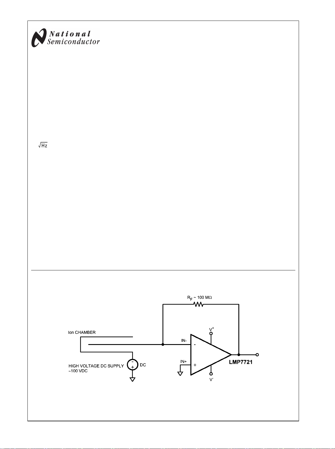
Block Diagram of a Typical Application
Ion Chamber: Current to Voltage Converter
LMP® is a registered trademark of National Semiconductor Corporation.
PowerWise® is a registered trademark of National Semiconductor.
© 2008 National Semiconductor Corporation 202040 www.national.com
20204084
Absolute Maximum Ratings (Note 1)
If Military/Aerospace specified devices are required,
please contact the National Semiconductor Sales Office/
LMP7721
Soldering Information
Infrared or Convection (20 sec) 235°C
Wave Soldering Lead Temp. (10 sec) 260°C
Distributors for availability and specifications.
ESD Tolerance (Note 2)
Human Body Model 2000V
Machine Model 200V
VIN Differential
Supply Voltage (VS = V+ – V−) (Note 10)
±0.3V
6.0V
Voltage on Input/Output Pins V+ +0.3V, V− −0.3V
Storage Temperature Range −65°C to 150°C
Operating Ratings (Note 1)
Temperature Range (Note 3) −40°C to 125°C
Supply Voltage (VS = V+ – V−)
0°C ≤ TA ≤ 125°C
−40°C ≤ TA ≤ 125°C
Package Thermal Resistance (θJA(Note 3))
8-Pin SOIC 190°C/W
Junction Temperature (Note 3) +150°C
2.5V Electrical Characteristics
Unless otherwise specified, all limits are guaranteed for TA = 25°C, V+ = 2.5V, V− = 0V, VCM = (V+ + V−)/2. Boldface limits apply
at the temperature extremes.
Symbol Parameter Conditions Min
(Note 5)
V
OS
TC VOSInput Offset Voltage Drift
Input Offset Voltage ±50 ±180
–1.5 –4
(Note 6)
I
BIAS
Input Bias Current VCM = 1V
(Notes 7, 8)
25°C ±3 ±20
−40°C to 85°C ±900
−40°C to 125°C ±5 pA
I
OS
Input Offset Current VCM = 1V
(Note 8)
CMRR Common Mode Rejection Ratio
0V ≤ VCM ≤ 1.4V
83
80
PSRR Power Supply Rejection Ratio
CMVR Input Common-Mode Voltage
Range
A
VOL
V
O
Large Signal Voltage Gain VO = 0.15V to 2.2V
Output Swing High
1.8V ≤ V+ ≤ 5.5V
V− = 0V, VCM = 0
CMRR ≥ 80 dB
CMRR ≥ 78 dB
RL = 2 kΩ to V+/2
VO = 0.15V to 2.2V
RL = 10 kΩ to V+/2
RL = 2 kΩ to V+/2
84
80
−0.3
–0.3
88
82
92
88
70
77
RL = 10 kΩ to V+/2
60
66
Output Swing Low
RL = 2 kΩ to V+/2
RL = 10 kΩ to V+/2
I
O
Output Short Circuit Current Sourcing to V
VIN = 200 mV (Note 9)
Sinking to V
VIN = −200 mV (Note 9)
I
S
Supply Current 1.1 1.5
−
36
30
+
7.5
5.0
SR Slew Rate AV = +1, Rising (10% to 90%)
AV = +1, Falling (90% to 10%)
6 40 fA
30 70
15 60
Typ
(Note 4)
100
92
1.5
107
120
25
20
46
15
9.3
10.8
Max
(Note 5)
±480
1.5
73
62
1.75
1.8V to 5.5V
2.0V to 5.5V
Units
μV
μV/°C
fA
dB
dB
V
dB
mV
from V
mV
mA
mA
V/μs
+
www.national.com 2
LMP7721
Symbol Parameter Conditions Min
(Note 5)
Typ
(Note 4)
Max
(Note 5)
Units
GBW Gain Bandwidth Product 15 MHz
e
n
i
n
THD+N Total Harmonic Distortion + Noise
Input-Referred Voltage Noise f = 400 Hz 8
f = 1 kHz 7
Input-Referred Current Noise f = 1 kHz 0.01
f = 1 kHz, AV = 2, RL = 100 kΩ
VO = 0.9 V
PP
f = 1 kHz, AV = 2, RL = 600Ω
VO = 0.9 V
PP
0.003
0.003
nV/
pA/
%
5V Electrical Characteristics
Unless otherwise specified, all limits are guaranteed for TA = 25°C, V+ = 5V, V− = 0V, VCM = (V+ + V−)/2. Boldface limits apply at
the temperature extremes.
Symbol Parameter Conditions Min
(Note 5)
V
OS
TC VOSInput Offset Average Drift
Input Offset Voltage ±26 ±150
–1.5 –4
(Note 6)
I
BIAS
Input Bias Current VCM = 1V
(Notes 7, 8)
25°C ±3 ±20
−40°C to 85°C ±900
−40°C to 125°C ±5 pA
I
OS
CMRR Common Mode Rejection Ratio
Input Offset Current (Note 8) 6 40 fA
0V ≤ VCM ≤ 3.7V
84
82
PSRR Power Supply Rejection Ratio
CMVR Input Common-Mode Voltage
Range
A
VOL
V
O
Large Signal Voltage Gain VO = 0.3V to 4.7V
Output Swing High
1.8V ≤ V+ ≤ 5.5V
V− = 0V, VCM = 0
CMRR ≥ 80 dB
CMRR ≥ 78 dB
RL = 2 kΩ to V+/2
VO = 0.3V to 4.7V
RL = 10 kΩ to V+/2
RL = 2 kΩ to V+/2
84
80
−0.3
–0.3
88
82
92
88
70
77
RL = 10 kΩ to V+/2
60
66
Output Swing Low
RL = 2 kΩ to V+/2
RL = 10 kΩ to V+/2
I
O
Output Short Circuit Current Sourcing to V
−
VIN = 200 mV (Note 9)
Sinking to V
+
VIN = −200 mV (Note 9)
I
S
Supply Current 1.3 1.7
31 70
20 60
46
38
10.5
6.5
SR Slew Rate AV = +1, Rising (10% to 90%) 10.43
AV = +1, Falling (90% to 10%)
GBW Gain Bandwidth Product 17 MHz
Typ
(Note 4)
100
96
4
111
120
30
20
60
22
12.76
Max
(Note 5)
±450
4
73
62
1.95
Units
μV
μV/°C
fA
dB
dB
V
dB
mV
from V
mV
mA
mA
V/μs
+
3 www.national.com
Symbol Parameter Conditions Min
e
n
LMP7721
Input-Referred Voltage Noise f = 400 Hz 7.5
(Note 5)
Typ
(Note 4)
Max
(Note 5)
f = 1 kHz 6.5
i
n
THD+N Total Harmonic Distortion +
Note 1: Absolute Maximum Ratings indicate limits beyond which damage to the device may occur. Operating Ratings indicate conditions for which the device is
intended to be functional, but specific performance is not guaranteed. For guaranteed specifications and the test conditions, see the Electrical Characteristics
Tables.
Note 2: Human Body Model, applicable std. MIL-STD-883, Method 3015.7. Machine Model, applicable std. JESD22-A115-A (ESD MM std. of JEDEC)
Field-Induced Charge-Device Model, applicable std. JESD22-C101-C (ESD FICDM std. of JEDEC).
Note 3: The maximum power dissipation is a function of T
PD = (T
Note 4: Typical values represent the most likely parametric norm as determined at the time of characterization. Actual typical values may vary over time and will
also depend on the application and configuration. The typical values are not tested and are not guaranteed on shipped production material.
Note 5: Limits are 100% production tested at 25°C. Limits over the operating temperature range are guaranteed through correlations using the Statistical Quality
Control (SQC) method.
Note 6: Offset voltage average drift is determined by dividing the change in VOS at the temperature extremes by the total temperature change.
Note 7: Positive current corresponds to current flowing into the device.
Note 8: This parameter is guaranteed by design and/or characterization and is not tested in production.
Note 9: The short circuit test is a momentary open loop test.
Note 10: The voltage on any pin should not exceed 6V relative to any other pins.
Input-Referred Current Noise f = 1 kHz 0.01
f = 1 kHz, AV = 2, RL = 100 kΩ
Noise
VO = 4 V
PP
f = 1 kHz, AV = 2, RL = 600Ω
VO = 4 V
- TA)/θJA. All numbers apply for packages soldered directly onto a PC Board.
J(MAX)
PP
, θJA. The maximum allowable power dissipation at any ambient temperature is
J(MAX)
0.0007
0.0007
Units
nV/
pA/
%
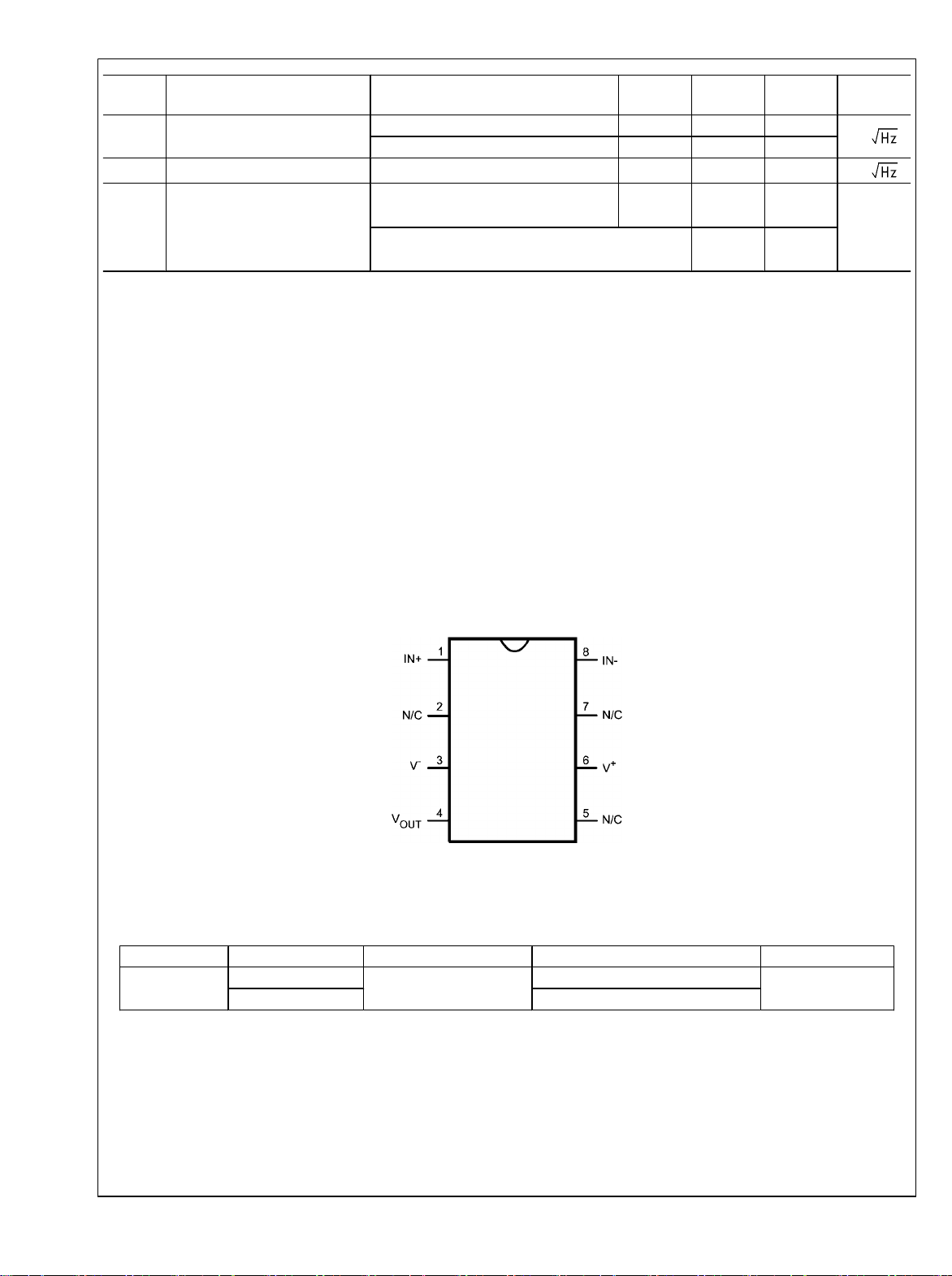
Connection Diagram
8-Pin SOIC
Top View
20204083
Ordering Information
Package Part Number Package Marking Transport Media NSC Drawing
8-Pin SOIC
LMP7721MA
LMP7721MAX 2.5k Units Tape and Reel
LMP7721MA
95 Units/Rail
M08A
www.national.com 4
LMP7721
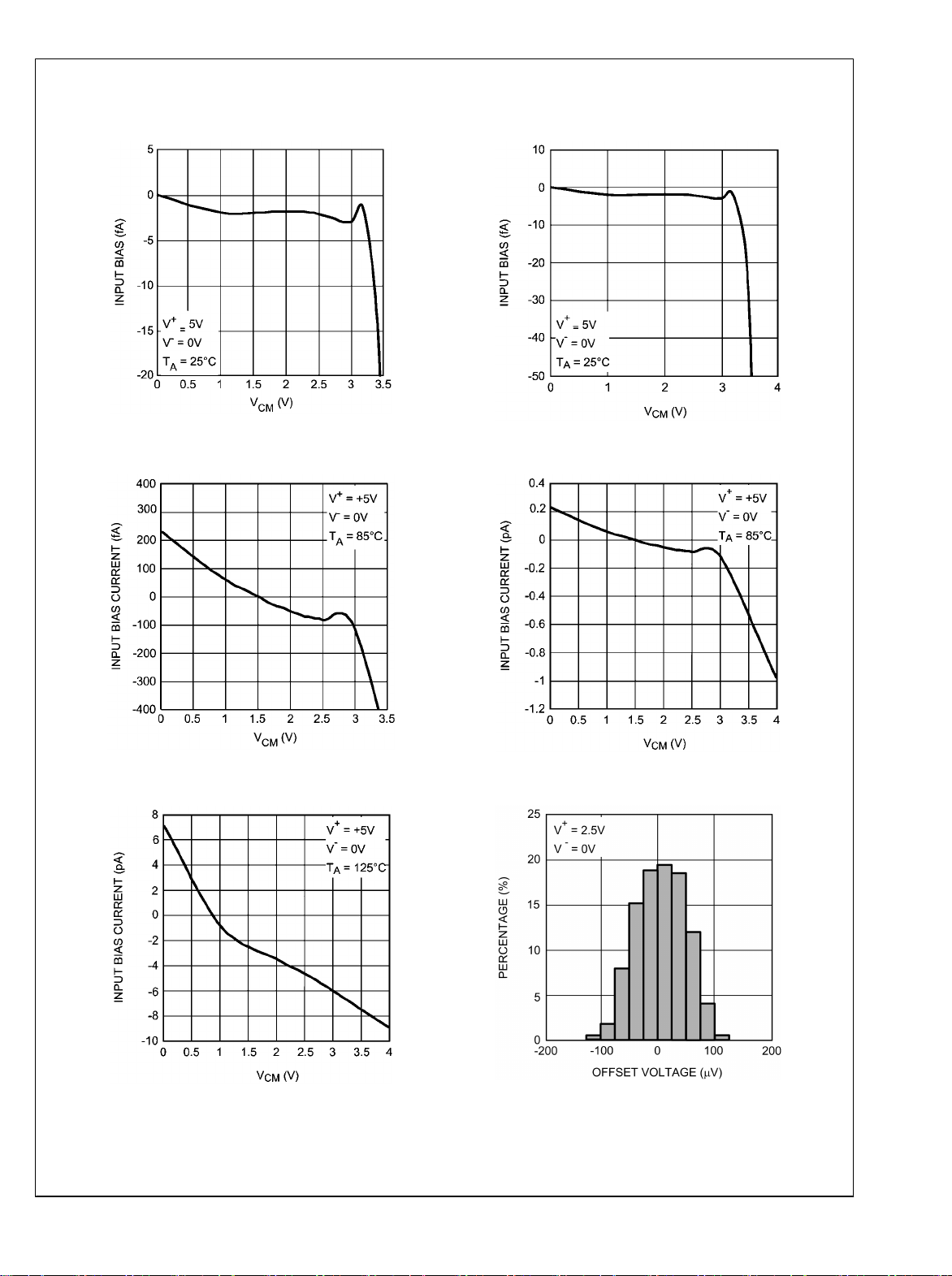
Typical Performance Characteristics Unless otherwise specified: T
Input Bias Current vs. V
Input Bias Current vs. V
CM
20204094
CM
Input Bias Current vs. V
Input Bias Current vs. V
= 25°C, VCM = (V+ + V−)/2.
A
CM
20204087
CM
Input Bias Current vs. V
CM
20204095
20204085
20204086
Offset Voltage Distribution
20204039
5 www.national.com
 Loading...