

查询LMP7718MME供应商
LMP7717/LMP7718
88 MHz, Precision, Low Noise, 1.8V CMOS Input,
Decompensated Operational Amplifier
November 6, 2007
LMP7717/LMP7718 88 MHz, Precision, Low Noise, 1.8V CMOS Input, Decompensated
Operational Amplifier
General Description
The LMP7717 (single) and the LMP7718 (dual) low noise,
CMOS input operational amplifiers offer a low input voltage
noise density of 5.8 nV/
(LMP7717) of quiescent current. The LMP7717/LMP7718 are
stable at a gain of 10 and have a gain bandwidth (GBW)
product of 88 MHz. The LMP7717/LMP7718 have a supply
voltage range of 1.8V to 5.5V and can operate from a single
supply. The LMP7717/LMP7718 each feature a rail-to-rail
output stage. Both amplifiers are part of the LMP® precision
amplifier family and are ideal for a variety of instrumentation
applications.
The LMP7717 family provides optimal performance in low
voltage and low noise systems. A CMOS input stage, with
typical input bias currents in the range of a few femto-Amperes, and an input common mode voltage range, which
includes ground, make the LMP7717/LMP7718 ideal for low
power sensor applications where high speeds are needed.
The LMP7717/LMP7718 are manufactured using National’s
advanced VIP50 process. The LMP7717 is offered in either a
5-Pin SOT23 or an 8-Pin SOIC package. The LMP7718 is
offered in either the 8-Pin SOIC or the 8-Pin MSOP.
while consuming only 1.15 mA
Features
(Typical 5V supply, unless otherwise noted)
Input offset voltage ±150 µV (max)
■
Input referred voltage noise 5.8 nV/√Hz
■
Input bias current 100 fA
■
Gain bandwidth product 88 MHz
■
Supply voltage range 1.8V to 5.5V
■
Supply current per channel
■
LMP7717 1.15 mA
—
LMP7718 1.30 mA
—
Rail-to-Rail output swing
■
@ 10 kΩ load 25 mV from rail
—
@ 2 kΩ load 45 mV from rail
—
Guaranteed 2.5V and 5.0V performance
■
Total harmonic distortion 0.04% @1 kHz, 600Ω
■
Temperature range −40°C to 125°C
■
Applications
ADC interface
■
Photodiode amplifiers
■
Active filters and buffers
■
Low noise signal processing
■
Medical instrumentation
■
Sensor interface applications
■
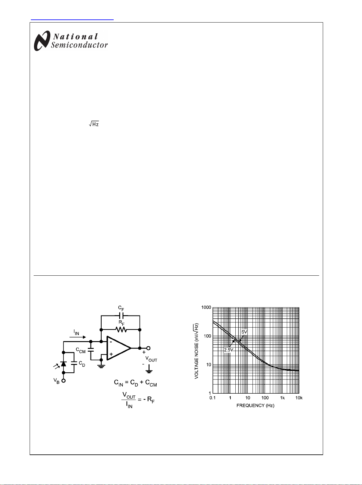
Typical Application
Photodiode Transimpedance Amplifier
LMP® is a registered trademark of National Semiconductor Corporation.
© 2007 National Semiconductor Corporation 300108 www.national.com
30010869
Input Referred Voltage Noise vs. Frequency
30010839

Absolute Maximum Ratings (Note 1)
If Military/Aerospace specified devices are required,
please contact the National Semiconductor Sales Office/
Distributors for availability and specifications.
ESD Tolerance (Note 2)
Human Body Model 2000V
LMP7717/LMP7718
Machine Model 200V
VIN Differential
Supply Voltage (V+ – V−)
Input/Output Pin Voltage V+ +0.3V, V− −0.3V
Storage Temperature Range −65°C to 150°C
Junction Temperature (Note 3) +150°C
±0.3V
6.0V
Soldering Information
Infrared or Convection (20 sec) 235°C
Wave Soldering Lead Temp (10 sec) 260°C
Operating Ratings (Note 1)
Temperature Range (Note 3) −40°C to 125°C
Supply Voltage (V+ – V−)
−40°C ≤ TA ≤ 125°C
0°C ≤ TA ≤ 125°C
Package Thermal Resistance (θJA (Note 3))
5-Pin SOT23 180°C/W
8-Pin SOIC 190°C/W
8-Pin MSOP 236°C/W
2.5V Electrical Characteristics (Note 4)
Unless otherwise specified, all limits are guaranteed for TA = 25°C, V+ = 2.5V, V− = 0V, VCM = V+/2 = VO. Boldface limits apply at
the temperature extremes.
Symbol Parameter Conditions Min
(Note 6)
V
OS
TC VOSInput Offset Average Drift
I
B
I
OS
CMRR Common Mode Rejection Ratio
PSRR Power Supply Rejection Ratio
CMVR Input Common-Mode Voltage
A
VOL
V
OUT
Input Offset Voltage ±20 ±180
LMP7717 −1.0
(Note 7)
Input Bias Current VCM = 1.0V
Input Offset Current VCM = 1.0V
Range
Open Loop Gain V
Output Swing High
Output Swing Low
LMP7718 −1.8
−40°C ≤ TA ≤ 85°C
(Notes 8, 9)
−40°C ≤ TA ≤ 125°C
(Note 9)
0V ≤ VCM ≤ 1.4V
2.0V ≤ V+ ≤ 5.5V, VCM = 0V
1.8V ≤ V+ ≤ 5.5V, VCM = 0V
CMRR ≥ 60 dB
CMRR ≥ 55 dB
= 0.15V to 2.2V,
OUT
RL = 2 kΩ to V+/2
V
= 0.15V to 2.2V,
OUT
RL = 10 kΩ to V+/2
RL = 2 kΩ to V+/2
RL = 10 kΩ to V+/2
RL = 2 kΩ to V+/2
RL = 10 kΩ to V+/2
LMP7717 88
LMP7718 84
LMP7717 92
LMP7718 90
83
80
85
80
85 98
−0.3
−0.3
82
80
88
86
0.05 1
0.05 1
.006 0.5
25 70
20 60
30 70
15 60
Typ
(Note 5)
94
100
1.5
98
92
110
95
Max
(Note 6)
±480
±4
25
100
50
1.5
77
66
73
62
2.0V to 5.5V
1.8V to 5.5V
Units
µV
μV/°C
pA
pA
dB
dB
V
dB
mV from
rail
www.national.com 2

LMP7717/LMP7718
I
OUT
I
S
Output Short Circuit Current Sourcing to V
VIN = 200 mV (Note 10)
Sinking to V
VIN = –200 mV (Note 10)
Supply Current per Amplifier LMP7717 0.95 1.30
−
36
47
30
+
7.5
15
5
1.65
LMP7718 per channel 1.1 1.5
1.85
SR Slew Rate AV = +10, Rising (10% to 90%)
AV = +10, Falling (90% to 10%)
GBWP Gain Bandwidth Product
e
n
i
n
Input-Referred Voltage Noise f = 1 kHz 6.2
Input-Referred Current Noise f = 1 kHz 0.01
THD+N Total Harmonic Distortion +
AV = +10, RL = 10 kΩ
f = 1 kHz, AV = 1, RL = 600Ω
0.01 %
32
24
88 MHz
Noise
5V Electrical Characteristics (Note 4)
Unless otherwise specified, all limits are guaranteed for TA = 25°C, V+ = 5V, V− = 0V, VCM = V+/2 = VO. Boldface limits apply at
the temperature extremes.
Symbol Parameter Conditions Min
(Note 6)
V
OS
TC VOSInput Offset Average Drift
I
B
Input Offset Voltage ±10 ±150
LMP7717 −1.0
(Note 7)
Input Bias Current VCM = 2.0V
LMP7718 −1.8
−40°C ≤ TA ≤ 85°C
(Notes 8, 9)
−40°C ≤ TA ≤ 125°C
I
OS
Input Offset Current VCM = 2.0V
(Note 9)
CMRR Common Mode Rejection Ratio
0V ≤ VCM ≤ 3.7V
85
80
PSRR Power Supply Rejection Ratio
2.0V ≤ V+ ≤ 5.5V, VCM = 0V
85
80
85 98
−0.3
−0.3
82
CMVR Input Common-Mode Voltage
Range
A
VOL
Open Loop Gain V
1.8V ≤ V+ ≤ 5.5V, VCM = 0V
CMRR ≥ 60 dB
CMRR ≥ 55 dB
= 0.3V to 4.7V,
OUT
RL = 2 kΩ to V+/2
LMP7717 88
LMP7718 84
80
V
= 0.3V to 4.7V,
OUT
RL = 10 kΩ to V+/2
LMP7717 92
88
LMP7718 90
86
0.1 1
0.1 1
.01 0.5
Typ
(Note 5)
100
100
4
107
90
110
95
Max
(Note 6)
±450
±4
25
100
50
4
mA
mA
V/μs
nV/
pA/
Units
µV
μV/°C
pA
pA
dB
dB
V
dB
3 www.national.com

V
OUT
Output Swing High
RL = 2 kΩ to V+/2
LMP7717 35 70
LMP7718 45 80
25 60
LMP7717/LMP7718
Output Swing Low
RL = 10 kΩ to V+/2
RL = 2 kΩ to V+/2
LMP7717 42 70
LMP7718 50 80
25 60
46
60
38
10.5
21
6.5
I
OUT
I
S
RL = 10 kΩ to V+/2
Output Short Circuit Current Sourcing to V
−
VIN = 200 mV (Note 10)
Sinking to V
+
VIN = –200 mV (Note 10)
Supply Current per Amplifier LMP7717 1.15 1.40
LMP7718 per channel 1.30 1.70
SR Slew Rate AV = +10, Rising (10% to 90%) 35
AV = +10, Falling (90% to 10%) 28
GBWP Gain Bandwidth Product
e
n
i
n
Input-Referred Voltage Noise f = 1 kHz 5.8
Input-Referred Current Noise f = 1 kHz 0.01
THD+N Total Harmonic Distortion +
AV = +10, RL = 10 kΩ
f = 1 kHz, AV = 1, RL = 600Ω
88 MHz
0.01 %
Noise
77
77
66
73
78
66
1.75
2.05
mV from
rail
mA
mA
V/μs
nV/
pA/
Note 1: Absolute Maximum Ratings indicate limits beyond which damage to the device may occur. Operating Ratings indicate conditions for which the device is
intended to be functional, but specific performance is not guaranteed. For guaranteed specifications and the test conditions, see the Electrical Characteristics
Tables.
Note 2: Human Body Model, applicable std. MIL-STD-883, Method 3015.7. Machine Model, applicable std. JESD22-A115-A (ESD MM std. of JEDEC)
Field-Induced Charge-Device Model, applicable std. JESD22-C101-C (ESD FICDM std. of JEDEC).
Note 3: The maximum power dissipation is a function of T
PD = (T
Note 4: Electrical Table values apply only for factory testing conditions at the temperature indicated. Factory testing conditions result in very limited self-heating
of the device such that TJ = TA. No guarantee of parametric performance is indicated in the electrical tables under conditions of internal self-heating where TJ >
TA.
Note 5: Typical values represent the most likely parametric norm as determined at the time of characterization. Actual typical values may vary over time and will
also depend on the application and configuration. The typical values are not tested and are not guaranteed on shipped production material.
Note 6: Limits are 100% production tested at 25°C. Limits over the operating temperature range are guaranteed through correlations using the statistical quality
control (SQC) method.
Note 7: Offset voltage average drift is determined by dividing the change in VOS by temperature change.
Note 8: Positive current corresponds to current flowing into the device.
Note 9: Input bias current and input offset current are guaranteed by design
Note 10: The short circuit test is a momentary test, the short circuit duration is 1.5 ms.
- TA)/θJA. All numbers apply for packages soldered directly onto a PC Board.
J(MAX)
, θJA. The maximum allowable power dissipation at any ambient temperature is
J(MAX)
www.national.com 4
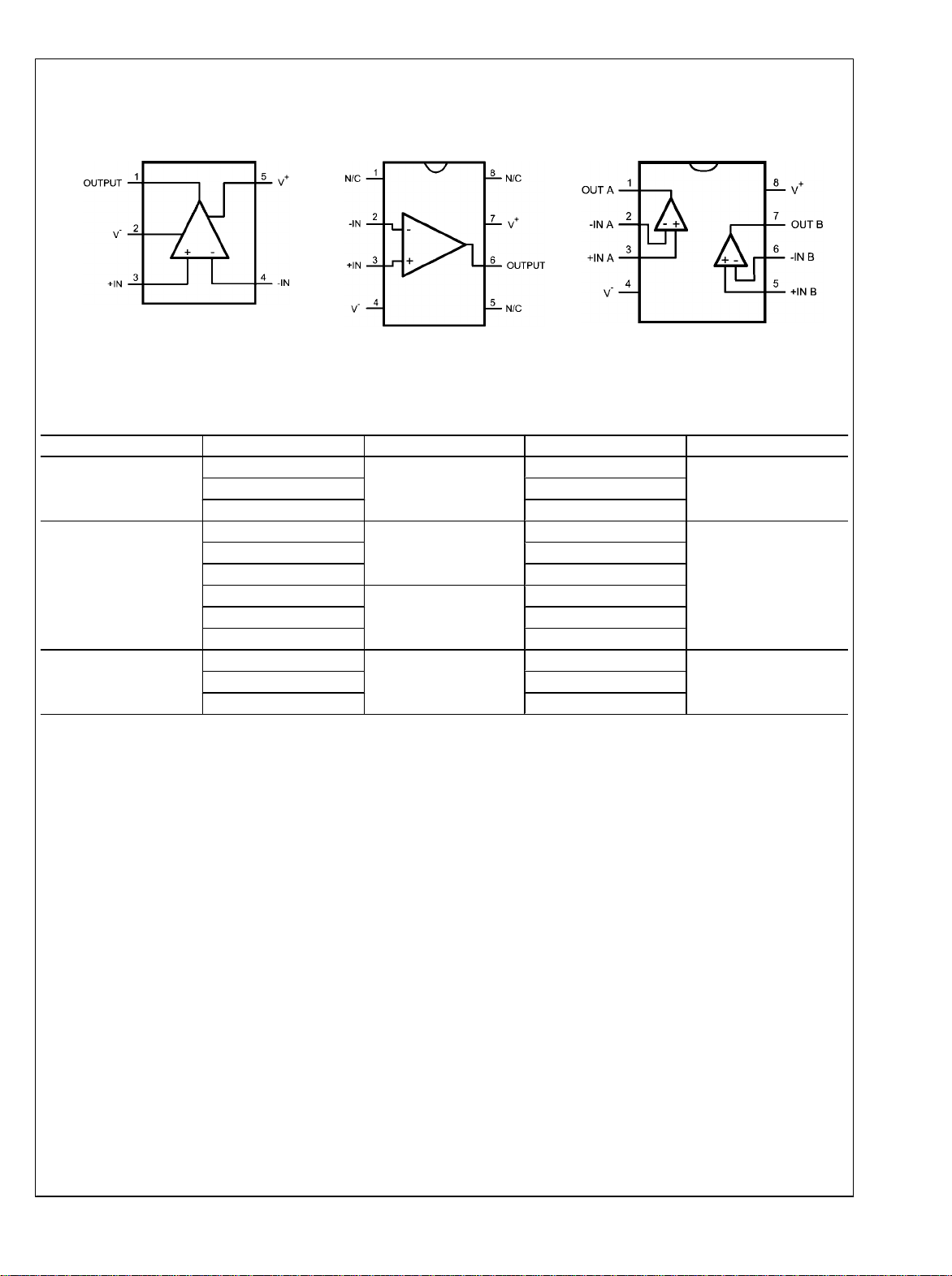
Connection Diagrams
LMP7717/LMP7718
5-Pin SOT23 (LMP7717)
Top View
30010801
8-Pin SOIC (LMP7717)
Top View
8-Pin SOIC/MSOP (LMP7718)
30010885
Ordering Information
Package Part Number Package Marking Transport Media NSC Drawing
5-Pin SOT23
8-Pin SOIC
8-Pin MSOP
LMP7717MF
AT4A
LMP7717MFX 3k Units Tape and Reel
LMP7717MA
LMP7717MAE 250 Units Tape and Reel
LMP7717MAX 2.5k Units Tape and Reel
LMP7718MA
LMP7718MAE 250 Units Tape and Reel
LMP7718MAX 2.5k Units Tape and Reel
LMP7718MM
LMP7718MMX 3.5k Units Tape and Reel
LMP7717MA
LMP7718MA
AP4A
1k Units Tape and Reel
95 Units/Rail
95 Units/Rail
1k Units Tape and Reel
30010802
MF05ALMP7717MFE 250 Units Tape and Reel
M08A
MUA08ALMP7718MME 250 Units Tape and Reel
5 www.national.com

Typical Performance Characteristics Unless otherwise specified, T
VS = V+ - V−, VCM = VS/2.
= 25°C, V– = 0, V+ = 5V,
A
TCVOS Distribution (LMP7717)
LMP7717/LMP7718
TCVOS Distribution (LMP7717)
30010890
Offset Voltage Distribution
30010891
Offset Voltage Distribution
30010892
Supply Current vs. Supply Voltage (LMP7717)
30010805
www.national.com 6
VOS vs. V
30010893
CM
30010809

LMP7717/LMP7718
VOS vs. V
CM
VOS vs. Supply Voltage
30010851
VOS vs. V
CM
Slew Rate vs. Supply Voltage
30010811
Input Bias Current vs. V
CM
30010812
30010862
Input Bias Current vs. V
30010852
CM
30010887
7 www.national.com
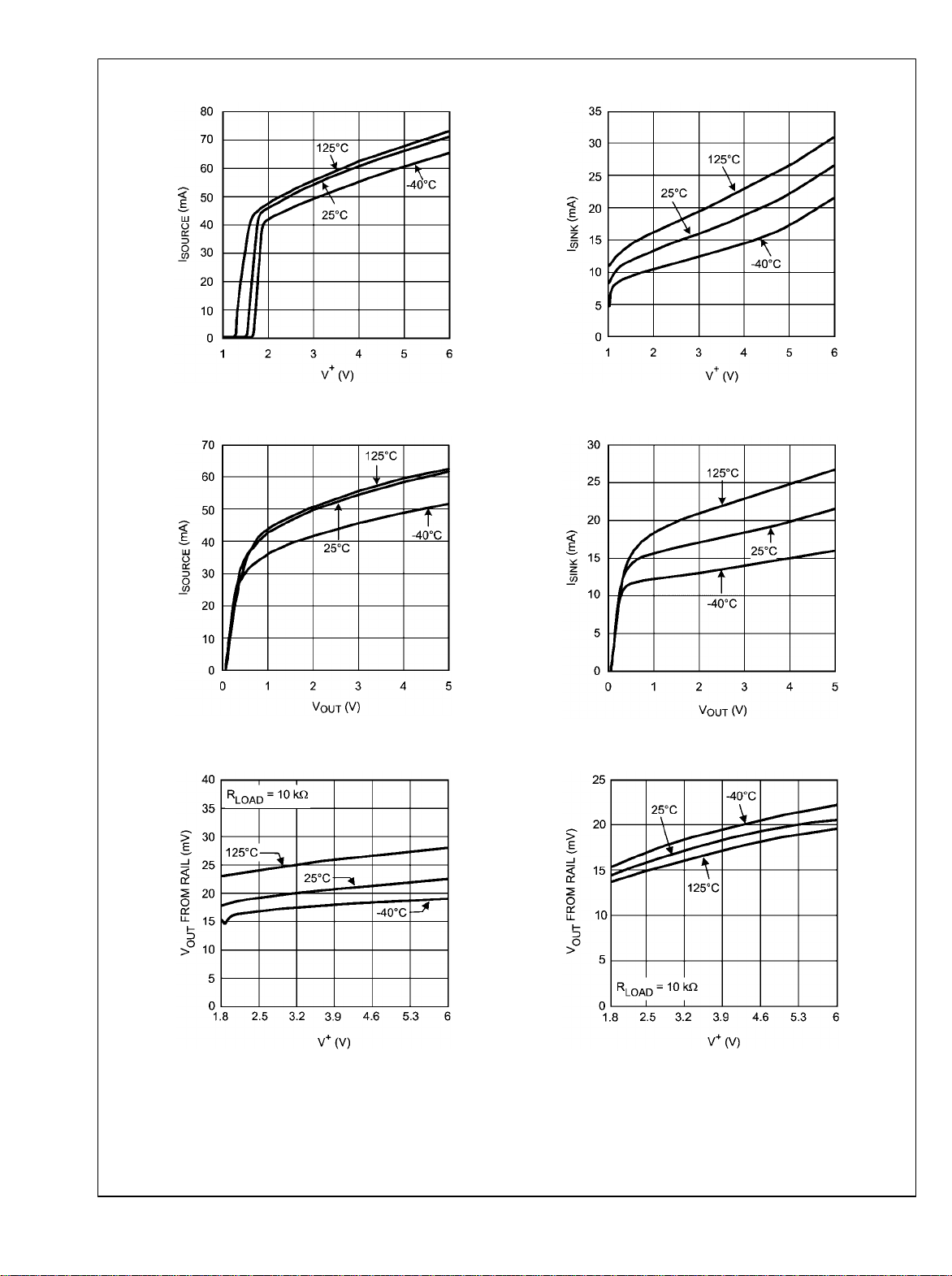
Sourcing Current vs. Supply Voltage
LMP7717/LMP7718
Sinking Current vs. Supply Voltage
30010820
Sourcing Current vs. Output Voltage
30010850
Positive Output Swing vs. Supply Voltage
30010819
Sinking Current vs. Output Voltage
30010854
Negative Output Swing vs. Supply Voltage
30010817
www.national.com 8
30010815
 Loading...