


LMK03000 Family
Precision Clock Conditioner with Integrated VCO
LMK03000 Family Precision Clock Conditioner with Integrated VCO
September 4, 2008
General Description
The LMK03000 family of precision clock conditioners combine the functions of jitter cleaning/reconditioning, multiplication, and distribution of a reference clock. The devices
integrate a Voltage Controlled Oscillator (VCO), a high performance Integer-N Phase Locked Loop (PLL), a partially
integrated loop filter, and up to eight outputs in various LVDS
and LVPECL combinations.
The VCO output is optionally accessible on the Fout port. Internally, the VCO output goes through a VCO Divider to feed
the various clock distribution blocks.
Each clock distribution block includes a programmable divider, a phase synchronization circuit, a programmable delay,
a clock output mux, and an LVDS or LVPECL output buffer.
This allows multiple integer-related and phase-adjusted
copies of the reference to be distributed to eight system components.
The clock conditioners come in a 48-pin LLP package and are
footprint compatible with other clocking devices in the same
family.
Target Applications
Data Converter Clocking
■
Networking, SONET/SDH, DSLAM
■
Wireless Infrastructure
■
Medical
■
Test and Measurement
■
Military / Aerospace
■
Features
Integrated VCO with very low phase noise floor
■
Integrated Integer-N PLL with outstanding normalized
■
phase noise contribution of -224 dBc/Hz
VCO divider values of 2 to 8 (all divides)
■
Channel divider values of 1, 2 to 510 (even divides)
■
LVDS and LVPECL clock outputs
■
Partially integrated loop filter
■
Dedicated divider and delay blocks on each clock output
■
Pin compatible family of clocking devices
■
3.15 to 3.45 V operation
■
Package: 48 pin LLP (7.0 x 7.0 x 0.8 mm)
■
200 fs RMS Clock generator performance (10 Hz to 20
■
MHz) with a clean input clock
VCO
Device Outputs
LMK03000C
LMK03000 800
LMK03000D 1200
LMK03001C
LMK03001 800
LMK03001D 1200
LMK03033C
LMK03033 800
3 LVDS
5 LVPECL
4 LVDS
4 LVPECL
Tuning Range
(MHz)
1185 - 1296
1470 - 1570
1843 - 2160
RMS Jitter
(fs)
400
400
500
System Diagram
20211440
TRI-STATE® is a registered trademark of National Semiconductor Corporation.
© 2008 National Semiconductor Corporation 202114 www.national.com
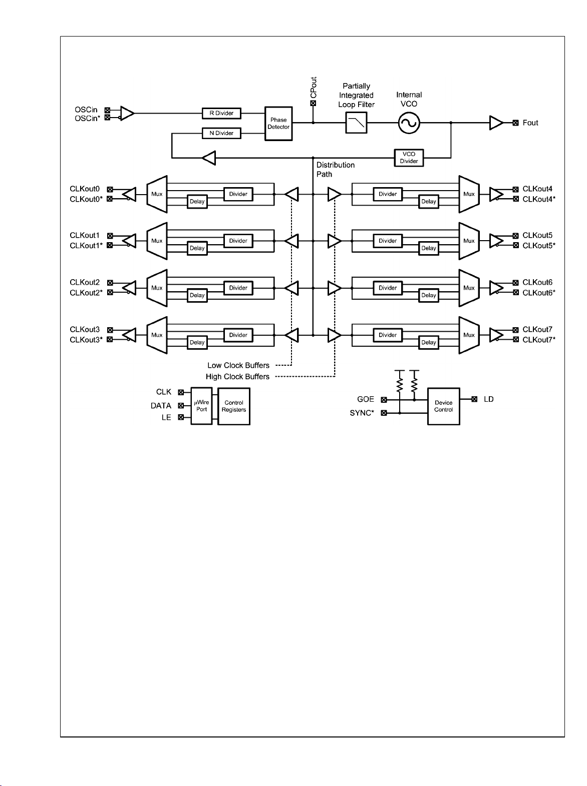
Functional Block Diagram
LMK03000 Family
20211401
www.national.com 2

Connection Diagram
LMK03000 Family
48-Pin LLP Package
20211402
3 www.national.com

Pin Descriptions
Pin # Pin Name I/O Description
1, 25 GND - Ground
2 Fout O Internal VCO Frequency Output
3, 8, 13, 16, 19, 22,
LMK03000 Family
26, 30, 31, 33, 37,
40, 43, 46
4 CLKuWire I MICROWIRE Clock Input
5 DATAuWire I MICROWIRE Data Input
6 LEuWire I MICROWIRE Latch Enable Input
7, 34, 35 NC - No Connection to these pins
9, 10 LDObyp1, LDObyp2 - LDO Bypass
11 GOE I Global Output Enable
12 LD O Lock Detect and Test Output
14, 15 CLKout0, CLKout0* O LVDS Clock Output 0
17, 18 CLKout1, CLKout1* O LVDS Clock Output 1
20, 21 CLKout2, CLKout2* O LVDS Clock Output 2
23, 24 CLKout3, CLKout3* O
27 SYNC* I Global Clock Output Synchronization
28, 29 OSCin, OSCin* I
32 CPout O Charge Pump Output
36 Bias I Bias Bypass
38, 39 CLKout4, CLKout4* O LVPECL Clock Output 4
41, 42 CLKout5, CLKout5* O LVPECL Clock Output 5
44, 45 CLKout6, CLKout6* O LVPECL Clock Output 6
47, 48 CLKout7, CLKout7* O LVPECLClock Output 7
DAP DAP - Die Attach Pad is Ground
Vcc1, Vcc2, Vcc3, Vcc4, Vcc5, Vcc6, Vcc7, Vcc8, Vcc9, Vcc10,
Vcc11, Vcc12, Vcc13, Vcc14
- Power Supply
Clock Output 3
(LVDS for LMK03033C/LMK03033
LVPECL for all other parts)
Oscillator Clock Input; Should be AC
coupled
www.national.com 4

Absolute Maximum Ratings (Notes 1, 2)
If Military/Aerospace specified devices are required, please contact the National Semiconductor Sales Office/ Distributors
for availability and specifications.
Parameter Symbol Ratings Units
Power Supply Voltage
Input Voltage
Storage Temperature Range
Lead Temperature (solder 4 s)
Junction Temperature
V
CC
V
IN
T
STG
T
L
T
J
-0.3 to 3.6 V
-0.3 to (VCC + 0.3)
-65 to 150 °C
+260 °C
125 °C
V
Recommended Operating Conditions
Parameter Symbol Min Typ Max Units
Ambient Temperature
Power Supply Voltage
Note 1: "Absolute Maximum Ratings" indicate limits beyond which damage to the device may occur, including inoperability and degradation of device reliability
and/or performance. Functional operation of the device and/or non-degradation at the Absolute Maximum Ratings or other conditions beyond those indicated in
the Recommended Operating Conditions is not implied. The Recommended Operating Conditions indicate conditions at which the device is functional and the
device should not be operated beyond such conditions.
Note 2: This device is a high performance integrated circuit with ESD handling precautions. Handling of this device should only be done at ESD protected work
stations. The device is rated to a HBM-ESD of > 2 kV, a MM-ESD of > 200 V, and a CDM-ESD of > 1.2 kV.
T
A
V
CC
-40 25 85 °C
3.15 3.3 3.45 V
LMK03000 Family
Package Thermal Resistance
Package
48-Lead LLP (Note 3) 27.4° C/W 5.8° C/W
Note 3: Specification assumes 16 thermal vias connect the die attach pad to the embedded copper plane on the 4-layer JEDEC board. These vias play a key
role in improving the thermal performance of the LLP. It is recommended that the maximum number of vias be used in the board layout.
θ
JA
θ
J-PAD (Thermal Pad)
5 www.national.com
Electrical Characteristics (Note 4)
(3.15 V ≤ Vcc ≤ 3.45 V, -40 °C ≤ TA ≤ 85 °C, Differential Inputs/Outputs; Vboost=0; except as specified. Typical values represent
most likely parametric norms at Vcc = 3.3 V, TA = 25 °C, and at the Recommended Operation Conditions at the time of product
characterization and are not guaranteed).
Symbol Parameter Conditions Min Typ Max Units
LMK03000 Family
I
CC
ICCPD
f
square
OSCin
V
square
OSCin
f
PD
I
CPout
SRCE
I
CPout
SINK
I
TRI Charge Pump TRI-STATE® Current 0.5 V < V
CPout
I
%MIS
CPout
I
VTUNE
CPout
I
TEMP
CPout
PN10kHz
PN1Hz
Power Supply Current
(Note 5)
Power Down Current POWERDOWN = 1 1 mA
Reference Oscillator Input Frequency
Range for Square Wave
Square Wave Input Voltage for OSCin and
OSCin*
Phase Detector Frequency 40 MHz
Charge Pump Source Current
Charge Pump Sink Current
Magnitude of Charge Pump
Sink vs. Source Current Mismatch
Magnitude of Charge Pump
Current vs. Charge Pump Voltage
Variation
Magnitude of Charge Pump Current vs.
Temperature Variation
PLL 1/f Noise at 10 kHz Offset (Note 6)
Normalized to 1 GHz Output Frequency
Normalized Phase Noise Contribution
(Note 7)
Current Consumption
Entire device; one LVDS and one
LVPECL clock enabled; no divide; no
161.8
delay.
Entire device; All Outputs Off (no
emitter resistors placed)
86
Reference Oscillator
1 200 MHz
AC coupled; Differential (VOD)
0.2 1.6 Vpp
PLL
V
= Vcc/2, PLL_CP_GAIN = 1x
CPout
V
= Vcc/2, PLL_CP_GAIN = 4x
CPout
V
= Vcc/2, PLL_CP_GAIN = 16x
CPout
V
= Vcc/2, PLL_CP_GAIN = 32x
CPout
100
400
1600
3200
PLL (Continued)
V
= Vcc/2, PLL_CP_GAIN = 1x
CPout
V
= Vcc/2, PLL_CP_GAIN = 4x
CPout
V
= Vcc/2, PLL_CP_GAIN = 16x
CPout
V
= Vcc/2, PLL_CP_GAIN = 32x
CPout
< Vcc - 0.5 V
CPout
V
= Vcc / 2
CPout
TA = 25°C
0.5 V < V
< Vcc - 0.5 V
CPout
TA = 25°C
-100
-400
-1600
-3200
2 10 nA
3 %
4 %
4 %
PLL_CP_GAIN = 1x -117
PLL_CP_GAIN = 32x -122
PLL_CP_GAIN = 1x -219
PLL_CP_GAIN = 32x -224
mA
µA
μA
dBc/Hz
dBc/Hz
www.national.com 6

Symbol Parameter Conditions Min Typ Max Units
VCO
LMK03000C/LMK03000/LMK03000D 1185 1296
f
Fout
VCO Tuning Range
LMK03033C/LMK03033 1843 2160
After programming R15 for lock, no
|ΔTCL|
Allowable Temperature Drift for
Continuous Lock
changes to output configuration are
permitted to guarantee continuous
125 °C
lock. (Note 8)
LMK03000C/LMK03000/LMK03000D;
TA = 25 °C
p
Fout
Output Power to a 50 Ω load driven by Fout
(Note 10)
LMK03001C/LMK03001/LMK03001D;
TA = 25 °C
LMK03033C/LMK03033;TA = 25 °C
3.3
2.7
-5 to 0
LMK03000C/LMK03000/LMK03000D 7 to 9
K
VCO
Fine Tuning Sensitivity (Note 9)
LMK03033C/LMK03033 14 to 26
LMK03000C/LMK03001C 400
LMK03000/LMK03001 800
LMK03000D/LMK03001D 1200
LMK03033C 500
J
RMS
Fout
Fout RMS Period Jitter
(12 kHz to 20 MHz bandwidth)
LMK03033 800
10 kHz Offset -91.4
100 kHz Offset -116.8
1 MHz Offset -137.8
10 MHz Offset -156.9
10 kHz Offset -93.5
100 kHz Offset -118.5
1 MHz Offset -139.4
10 MHz Offset -158.4
10 kHz Offset -89.6
100 kHz Offset -115.2
1 MHz Offset -136.5
10 MHz Offset -156.0
10 kHz Offset -91.6
100 kHz Offset -116.0
1 MHz Offset -137.9
10 MHz Offset -156.2
10 kHz Offset -83
100 kHz Offset -109
1 MHz Offset -131
10 MHz Offset -152
10 kHz Offset -86
100 kHz Offset -111
1 MHz Offset -134
10 MHz Offset -153
L(f)
Fout
Fout Single Side Band Phase Noise
LMK03000C
f
= 1296 MHz
Fout
(Note 11)
LMK03000C
f
= 1185 MHz
Fout
(Note 11)
LMK03001C
f
= 1570 MHz
Fout
(Note 11)
LMK03001C
f
= 1470 MHz
Fout
(Note 11)
LMK03033C
f
= 2160 MHz
Fout
(Note 11)
LMK03033C
f
= 1843 MHz
Fout
(Note 11)
LMK03000 Family
MHzLMK03001C/LMK03001/LMK03001D 1470 1570
dBm
MHz/VLMK03001C/LMK03001/LMK03001D 9 to 11
fs
dBc/Hz
7 www.national.com

Symbol Parameter Conditions Min Typ Max Units
Clock Distribution Section (Notes 12, 13) - LVDS Clock Outputs
CLKoutX_MUX
Jitter
LMK03000 Family
ADD
Additive RMS Jitter (Note 12)
RL = 100 Ω
Distribution Path =
765 MHz
Bandwidth =
12 kHz to 20 MHz
= Bypass (no
divide or delay)
CLKoutX_MUX
= Divided (no
delay)
CLKoutX_DIV =
20
75
4
Equal loading and identical clock
t
SKEW
CLKoutX to CLKoutY (Note 14)
configuration
-30 ±4 30 ps
RL = 100 Ω
V
ΔV
V
ΔV
I
SA
I
SB
I
SAB
OD
OD
OS
OS
Differential Output Voltage
Change in magnitude of VOD for
complementary output states
Output Offset Voltage
Change in magnitude of VOS for
complementary output states
Clock Output Short Circuit Current
single-ended
Clock Output Short Circuit Current
differential
RL = 100 Ω
RL = 100 Ω
RL = 100 Ω
RL = 100 Ω
250 350 450 mV
-50 50 mV
1.070 1.25 1.370 V
-35 35 mV
Single-ended outputs shorted to GND -24 24 mA
Complementary outputs tied together -12 12 mA
Clock Distribution Section (Notes 12, 13) - LVPECL Clock Outputs
CLKoutX_MUX
Jitter
ADD
Additive RMS Jitter (Note 12)
RL = 100 Ω
Distribution Path =
765 MHz
Bandwidth =
12 kHz to 20 MHz
= Bypass (no
divide or delay)
CLKoutX_MUX
= Divided (no
delay)
CLKoutX_DIV =
20
75
4
Equal loading and identical clock
t
SKEW
CLKoutX to CLKoutY (Note 14)
configuration
-30 ±3 30 ps
Termination = 50 Ω to Vcc - 2 V
V
OH
Output High Voltage
Termination = 50 Ω to Vcc - 2 V
V
OL
V
OD
Output Low Voltage
Differential Output Voltage
RL = 100 Ω
660 810 965 mV
Vcc -
0.98
Vcc -
1.8
Digital LVTTL Interfaces (Note 15)
V
IH
V
IL
I
IH
I
IL
V
OH
V
OL
High-Level Input Voltage 2.0 Vcc V
Low-Level Input Voltage 0.8 V
High-Level Input Current
Low-Level Input Current
High-Level Output Voltage
Low-Level Output Voltage
VIH = Vcc
VIL = 0
IOH = +500 µA
IOL = -500 µA
-5.0 5.0 µA
-40.0 5.0 µA
Vcc -
0.4
V
0.4 V
Digital MICROWIRE Interfaces (Note 16)
V
IH
V
IL
I
IH
I
IL
High-Level Input Voltage 1.6 Vcc V
Low-Level Input Voltage 0.4 V
High-Level Input Current
Low-Level Input Current
VIH = Vcc
VIL = 0
-5.0 5.0 µA
-5.0 5.0 µA
fs
fs
V
V
www.national.com 8

Symbol Parameter Conditions Min Typ Max Units
MICROWIRE Timing
t
CS
t
CH
t
CWH
t
CWL
t
ES
t
CES
t
EWH
Note 4: The Electrical Characteristics table lists guaranteed specifications under the listed Recommended Operating Conditions except as otherwise modified
or specified by the Electrical Characteristics Conditions and/or Notes. Typical specifications are estimations only and are not guaranteed.
Note 5: See 3.5 for more current consumption / power dissipation calculation information.
Note 6: A specification in modeling PLL in-band phase noise is the 1/f flicker noise, L
dB/decade slope. PN10kHz is normalized to a 10 kHz offset and a 1 GHz carrier frequency. PN10kHz = L
(f) is the single side band phase noise of only the flicker noise's contribution to total noise, L(f). To measure L
slope close to the carrier. A high compare frequency and a clean crystal are important to isolating this noise source from the total phase noise, L(f). L
can be masked by the reference oscillator performance if a low power or noisy source is used. The total PLL inband phase noise performance is the sum of
L
PLL_flicker
Note 7: A specification in modeling PLL in-band phase noise is the Normalized Phase Noise Contribution, L
L
PLL_flat
detector frequency of the synthesizer. L
smaller then the loop bandwidth of the PLL, and yet large enough to avoid a substantial noise contribution from the reference and flicker noise. L
masked by the reference oscillator performance if a low power or noisy source is used.
Note 8: Allowable Temperature Drift for Continuous Lock is how far the temperature can drift in either direction and stay in lock from the ambient temperature
and programmed state at which the device was when register R15 was programmed. The action of programming the R15 register, even to the same value,
activates a frequency calibration routine. This implies that the device will work over the entire frequency range, but if the temperature drifts more than the maximum
allowable drift for continuous lock, then it will be necessary to reprogram the R15 register to ensure that the device stays in lock. Regardless of what temperature
the device was initially programmed at, the ambient temperature can never drift outside the range of -40 °C ≤ TA ≤ 85 °C without violating specifications. For
this specification to be valid, the programmed state of the device must not change after R15 is programmed.
Note 9: The lower sensitivity indicates the typical sensitivity at the lower end of the tuning range, the higher sensitivity at the higher end of the tuning range
Note 10: Output power varies as a function of frequency. When a range is shown, the higher output power applies to the lower frequency and the lower output
power applies to the higher frequency.
Note 11: VCO phase noise is measured assuming the VCO is the dominant noise source due to a 75 Hz loop bandwidth. Over frequency, the phase noise typically
varies by 1 to 2 dB, with the worst case performance typically occurring at the highest frequency. Over temperature, the phase noise typically varies by 1 to 2 dB,
assuming the device is not reprogrammed. Reprogramming R15 will run the frequency calibration routine for optimum phase noise.
Note 12: The Clock Distribution Section includes all parts of the device except the PLL and VCO sections. Typical Additive Jitter specifications apply to the clock
distribution section only and this adds in an RMS fashion to the shaped jitter of the PLL and the VCO.
Note 13: For CLKout frequencies above 1 GHz, the delay should be limited to one half of a period. For 1 GHz and below, the maximum delay can be used.
Note 14: Specification is guaranteed by characterization and is not tested in production.
Note 15: Applies to GOE, LD, and SYNC*.
Note 16: Applies to CLKuWire, DATAuWire, and LEuWire.
Data to Clock Set Up Time See Data Input Timing 25 ns
Data to Clock Hold Time See Data Input Timing 8 ns
Clock Pulse Width High See Data Input Timing 25 ns
Clock Pulse Width Low See Data Input Timing 25 ns
Clock to Enable Set Up Time See Data Input Timing 25 ns
Enable to Clock Set Up Time See Data Input Timing 25 ns
Enable Pulse Width High See Data Input Timing 25 ns
(f), which is dominant close to the carrier. Flicker noise has a 10
(f) and L
(f) – 20log(N) – 10log(f
PLL_flat
(f).
COMP
PLL_flicker
). L
(f) is the single side band phase noise measured at an offset frequency, f, in a 1 Hz Bandwidth and f
PLL_flat
(f) contributes to the total noise, L(f). To measure L
PLL_flat
PLL_flat
(10 kHz) - 20log(Fout / 1 GHz), where L
PLL_flicker
(f) the offset frequency, f, must be chosen sufficiently
(f) it is important to be on the 10 dB/decade
PLL_flicker
(f), of the PLL and is defined as PN1Hz =
PLL_flat
is the phase
COMP
PLL_flat
PLL_flicker
PLL_flicker
(f) can be
LMK03000 Family
(f)
Serial Data Timing Diagram
20211403
Data bits set on the DATAuWire signal are clocked into a shift register, MSB first, on each rising edge of the CLKuWire signal. On
the rising edge of the LEuWire signal, the data is sent from the shift register to the addressed register determined by the LSB bits.
After the programming is complete the CLKuWire, DATAuWire, and LEuWire signals should be returned to a low state. It is recommended that the slew rate of CLKuWire, DATAuWire, and LEuWire should be at least 30 V/μs.
9 www.national.com

Charge Pump Current Specification Definitions
LMK03000 Family
I1 = Charge Pump Sink Current at V
I2 = Charge Pump Sink Current at V
I3 = Charge Pump Sink Current at V
I4 = Charge Pump Source Current at V
I5 = Charge Pump Source Current at V
I6 = Charge Pump Source Current at V
= Vcc - ΔV
CPout
= Vcc/2
CPout
= ΔV
CPout
CPout
CPout
CPout
= Vcc - ΔV
= Vcc/2
= ΔV
ΔV = Voltage offset from the positive and negative supply rails. Defined to be 0.5 V for this device.
Charge Pump Output Current Magnitude Variation vs. Charge Pump Output Voltage
Charge Pump Sink Current vs. Charge Pump Output Source Current Mismatch
20211432
Charge Pump Output Current Magnitude Variation vs. Temperature
20211433
20211431
20211434
www.national.com 10

Typical Performance Characteristics (Note 17)
LMK03000 Family
LVDS Peak to Peak Voltage (Single-Ended)
20211407
LVDS Output Buffer Noise Floor (Note 18)
LVPECL Peak to Peak Voltage (Differential)
20211408
LVPECL Output Buffer Noise Floor (Note 18)
20211409
20211410
Delay Noise Floor (Notes 18, 19)
20211412
Note 17: These plots show performance at frequencies beyond what the part is guaranteed to operate at to give the user an idea of the capabilities of the part,
but they do not imply any sort of guarantee.
Note 18: To estimate this noise, only the output frequency is required. Divide value and input frequency are not integral.
Note 19: The noise of the delay block is independent of output type and only applies if the delay is enabled. The noise floor due to the distribution section
accounting for the delay nise can be calculated as: Total Output Noise = 10 × log(10
Output Buffer Noise/10
Delay Noise Floor/10
+ 10
).
11 www.national.com

1.0 Functional Description
The LMK03000 family of precision clock conditioners combine the functions of jitter cleaning/reconditioning, multiplication, and distribution of a reference clock. The devices
integrate a Voltage Controlled Oscillator (VCO), a high performance Integer-N Phase Locked Loop (PLL), a partially
integrated loop filter, three LVDS, and five LVPECL clock out-
LMK03000 Family
put distribution blocks.
The devices include internal 3rd and 4th order poles to sim-
plify loop filter design and improve spurious performance. The
1st and 2nd order poles are off-chip to provide flexibility for
the design of various loop filter bandwidths.
The LMK03000 family has multiple options for VCO frequencies. The VCO output is optionally accessible on the Fout port.
Internally, the VCO output goes through an VCO Divider to
feed the various clock distribution blocks.
Each clock distribution block includes a programmable divider, a phase synchronization circuit, a programmable delay,
a clock output mux, and an LVDS or LVPECL output buffer.
This allows multiple integer-related and phase-adjusted
copies of the reference to be distributed to eight system components.
The clock conditioners come in a 48-pin LLP package and are
footprint compatible with other clocking devices in the same
family.
1.1 BIAS PIN
To properly use the device, bypass Bias (pin 36) with a low
leakage 1 µF capacitor connected to Vcc. This is important
for low noise performance.
1.2 LDO BYPASS
To properly use the device, bypass LDObyp1 (pin 9) with a
10 µF capacitor and LDObyp2 (pin 10) with a 0.1 µF capacitor.
1.3 OSCILLATOR INPUT PORT (OSCin, OSCin*)
The purpose of OSCin is to provide the PLL with a reference
signal. Due to an internal DC bias the OSCin port should be
AC coupled, refer to the System Level Diagram in the Application Information section. The OSCin port may be driven
single-endedly by AC grounding OSCin* with a 0.1 µF capacitor.
be disabled simultaneously by pulling the GOE pin low or
programming EN_CLKout_Global to 0.
The duty cycle of the LVDS and LVPECL clock outputs are
shown in the table below.
VCO_DIV CLKoutX_MUX
Any Divided, or Divided and Delayed 50%
2, 4, 6, 8 Any 50%
3 Bypassed, or Delayed 33%
5 Bypassed, or Delayed 40%
7 Bypassed, or Delayed 43%
1.7 GLOBAL CLOCK OUTPUT SYNCHRONIZATION
The SYNC* pin synchronizes the clock outputs. When the
SYNC* pin is held in a logic low state, the divided outputs are
also held in a logic low state. The bypassed outputs will continue to operate normally. Shortly after the SYNC* pin goes
high, the divided clock outputs are activated and will all transition to a high state simultaneously. All the outputs, divided
and bypassed, will now be synchronized. Clocks in the bypassed state are not affected by SYNC* and are always
synchronized with the divided outputs.
The SYNC* pin must be held low for greater than one clock
cycle of the output of the VCO Divider, also known as the
distribution path. Once this low event has been registered, the
outputs will not reflect the low state for four more cycles. This
means that the outputs will be low on the fifth rising edge of
the distribution path. Similarly once the SYNC* pin becomes
high, the outputs will not simultaneously transition high until
four more distribution path clock cycles have passed, which
is the fifth rising edge of the distribution path. See the timing
diagram in Figure 1 for further detail. The clocks are programmed as CLKout0_MUX = Bypassed, CLKout1_MUX =
Divided, CLKout1_DIV = 2, CLKout2_MUX = Divided, and
CLKout2_DIV = 4. To synchronize the outputs, after the low
SYNC* event has been registered, it is not required to wait for
the outputs to go low before SYNC* is set high.
Duty
Cycle
1.4 LOW NOISE, FULLY INTEGRATED VCO
The LMK03000 family of devices contain a fully integrated
VCO. In order for proper operation the VCO uses a frequency
calibration algorithm. The frequency calibration algorithm is
activated any time that the R15 register is programmed. Once
R15 is programmed the temperature may not drift more than
the maximum allowable drift for continuous lock, ΔTCL, or else
the VCO is not guaranteed to stay in lock.
For the frequency calibration algorithm to work properly OSCin must be driven by a valid signal when R15 is programmed.
1.5 CLKout DELAYS
Each individual clock output includes a delay adjustment.
Clock output delay registers (CLKoutX_DLY) support a 150
ps step size and range from 0 to 2250 ps of total delay.
1.6 LVDS/LVPECL OUTPUTS
By default all the clock outputs are disabled until programmed.
Each LVDS or LVPECL output may be disabled individually
by programming the CLKoutX_EN bits. All the outputs may
www.national.com 12
20211404
FIGURE 1. SYNC* Timing Diagram
The SYNC* pin provides an internal pull-up resistor as shown
on the functional block diagram. If the SYNC* pin is not terminated externally the clock outputs will operate normally. If
the SYNC* function is not used, clock output synchronization
is not guaranteed.

LMK03000 Family
1.8 CLKout OUTPUT STATES
Each clock output may be individually enabled with the
CLKoutX_EN bits. Each individual output enable control bit is
gated with the Global Output Enable input pin (GOE) and the
Global Output Enable bit (EN_CLKout_Global).
All clock outputs can be disabled simultaneously if the GOE
pin is pulled low by an external signal or EN_CLKout_Global
is set to 0.
CLKoutX
_EN bit
EN_CLKout
_Global bit
GOE pin
CLKoutX
Output State
1 1 Low Low
Don't care 0 Don't care Off
0 Don't care Don't care Off
1 1
High / No
Connect
Enabled
When an LVDS output is in the Off state, the outputs are at a
voltage of approximately 1.5 volts. When an LVPECL output
is in the Off state, the outputs are at a voltage of approximately
1 volt.
1.9 GLOBAL OUTPUT ENABLE AND LOCK DETECT
The GOE pin provides an internal pull-up resistor as shown
on the functional block diagram. If it is not terminated externally, the clock output states are determined by the Clock
Output Enable bits (CLKoutX_EN) and the
EN_CLKout_Global bit.
By programming the PLL_MUX register to Digital Lock Detect
Active High, the Lock Detect (LD) pin can be connected to the
GOE pin in which case all outputs are set low automatically if
the synthesizer is not locked.
The function of this word is to divide the comparison frequency presented to the lock detect circuit by 4.
1.10 POWER ON RESET
When supply voltage to the device increases monotonically
from ground to Vcc, the power on reset circuit sets all registers
to their default values, see the programming section for more
information on default register values. Voltage should be applied to all Vcc pins simultaneously.
1.11 DIGITAL LOCK DETECT
The PLL digital lock detect circuitry compares the difference
between the phase of the inputs of the phase detector to a
RC generated delay of ε. To indicate a locked state the phase
error must be less than the ε RC delay for 5 consecutive reference cycles. Once in lock, the RC delay is changed to
approximately δ. To indicate an out of lock state, the phase
error must become greater δ. The values of ε and δ are shown
in the table below:
ε δ
10 ns 20 ns
To utilize the digital lock detect feature, PLL_MUX must be
programmed for "Digital Lock Detect (Active High)" or "Digital
Lock Detect (Active Low)." When one of these modes is programmed the state of the LD pin will be set high or low as
determined by the description above as shown in Figure 2.
When the device is in power down mode and the LD pin is
programmed for a digital lock detect function, LD will show a
"no lock detected" condition which is low or high given active
high or active low circuitry respectively.
The accuracy of this circuit degrades at higher comparison
frequencies. To compensate for this, the DIV4 word should
be set to one if the comparison frequency exceeds 20 MHz.
20211405
FIGURE 2. Digital Lock Detect Flowchart
13 www.national.com

2.0 General Programming Information
The LMK03000 family of devices are programmed using several 32-bit registers which control the device's operation. The
registers consist of a data field and an address field. The last
4 register bits, ADDR[3:0] form the address field. The remain-
LMK03000 Family
ing 28 bits form the data field DATA[27:0].
During programming, LEuWire is low and serial data is
clocked in on the rising edge of CLKuWire (MSB first). When
LE goes high, data is transferred to the register bank selected
by the address field. Only registers R0 to R7, R11, and R13
to R15 need to be programmed for proper device operation.
For the frequency calibration algorithm to work properly OSCin must be driven by a valid signal when R15 is programmed.
Any changes to the PLL R divider or OSCin require R15 to be
programmed again to activate the frequency calibration routine.
2.1 RECOMMENDED PROGRAMMING SEQUENCE
The recommended programming sequence involves programming R0 with the reset bit set (RESET = 1) to ensure the
device is in a default state. It is not necessary to program R0
again, but if R0 is programmed again, the reset bit is programmed clear (RESET = 0). Registers are programmed in
order with R15 being the last register programmed. An example programming sequence is shown below.
•
Program R0 with the reset bit set (RESET = 1). This
ensures the device is in a default state. When the reset bit
is set in R0, the other R0 bits are ignored.
If R0 is programmed again, the reset bit is programmed
—
clear (RESET = 0).
•
Program R0 to R7 as necessary with desired clocks with
appropriate enable, mux, divider, and delay settings.
•
Program R8 for optimum phase noise performance.
•
Program R9 with Vboost setting if necessary. Only needed
to set Vboost = 1.
•
Program R11 with DIV4 setting if necessary.
•
Program R13 with oscillator input frequency and internal
loop filter values
•
Program R14 with Fout enable bit, global clock output bit,
power down setting, PLL mux setting, and PLL R divider.
•
Program R15 with PLL charge pump gain, VCO divider,
and PLL N divider. Also starts frequency calibration
routine.
www.national.com 14

LMK03000 Family
0 0 0 0
[3:0]
CLKout0_DLY
[7:0]
CLKout0_DIV
CLKout0_EN
0 0 0 1
[3:0]
CLKout1_DLY
[7:0]
CLKout1_DIV
CLKout1_EN
0 0 1 0
[3:0]
CLKout2_DLY
[7:0]
CLKout2_DIV
CLKout2_EN
0 0 1 1
[3:0]
CLKout3_DLY
[7:0]
CLKout3_DIV
CLKout3_EN
0 1 0 0
[3:0]
CLKout4_DLY
[7:0]
CLKout4_DIV
CLKout4_EN
0 1 0 1
[3:0]
CLKout5_DLY
[7:0]
CLKout5_DIV
CLKout5_EN
0 1 1 0
[3:0]
CLKout6_DLY
[7:0]
CLKout6_DIV
CLKout6_EN
0 1 1 1
[3:0]
CLKout7_DLY
[7:0]
CLKout7_DIV
CLKout7_EN
[1:0]
_MUX
CLKout0
0 0 0 0 0 0 0 0 0 0 0 0
31 30 29 28 27 26 25 24 23 22 21 20 19 18 17 16 15 14 13 12 11 10 9 8 7 6 5 4 3 2 1 0
2.2 REGISTER MAP
RESET
Register
Data [27:0] A3 A2 A1 A0
R0
[1:0]
_MUX
CLKout1
R1 0 0 0 0 0 0 0 0 0 0 0 0 0
[1:0]
_MUX
CLKout2
R2 0 0 0 0 0 0 0 0 0 0 0 0 0
[1:0]
_MUX
CLKout3
R3 0 0 0 0 0 0 0 0 0 0 0 0 0
[1:0]
_MUX
CLKout4
R4 0 0 0 0 0 0 0 0 0 0 0 0 0
[1:0]
_MUX
CLKout5
R5 0 0 0 0 0 0 0 0 0 0 0 0 0
[1:0]
_MUX
CLKout6
R6 0 0 0 0 0 0 0 0 0 0 0 0 0
[1:0]
_MUX
CLKout7
R7 0 0 0 0 0 0 0 0 0 0 0 0 0
15 www.national.com

LMK03000 Family
1 1 0 1
VCO_
C3_C4_LF
VCO_
R3_LF
VCO_
R4_LF
[3:0]
[2:0]
[2:0]
0 0 0 0 1 1 1 0
0 0 0 0 1 1 1 1
0 1 0 1 0 1 0 0 0 0 0 1 0 0 1
0
Vbo
DIV4
ost
0 0 0 0 0 0 0 0 0 0 0 1 0 1 1
[7:0]
OSCin_FREQ
POWERDOWN
EN_CLKout_Global
EN_Fout
[11:0]
PLL_R
[3:0]
PLL_MUX
0 0
[17:0]
PLL_N
[3:0]
VCO_DIV
CP_
31 30 29 28 27 26 25 24 23 22 21 20 19 18 17 16 15 14 13 12 11 10 9 8 7 6 5 4 3 2 1 0
Register
R8 0 0 0 1 0 0 0 0 0 0 0 0 0 0 0 0 0 0 0 0 1 0 0 1 0 0 0 0 1 0 0 0
R9 1 0 1 0 0 0 0 0 0 0 0 0 0 0 1
R11 0 0 0 0 0 0 0 0 1 0 0 0 0 0 1 0
R13 0 0 0 0 0 0 1 0 1 0
www.national.com 16
R14 0 0 0
PLL_
R15
[1:0]
GAIN

LMK03000 Family
2.3 REGISTER R0 to R7
Registers R0 through R7 control the eight clock outputs. Register R0 controls CLKout0, Register R1 controls CLKout1, and
so on. There is one additional bit in register R0 called RESET.
Aside from this, the functions of these bits are identical. The
X in CLKoutX_MUX, CLKoutX_DIV, CLKoutX_DLY, and
CLKoutX_EN denote the actual clock output which may be
from 0 to 7.
Default Register Settings after Power on Reset
Bit Name
RESET 0 No reset, normal operation Reset to power on defaults R0 31
CLKoutX_MUX 0 Bypassed CLKoutX mux mode
CLKoutX_EN 0 Disabled CLKoutX enable 16
CLKoutX_DIV 1 Divide by 2 CLKoutX clock divide 15:8
CLKoutX_DLY 0 0 ps CLKoutX clock delay 7:4
Vboost 0 Normal Mode Output Power Control R9 16
DIV4 0
OSCin_FREQ 10 10 MHz OSCin OSCin Frequency in MHz
VCO_R4_LF 0
VCO_R3_LF 0
VCO_C3_C4_LF 0 C3 = 0 pF, C4 = 10 pF C3 and C4 internal loop filter values 7:4
EN_Fout 0 Fout disabled Fout enable
EN_CLKout_Global 1 Normal - CLKouts normal Global clock output enable 27
POWERDOWN 0 Normal - Device active Device power down 26
PLL_MUX 0 Disabled Multiplexer control for LD pin 23:20
PLL_R 10 R divider = 10 PLL R divide value 19:8
PLL_CP_GAIN 0 100 µA Charge pump current
VCO_DIV 2 Divide by 2 VCO divide value 29:26
PLL_N 760 N divider = 760 PLL N divide value 25:8
Default
Bit Value
Bit State Bit Description Register
PDF ≤ 20 MHz
Low (~200 Ω)
Low (~600 Ω)
Phase Detector Frequency
R4 internal loop filter values
R3 internal loop filter values
R0 to R7
R11 15
R13
R14
R15
Bit
Location
18:17
21:14
13:11
10:8
28
31:30
2.3.1 RESET bit -- R0 only
This bit is only in register R0. The use of this bit is optional
and it should be set to '0' if not used. Setting this bit to a '1'
forces all registers to their power on reset condition and therefore automatically clears this bit. If this bit is set, all other R0
bits are ignored and R0 needs to be programmed again if
used with its proper values and RESET = 0.
2.3.2 CLKoutX_MUX[1:0] -- Clock Output Multiplexers
These bits control the Clock Output Multiplexer for each clock
output. Changing between the different modes changes the
blocks in the signal path and therefore incurs a delay relative
to the bypass mode. The different MUX modes and associated delays are listed below.
CLKoutX_MUX
[1:0]
0
1 Divided 100 ps
2 Delayed
3
Mode
Bypassed
(default)
Divided and
Delayed
Added Delay Relative
to Bypass Mode
0 ps
400 ps
(In addition to the
programmed delay)
500 ps
(In addition to the
programmed delay)
2.3.3 CLKoutX_DIV[7:0] -- Clock Output Dividers
These bits control the clock output divider value. In order for
these dividers to be active, the respective CLKoutX_MUX bit
must be set to either "Divided" or "Divided and Delayed"
mode. After all the dividers are programed, the SYNC* pin
must be used to ensure that all edges of the clock outputs are
aligned. The Clock Output Dividers follow the VCO Divider so
the final clock divide for an output is VCO Divider × Clock
Output Divider. By adding the divider block to the output path
a fixed delay of approximately 100 ps is incurred.
The actual Clock Output Divide value is twice the binary value
programmed as listed in the table below.
CLKoutX_DIV[7:0]
0 0 0 0 0 0 0 0 Invalid
0 0 0 0 0 0 0 1 2 (default)
0 0 0 0 0 0 1 0 4
0 0 0 0 0 0 1 1 6
0 0 0 0 0 1 0 0 8
0 0 0 0 0 1 0 1 10
. . . . . . . . ...
1 1 1 1 1 1 1 1 510
Clock Output
Divider value
17 www.national.com

2.3.4 CLKoutX_DLY[3:0] -- Clock Output Delays
These bits control the delay stages for each clock output. In
order for these delays to be active, the respective
CLKoutX_MUX bit must be set to either "Delayed" or "Divided
and Delayed" mode. By adding the delay block to the output
path a fixed delay of approximately 400 ps is incurred in addition to the delay shown in the table below.
LMK03000 Family
CLKoutX_DLY[3:0] Delay (ps)
0 0 (default)
1 150
2 300
3 450
4 600
5 750
6 900
7 1050
8 1200
9 1350
10 1500
11 1650
12 1800
13 1950
14 2100
15 2250
2.3.5 CLKoutX_EN bit -- Clock Output Enables
These bits control whether an individual clock output is enabled or not. If the EN_CLKout_Global bit is set to zero or if
GOE pin is held low, all CLKoutX_EN bit states will be ignored
and all clock outputs will be disabled.
CLKoutX_EN
bit
0 EN_CLKout_Global bit = 1
1 Enabled
2.4 REGISTER R9
The programming of register R9 is optional. If it is not programmed the the bit Vboost will be defaulted to 0, which is the
test condition for all electrical characteristics.
2.4.1 Vboost -- Voltage Boost
By enabling this bit, the voltage output levels for all clock outputs is increased. Also, the noise floor is improved
Vboost
0 350 810
1 390 865
2.5 REGISTER R11
This register only has one bit and only needs to be programmed in the case that the phase detector frequency is
greater than 20 MHz and digital lock detect is used. Otherwise, it is automatically defaulted to the correct values.
Conditions
GOE pin = High / No
Connect
Typical LVDS
Voltage Output
(mV)
Typical LVPECL
Voltage Output
CLKoutX
State
Disabled
(default)
(mV)
2.5.1 DIV4 -- High Phase Detector Frequencies and Lock Detect
This bit divides the frequency presented to the digital lock detect circuitry by 4. It is necessary to get a reliable output from
the digital lock detect output in the case of a phase detector
frequency frequency greater than 20 MHz.
DIV4 Digital Lock Detect Circuitry Mode
0
Phase Detector Frequency ≤ 20 MHz (default)
1
2.6 REGISTER R13
2.6.1 VCO_C3_C4_LF[3:0] -- Value for Internal Loop Filter Capacitors C3 and C4
These bits control the capacitor values for C3 and C4 in the
internal loop filter.
VCO_C3_C4_LF[3:0] C3 (pF) C4 (pF)
12 to 15 Invalid
2.6.2 VCO_R3_LF[2:0] -- Value for Internal Loop Filter Resistor R3
These bits control the R3 resistor value in the internal loop
filter. The recommended setting for VCO_R3_LF[2:0] = 0 for
optimum phase noise and jitter.
VCO_R3_LF[2:0]
2.6.3 VCO_R4_LF[2:0] -- Value for Internal Loop Filter Resistor R4
These bits control the R4 resistor value in the internal loop
filter. The recommended setting for VCO_R4_LF[2:0] = 0 for
optimum phase noise and jitter.
Phase Detector Frequency > 20 MHz
Loop Filter Capacitors
0 0 (default) 10 (default)
1 0 60
2 50 10
3 0 110
4 50 110
5 100 110
6 0 160
7 50 160
8 100 10
9 100 60
10 150 110
11 150 60
0
1 10
2 20
3 30
4 40
5 to 7 Invalid
Not divided
Divided by 4
R3 Value (kΩ)
Low (~600 Ω) (default)
www.national.com 18

LMK03000 Family
VCO_R4_LF[2:0]
0
R4 Value (kΩ)
Low (~200 Ω) (default)
1 10
2 20
3 30
4 40
5 to 7 Invalid
2.6.4 OSCin_FREQ[7:0] -- Oscillator Input Calibration Adjustment
These bits are to be programmed to the OSCin frequency. If
the OSCin frequency is not an integral multiple of 1 MHz, then
round to the closest value.
OSCin_FREQ[7:0] OSCin Frequency
1 1 MHz
2 2 MHz
... ...
10 10 MHz (default)
... ...
200 200 MHz
201 to 255 Invalid
2.7 REGISTER R14
2.7.1 PLL_R[11:0] -- R Divider Value
These bits program the PLL R Divider and are programmed
in binary fashion. Any changes to PLL_R require R15 to be
programmed again to active the frequency calibration routine.
PLL_R[11:0]
PLL R Divide
Value
0 0 0 0 0 0 0 0 0 0 0 0 Invalid
0 0 0 0 0 0 0 0 0 0 0 1 1
0 0 0 0 0 0 0 0 0 0 1 0 2
. . . . . . . . . . . . ...
0 0 0 0 0 0 0 0 1 0 1 0 10 (default)
. . . . . . . . . . . . ...
1 1 1 1 1 1 1 1 1 1 1 1 4095
2.7.2 PLL_MUX[3:0] -- Multiplexer Control for LD Pin
These bits set the output mode of the LD pin. The table below
lists several different modes.
PLL_MUX[3:0] Output Type LD Pin Function
0 Hi-Z Disabled (default)
1 Push-Pull Logic High
2 Push-Pull Logic Low
3 Push-Pull
4 Push-Pull
Digital Lock Detect
(Active High)
Digital Lock Detect
(Active Low)
5 Push-Pull Analog Lock Detect
6
7
Open Drain
NMOS
Open Drain
PMOS
Analog Lock Detect
Analog Lock Detect
8 Invalid
PLL_MUX[3:0] Output Type LD Pin Function
9 Push-Pull
N Divider Output/2
(50% Duty Cycle)
10 Invalid
11 Push-Pull
R Divider Output/2
(50% Duty Cycle)
12 to 15 Invalid
2.7.3 POWERDOWN bit -- Device Power Down
This bit can power down the device. Enabling this bit powers
down the entire device and all blocks, regardless of the state
of any of the other bits or pins.
POWERDOWN bit Mode
0 Normal Operation (default)
1 Entire Device Powered Down
2.7.4 EN_CLKout_Global bit -- Global Clock Output Enable
This bit overrides the individual CLKoutX_EN bits. When this
bit is set to 0, all clock outputs are disabled, regardless of the
state of any of the other bits or pins.
EN_CLKout_Global bit Clock Outputs
0 All Off
1 Normal Operation (default)
2.7.5 EN_Fout bit -- Fout port enable
This bit enables the Fout pin.
EN_Fout bit Fout Pin Status
0 Disabled (default)
1 Enabled
2.8 REGISTER R15
Programming R15 also activates the frequency calibration
routine.
2.8.1 PLL_N[17:0] -- PLL N Divider
These bits program the divide value for the PLL N Divider.
The PLL N Divider follows the VCO Divider and precedes the
PLL phase detector. Since the VCO Divider is also in the
feedback path from the VCO to the PLL Phase Detector, the
total N divide value, N
vider value. N
frequency is calculated as, f
= PLL N Divider × VCO Divider. The VCO
Total
VCO Divider / PLL R Divider. Since the PLL N divider is a pure
, is also influenced by the VCO Di-
Total
VCO
= f
× PLL N Divider ×
OSCin
binary counter there are no illegal divide values for PLL_N
[17:0] except for 0.
PLL N
PLL_N[17:0]
Divider
Value
0 0 0 0 0 0 0 0 0 0 0 0 0 0 0 0 0 0 Invalid
0 0 0 0 0 0 0 0 0 0 0 0 0 0 0 0 0 1 1
. . . . . . . . . . . . . . . . . . ...
0 0 0 0 0 0 0 0 1 0 1 1 1 1 1 0 0 0 760
(default)
. . . . . . . . . . . . . . . . . . ...
1 1 1 1 1 1 1 1 1 1 1 1 1 1 1 1 1 1 262143
19 www.national.com

2.8.2 VCO_DIV[3:0] -- VCO Divider
These bits program the divide value for the VCO Divider. The
VCO Divider follows the VCO output and precedes the clock
distribution blocks. Since the VCO Divider is in the feedback
path from the VCO to the PLL phase detector the VCO Divider
contributes to the total N divide value, N
Divider × VCO Divider. The VCO Divider can not be bypassed. See the programming section on the PLL N Divider
LMK03000 Family
Total
. N
for more information on setting the VCO frequency.
VCO_DIV[3:0]
VCO Divider
0 0 0 0 Invalid
0 0 0 1 Invalid
0 0 1 0 2 (default)
0 0 1 1 3
0 1 0 0 4
0 1 0 1 5
0 1 1 0 6
= PLL N
Total
Value
VCO_DIV[3:0]
VCO Divider
Value
0 1 1 1 7
1 0 0 0 8
1 0 0 1 Invalid
. . . . ...
1 1 1 1 Invalid
2.8.3 PLL_CP_GAIN[1:0] -- PLL Charge Pump Gain
These bits set the charge pump gain of the PLL.
PLL_CP_GAIN[1:0] Charge Pump Gain
0 1x (default)
1 4x
2 16x
3 32x
www.national.com 20

3.0 Application Information
3.1 SYSTEM LEVEL DIAGRAM
LMK03000 Family
FIGURE 3. Typical Application
Figure 3 shows an LMK03000 family device used in a typical
application. In this setup the clock may be multiplied, reconditioned, and redistributed. Both the OSCin/OSCin* and CLKoutX/CLKoutX* pins can be used in a single-ended or a
differential fashion, which is discussed later in this datasheet.
The GOE pin needs to be high for the outputs to operate. One
technique sometimes used is to take the output of the LD
(Lock Detect) pin and use this as an input to the GOE pin. If
this is done, then the outputs will turn off if lock detect circuit
detects that the PLL is out of lock. The loop filter actually con-
20211470
sists of seven components, but four of these components that
for the third and fourth poles of the loop filter are integrated in
the chip. The first and second pole of the loop filter are external.
3.2 BIAS PIN
See section 1.1 for bias pin information.
3.3 LDO BYPASS
See section 1.2 for LDO bypass information.
21 www.national.com

3.4 LOOP FILTER
LMK03000 Family
20211471
FIGURE 4. Loop Filter
The internal charge pump is directly connected to the integrated loop filter components. The first and second pole of the
loop filter are externally attached as shown in Figure 4. When
the loop filter is designed, it must be stable over the entire
frequency band, meaning that the changes in K
low to high band specification will not make the loop filter un-
Vtune
from the
stable. The design of the loop filter is application specific and
can be rather involved, but is discussed in depth in the the
Clock Conditioner Owner's Manual provided by National
Semiconductor. When designing with the integrated loop filter
of the LMK03000 family, considerations for minimum resistor
thermal noise often lead one to the decision to design for the
minimum value for integrated resistors, R3 and R4. Both the
integrated loop filter resistors and capacitors (C3 and C4) also
restrict how wide the loop bandwidth the PLL can have. However, these integrated components do have the advantage
that they are closer to the VCO and can therefore filter out
some noise and spurs better than external components. For
this reason, a common strategy is to minimize the internal
loop filter resistors and then design for the largest internal capacitor values that permit a wide enough loop bandwidth. In
some situations where spurs requirements are very stringent
and there is margin on phase noise, it might make sense to
design for a loop filter with integrated resistor values that are
larger than their minimum value.
www.national.com 22

LMK03000 Family
3.5 CURRENT CONSUMPTION / POWER DISSIPATION CALCULATIONS
Due to the myriad of possible configurations the following table serves to provide enough information to allow the user to
Table 3.5 - Block Current Consumption
Block Condition
Entire device,
core current
Low clock buffer
(internal)
High clock buffer
(internal)
Output buffers
Divide circuitry
per output
Delay circuitry
per output
Entire device CLKout0 & CLKout4 enabled in Bypassed mode 161.8 474 60
All outputs off; No LVPECL emitter resistors connected
The low clock buffer is enabled anytime one of
CLKout0 through CLKout3 are enabled
The high clock buffer is enabled anytime one of the
CLKout4 through CLKout7 are enabled
Fout buffer, EN_Fout = 1 14.5 47.8 -
LVDS output, Bypassed mode 17.8 58.7 -
LVPECL output, Bypassed mode (includes 120 Ω
emitter resistors)
LVPECL output, disabled mode (includes 120 Ω
emitter resistors)
LVPECL output, disabled mode. No emitter resistors
placed; open outputs
Divide enabled, divide = 2 5.3 17.5 -
Divide enabled, divide > 2 8.5 28.0 -
Delay enabled, delay < 8 5.8 19.1 -
Delay enabled, delay > 7 9.9 32.7 -
calculate estimated current consumption of the device. Unless otherwise noted Vcc = 3.3 V, TA = 25 °C.
Current
Consumption at
3.3 V (mA)
86.0 283.8 -
9 29.7 -
9 29.7 -
40 72 60
17.4 38.3 19.1
0 0 -
Power
Dissipated in
device (mW)
Power
Dissipated in
LVPECL emitter
resistors (mW)
From Table 3.5 the current consumption can be calculated in
any configuration. For example, the current for the entire device with 1 LVDS (CLKout0) & 1 LVPECL (CLKout4) output
in Bypassed mode can be calculated by adding up the following blocks: core current, low clock buffer, high clock buffer,
one LVDS output buffer current, and one LVPECL output
buffer current. There will also be one LVPECL output drawing
emitter current, but some of the power from the current draw
is dissipated in the external 120 Ω resistors which doesn't add
to the power dissipation budget for the device. If delays or
divides are switched in, then the additional current for these
stages needs to be added as well.
For power dissipated by the device, the total current entering
the device is multiplied by the voltage at the device minus the
power dissipated in any emitter resistors connected to any of
the LVPECL outputs. If no emitter resistors are connected to
the LVPECL outputs, this power will be 0 watts. For example,
in the case of 1 LVDS (CLKout0) & 1 LVPECL (CLKout4) operating at 3.3 volts, we calculate 3.3 V × (86 + 9 + 9 + 17.8 +
40) mA = 3.3 V × 161.8 mA = 533.9 mW. Because the
LVPECL output (CLKout4) has the emitter resistors hooked
up and the power dissipated by these resistors is 60 mW, the
total device power dissipation is 533.9 mW - 60 mW = 473.9
mW.
When the LVPECL output is active, ~1.9 V is the average
voltage on each output as calculated from the LVPECL Voh
& Vol typical specification. Therefore the power dissipated in
each emitter resistor is approximately (1.9 V)2 / 120 Ω = 30
mW. When the LVPECL output is disabled, the emitter resistor voltage is ~1.07 V. Therefore the power dissipated in each
emitter resistor is approximately (1.07 V)2 / 120 Ω = 9.5 mW.
23 www.national.com

3.6 THERMAL MANAGEMENT
Power consumption of the LMK03000 family of devices can
be high enough to require attention to thermal management.
For reliability and performance reasons the die temperature
should be limited to a maximum of 125 °C. That is, as an estimate, TA (ambient temperature) plus device power consumption times θJA should not exceed 125 °C.
LMK03000 Family
The package of the device has an exposed pad that provides
the primary heat removal path as well as excellent electrical
grounding to the printed circuit board. To maximize the removal of heat from the package a thermal land pattern including multiple vias to a ground plane must be incorporated
on the PCB within the footprint of the package. The exposed
pad must be soldered down to ensure adequate heat conduction out of the package. A recommended land and via
pattern is shown in Figure 5. More information on soldering
LLP packages can be obtained at www.national.com.
FIGURE 5. Recommended Land and Via Pattern
To minimize junction temperature it is recommended that a
simple heat sink be built into the PCB (if the ground plane
layer is not exposed). This is done by including a copper area
of about 2 square inches on the opposite side of the PCB from
the device. This copper area may be plated or solder coated
to prevent corrosion but should not have conformal coating (if
possible), which could provide thermal insulation. The vias
shown in Figure 5 should connect these top and bottom copper layers and to the ground layer. These vias act as “heat
pipes” to carry the thermal energy away from the device side
of the board to where it can be more effectively dissipated.
20211473
3.7 TERMINATION AND USE OF CLOCK OUTPUTS (DRIVERS)
When terminating clock drivers keep in mind these guidelines
for optimum phase noise and jitter performance:
•
Transmission line theory should be followed for good
impedance matching to prevent reflections.
•
Clock drivers should be presented with the proper loads.
For example:
LVDS drivers are current drivers and require a closed
—
current loop.
LVPECL drivers are open emitter and require a DC
—
path to ground.
•
Receivers should be presented with a signal biased to
their specified DC bias level (common mode voltage) for
proper operation. Some receivers have self-biasing inputs
that automatically bias to the proper voltage level. In this
case, the signal should normally be AC coupled.
It is possible to drive a non-LVPECL or non-LVDS receiver
with a LVDS or LVPECL driver as long as the above guidelines are followed. Check the datasheet of the receiver or
input being driven to determine the best termination and coupling method to be sure that the receiver is biased at its
optimum DC voltage (common mode voltage). For example,
when driving the OSCin/OSCin* input of the LMK03000 family, OSCin/OSCin* should be AC coupled because OSCin/
OSCin* biases the signal to the proper DC level, see Figure
3. This is only slightly different from the AC coupled cases
described in 3.7.2 because the DC blocking capacitors are
placed between the termination and the OSCin/OSCin* pins,
but the concept remains the same, which is the receiver (OSCin/OSCin*) set the input to the optimum DC bias voltage
(common mode voltage), not the driver.
3.7.1 Termination for DC Coupled Differential Operation
For DC coupled operation of an LVDS driver, terminate with
100 Ω as close as possible to the LVDS receiver as shown in
Figure 6. To ensure proper LVDS operation when DC coupling it is recommend to use LVDS receivers without fail-safe
or internal input bias such as DS90LV110T. The LVDS driver
will provide the DC bias level for the LVDS receiver. For operation with LMK03000 family LVDS drivers it is recommend
to use AC coupling with LVDS receivers that have an internal
DC bias voltage. Some fail-safe circuitry will present a DC
bias (common mode voltage) which will prevent the LVDS
driver from working correctly. This precaution does not apply
to the LVPECL drivers.
www.national.com 24
20211420
FIGURE 6. Differential LVDS Operation, DC Coupling
For DC coupled operation of an LVPECL driver, terminate
with 50 Ω to Vcc - 2 V as shown in Figure 7. Alternatively
terminate with a Thevenin equivalent circuit (120 Ω resistor
connected to Vcc and an 82 Ω resistor connected to ground
with the driver connected to the junction of the 120 Ω and 82
Ω resistors) as shown in Figure 8 for Vcc = 3.3 V.

20211418
FIGURE 7. Differential LVPECL Operation, DC Coupling
20211421
FIGURE 8. Differential LVPECL Operation, DC Coupling,
Thevenin Equivalent
LMK03000 Family
3.7.2 Termination for AC Coupled Differential Operation
AC coupling allows for shifting the DC bias level (common
mode voltage) when driving different receiver standards.
Since AC coupling prevents the driver from providing a DC
bias voltage at the receiver it is important to ensure the receiver is biased to its ideal DC level.
When driving LVDS receivers with an LVDS driver, the signal
may be AC coupled by adding DC blocking capacitors, however the proper DC bias point needs to be established at the
receiver. One way to do this is with the termination circuitry in
Figure 9.
20211419
FIGURE 9. Differential LVDS Operation, AC Coupling
LVPECL drivers require a DC path to ground. When AC coupling an LVPECL signal use 120 Ω emitter resistors close to
the LVPECL driver to provide a DC path to ground as shown
in Figure 10. For proper receiver operation, the signal should
be biased to the DC bias level (common mode voltage) specified by the receiver. The typical DC bias voltage (common
mode voltage) for LVPECL receivers is 2 V. A Thevenin
equivalent circuit (82 Ω resistor connected to Vcc and a 120
Ω resistor connected to ground with the driver connected to
the junction of the 82 Ω and 120 Ω resistors) is a valid termination as shown in Figure 10 for Vcc = 3.3 V. Note this
Thevenin circuit is different from the DC coupled example in
Figure 8.
20211417
FIGURE 10. Differential LVPECL Operation, AC Coupling,
Thevenin Equivalent
25 www.national.com

3.7.3 Termination for Single-Ended Operation
A balun can be used with either LVDS or LVPECL drivers to
convert the balanced, differential signal into an unbalanced,
single-ended signal.
It is possible to use an LVPECL driver as one or two separate
800 mV p-p signals. When DC coupling one of the LMK03000
family clock LVPECL drivers, the termination should still be
LMK03000 Family
50 ohms to Vcc - 2 V as shown in Figure 11. Again the
Thevenin equivalent circuit (120 Ω resistor connected to Vcc
and an 82 Ω resistor connected to ground with the driver connected to the junction of the 120 Ω and 82 Ω resistors) is a
valid termination as shown in Figure 12 for Vcc = 3.3 V.
When AC coupling an LVPECL driver use a 120 Ω emitter
resistor to provide a DC path to ground and ensure a 50 ohm
termination with the proper DC bias level for the receiver. The
typical DC bias voltage for LVPECL receivers is 2 V (See
3.7.2). If the other driver is not used it should be terminated
with either a proper AC or DC termination. This latter example
of AC coupling a single-ended LVPECL signal can be used to
measure single-ended LVPECL performance using a spectrum analyzer or phase noise analyzer. When using most RF
test equipment no DC bias point (0 V DC) is expected for safe
and proper operation. The internal 50 ohm termination the test
equipment correctly terminates the LVPECL driver being
measured as shown in . When using only one LVPECL driver
of a CLKoutX/CLKoutX* pair, be sure to properly terminated
the unused driver.
20211415
FIGURE 11. Single-Ended LVPECL Operation, DC
Coupling
20211416
FIGURE 12. Single-Ended LVPECL Operation, DC
Coupling, Thevenin Equivalent
20211414
FIGURE 13. Single-Ended LVPECL Operation, AC
Coupling
3.7.4 Conversion to LVCMOS Outputs
To drive an LVCMOS input with an LMK03000 family LVDS
or LVPECL output, an LVPECL/LVDS to LVCMOS converter
such as National Semiconductor's DS90LV018A,
DS90LV028A, DS90LV048A, etc. is required. For best noise
performance, LVPECL provides a higher voltage swing into
input of the converter.
3.8 OSCin INPUT
In addition to LVDS and LVPECL inputs, OSCin can also be
driven with a sine wave. The OSCin input can be driven single-ended or differentially with sine waves. The configurations
for these are shown in Figure 14 and Figure 15.
20211422
www.national.com 26
FIGURE 14. Single-Ended Sine Wave Input

FIGURE 15. Differential Sine Wave Input
20211424
LMK03000 Family
Figure 16 shows the recommended power level for sine wave
operation for both differential and single-ended sources over
frequency. The part will operate at power levels below the
recommended power level, but as power decreases the PLL
noise performance will degrade. The VCO noise performance
will remain constant. At the recommended power level the
PLL phase noise degradation from full power operation (8
dBm) is less than 2 dB.
FIGURE 16. Recommended OSCin Power for Operation with a Sine Wave Input
3.9 MORE THAN EIGHT OUTPUTS WITH AN LMK03000 FAMILY DEVICE
The LMK03000 family devices include eight or less outputs.
When more than 8 outputs are required the footprint compatible LMK01000 family may be used for clock distribution. By
20211413
using an LMK03000 device with eight LMK01000 family devices up to 64 clocks may be distributed in many different
LVDS / LVPECL combinations. It's possible to distribute more
than 64 clocks by adding more LMK01000 family devices.
Refer to AN-1864 for more details on how to do this.
27 www.national.com

Physical Dimensions inches (millimeters) unless otherwise noted
LMK03000 Family
Leadless Leadframe Package (Bottom View)
48 Pin LLP (SQA48A) Package
Ordering Information
Order Number VCO Version Performance Grade Packing Package Marking
LMK03000CISQ
LMK03000CISQX 2500 Unit Tape and Reel K3000CI
LMK03000ISQ
LMK03000ISQX 2500 Unit Tape and Reel K3000 I
LMK03000DISQE
LMK03000DISQ 1000 Unit Tape and Reel K3000DI
LMK03000DISQX 2500 Unit Tape and Reel K3000DI
LMK03001CISQ
LMK03001CISQX 2500 Unit Tape and Reel K3001CI
LMK03001ISQ
LMK03001ISQX 2500 Unit Tape and Reel K3001 I
LMK03001DISQE
LMK03001DISQ 1000 Unit Tape and Reel K3001DI
LMK03001DISQX 2500 Unit Tape and Reel K3001DI
LMK03033CISQ
LMK03033CISQX 1000 Unit Tape and Reel
LMK03033ISQ
LMK03033ISQX 1000 Unit Tape and Reel
1.24 GHz
1.52 GHz
2 GHz
400 fs
800 fs
1200 fs
400 fs
800 fs
1200 fs
500 fs
800 fs
250 Unit Tape and Reel K3000CI
250 Unit Tape and Reel K3000 I
250 Unit Tape and Reel K3000DI
250 Unit Tape and Reel K3001CI
250 Unit Tape and Reel K3001 I
250 Unit Tape and Reel K3001DI
250 Unit Tape and Reel
250 Unit Tape and Reel
www.national.com 28

Notes
LMK03000 Family
29 www.national.com

Notes
For more National Semiconductor product information and proven design tools, visit the following Web sites at:
Products Design Support
Amplifiers www.national.com/amplifiers WEBENCH www.national.com/webench
Audio www.national.com/audio Analog University www.national.com/AU
Clock Conditioners www.national.com/timing App Notes www.national.com/appnotes
Data Converters www.national.com/adc Distributors www.national.com/contacts
Displays www.national.com/displays Green Compliance www.national.com/quality/green
Ethernet www.national.com/ethernet Packaging www.national.com/packaging
Interface www.national.com/interface Quality and Reliability www.national.com/quality
LVDS www.national.com/lvds Reference Designs www.national.com/refdesigns
Power Management www.national.com/power Feedback www.national.com/feedback
Switching Regulators www.national.com/switchers
LDOs www.national.com/ldo
LED Lighting www.national.com/led
PowerWise www.national.com/powerwise
Serial Digital Interface (SDI) www.national.com/sdi
Temperature Sensors www.national.com/tempsensors
Wireless (PLL/VCO) www.national.com/wireless
THE CONTENTS OF THIS DOCUMENT ARE PROVIDED IN CONNECTION WITH NATIONAL SEMICONDUCTOR CORPORATION
(“NATIONAL”) PRODUCTS. NATIONAL MAKES NO REPRESENTATIONS OR WARRANTIES WITH RESPECT TO THE ACCURACY
OR COMPLETENESS OF THE CONTENTS OF THIS PUBLICATION AND RESERVES THE RIGHT TO MAKE CHANGES TO
SPECIFICATIONS AND PRODUCT DESCRIPTIONS AT ANY TIME WITHOUT NOTICE. NO LICENSE, WHETHER EXPRESS,
IMPLIED, ARISING BY ESTOPPEL OR OTHERWISE, TO ANY INTELLECTUAL PROPERTY RIGHTS IS GRANTED BY THIS
DOCUMENT.
TESTING AND OTHER QUALITY CONTROLS ARE USED TO THE EXTENT NATIONAL DEEMS NECESSARY TO SUPPORT
NATIONAL’S PRODUCT WARRANTY. EXCEPT WHERE MANDATED BY GOVERNMENT REQUIREMENTS, TESTING OF ALL
PARAMETERS OF EACH PRODUCT IS NOT NECESSARILY PERFORMED. NATIONAL ASSUMES NO LIABILITY FOR
APPLICATIONS ASSISTANCE OR BUYER PRODUCT DESIGN. BUYERS ARE RESPONSIBLE FOR THEIR PRODUCTS AND
APPLICATIONS USING NATIONAL COMPONENTS. PRIOR TO USING OR DISTRIBUTING ANY PRODUCTS THAT INCLUDE
NATIONAL COMPONENTS, BUYERS SHOULD PROVIDE ADEQUATE DESIGN, TESTING AND OPERATING SAFEGUARDS.
EXCEPT AS PROVIDED IN NATIONAL’S TERMS AND CONDITIONS OF SALE FOR SUCH PRODUCTS, NATIONAL ASSUMES NO
LIABILITY WHATSOEVER, AND NATIONAL DISCLAIMS ANY EXPRESS OR IMPLIED WARRANTY RELATING TO THE SALE
AND/OR USE OF NATIONAL PRODUCTS INCLUDING LIABILITY OR WARRANTIES RELATING TO FITNESS FOR A PARTICULAR
PURPOSE, MERCHANTABILITY, OR INFRINGEMENT OF ANY PATENT, COPYRIGHT OR OTHER INTELLECTUAL PROPERTY
LMK03000 Family Precision Clock Conditioner with Integrated VCO
RIGHT.
LIFE SUPPORT POLICY
NATIONAL’S PRODUCTS ARE NOT AUTHORIZED FOR USE AS CRITICAL COMPONENTS IN LIFE SUPPORT DEVICES OR
SYSTEMS WITHOUT THE EXPRESS PRIOR WRITTEN APPROVAL OF THE CHIEF EXECUTIVE OFFICER AND GENERAL
COUNSEL OF NATIONAL SEMICONDUCTOR CORPORATION. As used herein:
Life support devices or systems are devices which (a) are intended for surgical implant into the body, or (b) support or sustain life and
whose failure to perform when properly used in accordance with instructions for use provided in the labeling can be reasonably expected
to result in a significant injury to the user. A critical component is any component in a life support device or system whose failure to perform
can be reasonably expected to cause the failure of the life support device or system or to affect its safety or effectiveness.
National Semiconductor and the National Semiconductor logo are registered trademarks of National Semiconductor Corporation. All other
brand or product names may be trademarks or registered trademarks of their respective holders.
Copyright© 2008 National Semiconductor Corporation
For the most current product information visit us at www.national.com
www.national.com
National Semiconductor
Americas Technical
Support Center
Email: support@nsc.com
Tel: 1-800-272-9959
National Semiconductor Europe
Technical Support Center
Email: europe.support@nsc.com
German Tel: +49 (0) 180 5010 771
English Tel: +44 (0) 870 850 4288
National Semiconductor Asia
Pacific Technical Support Center
Email: ap.support@nsc.com
National Semiconductor Japan
Technical Support Center
Email: jpn.feedback@nsc.com
 Loading...