

National Semiconductor LMH6733 Technical data
LMH6733
Single Supply, 1.0 GHz, Triple Operational Amplifier
LMH6733 Single Supply, 1.0 GHz, Triple Operational Amplifier
January 2007
General Description
The LMH6733 is a triple, wideband, operational amplifier designed specifically for use where high speed and low power
are required. Input voltage range and output voltage swing
are optimized for operation on supplies as low as 3V and up
to ±6V. Benefiting from National’s current feedback architecture, the LMH6733 offers a gain range of ±1 to ±10 while
providing stable operation without external compensation,
even at unity gain. These amplifiers provide 650 MHz small
signal bandwidth at a gain of 2 V/V , a low 2.1 nV/
referred noise and only consume 5.5 mA (per amplifier) from
a single 5V supply.
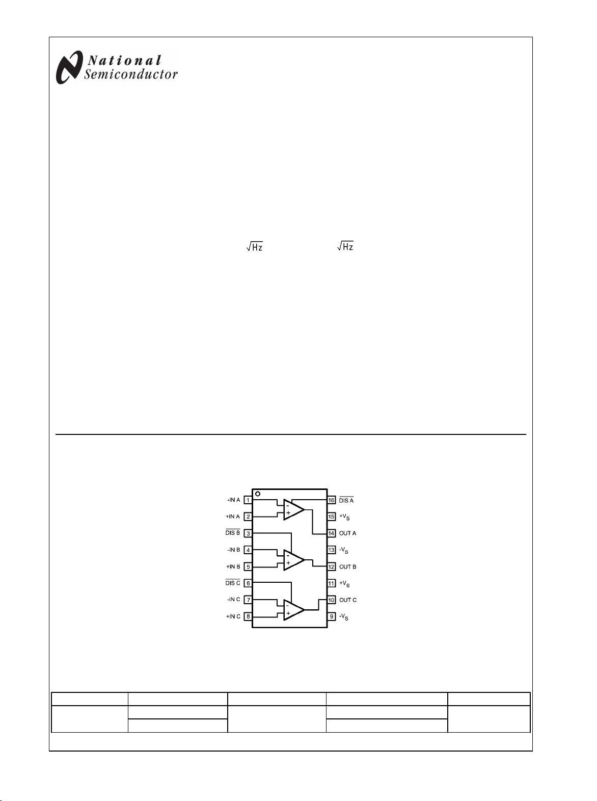
The LMH6733 is offered in a 16-Pin SSOP package with flow
through pinout for ease of layout and is also pin compatible
with the LMH6738. Each amplifier has an individual shutdown
pin.
input
Features
Supply range 3 to 12V single supply
■
Supply range ±1.5V to ±6V split supply
■
1.0 GHz −3 dB small signal bandwidth
■
(AV = +1, VS = ±5V)
650 MHz −3 dB small signal bandwidth
■
(AV = +2, VS = 5V)
Low supply current (5.5 mA per op amp, VS = 5V)
■
2.1 nV/
■
3750 V/μs slew rate
■
70 mA linear output current
■
CMIR and output swing to 1V from each supply rail
■
input noise voltage
Applications
HDTV component video driver
■
High resolution projectors
■
Flash A/D driver
■
D/A transimpedance buffer
■
Wide dynamic range IF amp
■
Radar/communication receivers
■
DDS post-amps
■
Wideband inverting summer
■
Line driver
■
Connection Diagram
16-Pin SSOP
Top View
20199110
Ordering Information
Package Part Number Package Marking Transport Media NSC Drawing
16-pin SSOP
VIP10™ is a trademark of National Semiconductor Corporation.
LMH6733MQ
LMH6733MQX 2.5k Units Tape and Reel
LH6733MQ
95 Units/Rail
MQA16
© 2007 National Semiconductor Corporation 201991 www.national.com
Absolute Maximum Ratings (Note 1)
If Military/Aerospace specified devices are required,
please contact the National Semiconductor Sales Office/
LMH6733
Distributors for availability and specifications.
ESD Tolerance (Note 2)
Human Body Model 2000V
Machine Model 200V
Supply Voltage (V+ - V–)
I
OUT
Common Mode Input Voltage ±V
Maximum Junction Temperature +150°C
13.2V
(Note 3)
CC
Soldering Information
Infrared or Convection (20 sec.) 235°C
Wave Soldering (10 sec.) 260°C
Storage Temperature Range −65°C to +150°C
Operating Ratings (Note 1)
Thermal Resistance
Package
(θJC)
16-Pin SSOP 36°C/W 120°C/W
Temperature Range (Note 4) −40°C +85°C
Supply Voltage (V+ - V–) 3V to 12V
Storage Temperature Range −65°C to +150°C
5V Electrical Characteristics (Note 5)
AV = +2, VCC = 5V, RL = 100Ω, RF = 340Ω; unless otherwise specified.
Symbol Parameter Conditions Min Typ Max Units
Frequency Domain Performance
UGBW −3 dB Bandwidth Unity Gain, V
SSBW −3 dB Bandwidth
SSBW
LSBW V
0.1 dBBW0.1 dB Gain Flatness V
V
= 200 mVPP, RL = 100Ω
OUT
V
= 200 mVPP, RL = 150Ω
OUT
= 2 V
OUT
= 200 mV
OUT
PP
= 200 mV
OUT
PP
PP
870
650
685
480
320 MHz
(θJA)
MHz
MHz
Time Domain Response
TRS Rise and Fall Time
2V Step 0.8 ns
(10% to 90%)
SR Slew Rate 2V Step 1900 V/µs
t
s
t
e
t
d
Settling Time to 0.1% 2V Step 10 ns
Enable Time From Disable = Rising Edge 10 ns
Disable Time From Disable = Falling Edge 15 ns
Distortion
HD2L 2nd Harmonic Distortion 2 VPP, 10 MHz −63 dBc
HD3L 3rd Harmonic Distortion 2 VPP, 10 MHz −73 dBc
Equivalent Input Noise
V
N
I
CN
N
CN
Non-Inverting Voltage >10 MHz 2.1
Inverting Current >10 MHz 18.6
Non-Inverting Current >10 MHz 26.9
nV/
pA/
pA/
Video Performance
DG Differential Gain
DP Differential Phase
4.43 MHz, RL = 150Ω
4.43 MHz, RL = 150Ω
0.03 %
0.025 deg
Static, DC Performance
VIO Input Offset Voltage (Note 7) 0.4 2.0
2.5
IBN Input Bias Current (Note 7) Non-Inverting 2 16.7 28
32
IBI Input Bias Current (Note 7) Inverting 1.0 17
19
PSRR Power Supply Rejection Ratio
(Note 7)
+PSRR 59
59
−PSRR 58
61
61
mV
µA
μA
dB
57
www.national.com 2
Symbol Parameter Conditions Min Typ Max Units
CMRR Common Mode Rejection Ratio
(Note 7)
XTLK Crosstalk Input Referred, f = 10 MHz, Drive
52
51.5
54.5
dB
−80 dB
Channels A,C Measure Channel B
I
CC
Supply Current Disabled V
Supply Current Disabled V
Supply Current (Note 7) All Three Amps Enabled, No Load 16.7 18 mA
+
−
RL = ∞
RL = ∞
1.54 1.8 mA
0.75 1.8 mA
Miscellaneous Performance
RIN+ Non-Inverting Input Resistance 200
kΩ
CIN+ Non-Inverting Input Capacitance 1 pF
RIN− Inverting Input Impedance Output Impedance of Input Buffer. 27
R
O
V
O
Output Impedance DC 0.05
Output Voltage Range (Note 7)
RL = 100Ω
RL = ∞
1.25-3.75
1.3-3.7
1.11-3.89
1.12-3.88
1.03-3.97
Ω
Ω
V
1.15-3.85
CMIR Common Mode Input Range
(Note 7)
I
O
Linear Output Current
CMRR > 40 dB 1.1-3.9
1.2-3.8
VIN = 0V, V
< ±42 mV ±50 ±60 mA
OUT
1.0–4.0
V
(Notes 3, 7)
I
SC
I
IH
I
IL
V
V
DMAX
DMIM
Short Circuit Current (Note 6) VIN = 2V Output Shorted to Ground 170 mA
Disable Pin Bias Current High Disable Pin = V
Disable Pin Bias Current Low Disable Pin = 0V −360
Voltage for Disable
Voltage for Enable
Disable Pin ≤ V
Disable Pin ≥ V
+
DMAX
DMIN
−72
3.2 V
3.6 V
μA
μA
LMH6733
±5V Electrical Characteristics (Note 5)
AV = +2, VCC = ±5V, RL = 100Ω, RF = 383Ω; unless otherwise specified.
Symbol Parameter Conditions Min Typ Max Units
Frequency Domain Performance
UGBW −3 dB Bandwidth Unity Gain, V
SSBW −3 dB Bandwidth
SSBW
LSBW V
0.1 dB BW 0.1 dB Gain Flatness V
V
= 200 mVPP, RL = 100Ω
OUT
V
= 200 mVPP, RL = 150Ω
OUT
= 2 V
OUT
= 200 mV
OUT
Time Domain Response
TRS Rise and Fall Time
TRL 5V Step 0.8
(10% to 90%)
2V Step 0.7
SR Slew Rate 4V Step 3750 V/µs
t
s
t
e
t
d
Settling Time to 0.1% 2V Step 10 ns
Enable Time From Disable = Rising Edge 10 ns
Disable Time From Disable = Falling Edge 15 ns
Distortion
HD2L 2nd Harmonic Distortion 2 VPP, 10 MHz −72 dBc
HD3L 3rd Harmonic Distortion 2 VPP, 10 MHz −63 dBc
Equivalent Input Noise
V
N
I
CN
Non-Inverting Voltage >10 MHz 2.1
Inverting Current >10 MHz 18.6
PP
= 200 mV
OUT
PP
PP
1000 MHz
830
950
MHz
600
350
MHz
ns
nV/
pA/
3 www.national.com
Symbol Parameter Conditions Min Typ Max Units
N
CN
LMH6733
Video Performance
DG Differential Gain
DP Differential Phase
Non-Inverting Current >10 MHz 26.9
4.43 MHz, RL = 150Ω
4.43 MHz, RL = 150Ω
0.03 %
0.03 Deg
Static, DC Performance
VIO Input Offset Voltage (Note 7) 0.6 2.2
2.5
IBN Input Bias Current (Note 7) Non-Inverting −14
−19
3.5 19
24
IBI Input Bias Current (Note 7) Inverting 5 23
26
PSRR Power Supply Rejection Ratio
(Note 7)
CMRR Common Mode Rejection Ratio
(Note 7)
XTLK Crosstalk Input Referred, f = 10 MHz, Drive
+PSRR 59 61.5
−PSRR 58 61
53
55
52.5
−80 dB
Channels A,C Measure Channel B
I
CC
Supply Current (Note 7) All Three Amps Enabled, No Load 19.5 20.8
22.0
Supply Current Disabled V
Supply Current Disabled V
+
−
RL = ∞
RL = ∞
1.54 1.8 mA
0.75 1.8 mA
Miscellaneous Performance
RIN+ Non-Inverting Input Resistance 200
CIN+ Non-Inverting Input Capacitance 1 pF
RIN− Inverting Input Impedance Output Impedance of Input Buffer 30
R
O
V
O
CMIR Common Mode Input Range
I
O
Output Impedance DC 0.05
Output Voltage Range (Note 7)
(Note 7)
Linear Output Current
RL = 100Ω
RL = ∞
CMRR > 43 dB ±3.9
VIN = 0V, V
< ±42 mV 70 ±80 mA
OUT
±3.55
±3.5
±3.7
±3.85 ±4.0
±4.0 V
±3.8
(Notes 3, 7)
I
SC
I
IH
I
IL
V
V
DMAX
DMIM
Short Circuit Current (Note 6) VIN = 2V Output Shorted to Ground 237 mA
Disable Pin Bias Current High Disable Pin = V
+
−72
Disable Pin Bias Current Low Disable Pin = 0V −360
Voltage for Disable
Voltage for Enable
Disable Pin ≤ V
Disable Pin ≥ V
DMAX
DMIN
3.2 V
3.6 V
pA/
mV
µA
μA
dB
dB
mA
kΩ
Ω
Ω
V
μA
μA
Note 1: Absolute Maximum Ratings indicate limits beyond which damage to the device may occur. Operating Ratings indicate conditions for which the device is
intended to be functional, but specific performance is not guaranteed. For guaranteed specifications, see the Electrical Characteristics tables.
Note 2: Human Body Model, applicable std. MIL-STD-883, Method 3015.7. Machine Model, applicable std. JESD22-A115-A (ESD MM std. of JEDEC)
Field-Induced Charge-Device Model, applicable std. JESD22-C101-C (ESD FICDM std. of JEDEC).
Note 3: The maximum output current (I
for more details.
Note 4: The maximum power dissipation is a function of T
PD = (T
Note 5: Electrical Table values apply only for factory testing conditions at the temperature indicated. Factory testing conditions result in very limited self-heating
of the device such that TJ = TA. No guarantee of parametric performance is indicated in the electrical tables under conditions of internal self-heating where
TJ > TA.
Note 6: Short circuit current should be limited in duration to no more than 10 seconds. See the Power Dissipation section of the Application Section for more
details.
Note 7: Parameter 100% production tested at 25° C.
www.national.com 4
– TA)/ θJA. All numbers apply for packages soldered directly onto a PC Board.
J(MAX)
) is determined by device power dissipation limitations. See the Power Dissipation section of the Applications Information
OUT
, θJA. The maximum allowable power dissipation at any ambient temperature is
J(MAX)
LMH6733
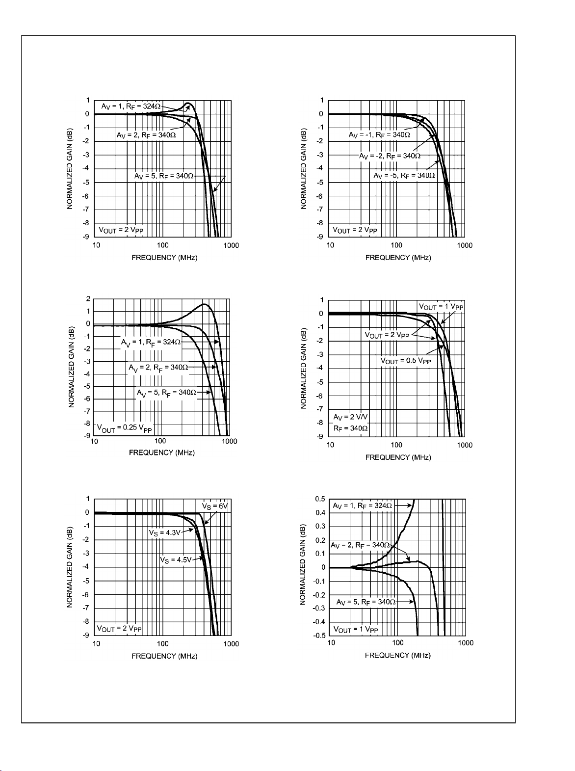
Typical Performance Characteristics A
specified).
Large Signal Frequency Response
20199111
Small Signal Frequency Response
= +2, VCC = 5V, RL = 100Ω, RF = 340Ω; unless otherwise
V
Large Signal Frequency Response
20199112
Frequency Response vs. V
OUT
20199113
Frequency Response vs. Supply Voltage
20199115
20199114
Gain Flatness
20199116
5 www.national.com
 Loading...