

查询LMH6702供应商
LMH6702
Ultra Low Distortion, Wideband Op Amp
LMH6702 Ultra Low Distortion, Wideband Op Amp
June 2003
General Description
The LMH6702 is a very wideband, DC coupled monolithic
operational amplifier designed specifically for wide dynamic
range systems requiring exceptional signal fidelity. Benefiting from National’s current feedback architecture, the
LMH6702 offers unity gain stability at exceptional speed
without need for external compensation.
With its 720MHz bandwidth (A
distortion levels through 60MHz (R
input referred noise and 12.5mA supply current, the
LMH6702 is the ideal driver or buffer for high-speed flash
A/D and D/A converters.
Wide dynamic range systems such as radar and communication receivers, requiring a wideband amplifier offering exceptional signal purity, will find the LMH6702’s low input
referred noise and low harmonic and intermodulation distortion make it an attractive high speed solution.
The LMH6702 is constructed using National’s VIP10
plimentary bipolar process and National’s proven current
feedback architecture. The LMH6702 is available in SOIC
and SOT23-5 packages.
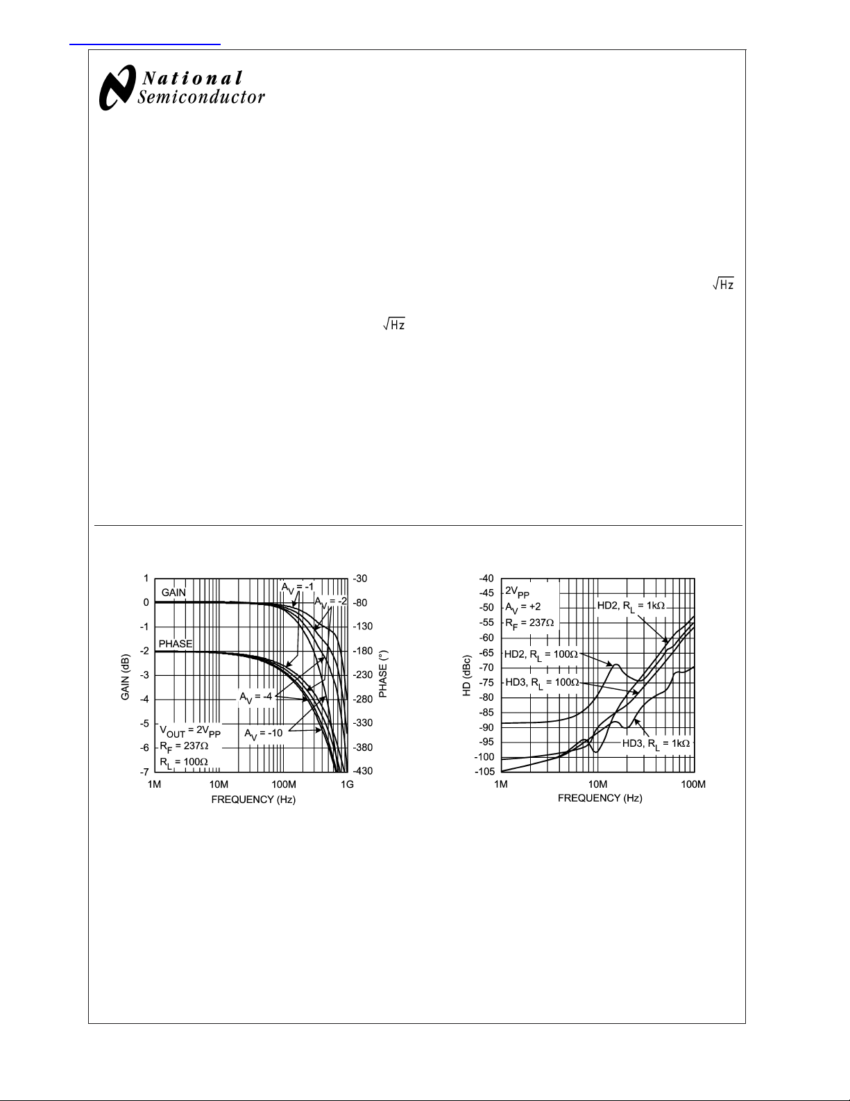
Inverting Frequency Response Harmonic Distortion vs. Load and Frequency
= 2V/V, VO=2VPP), 10-bit
V
= 100Ω), 1.83nV/
L
™
com-
Features
VS=±5V, TA= 25˚C, AV= +2V/V, RL= 100Ω,V
Typical unless Noted:
nd/3rd
n 2
n −3dB Bandwidth (V
n Low noise 1.83nV/
n Fast settling to 0.1% 13.4ns
n Fast slew rate 3100V/µs
n Supply current 12.5mA
n Output current 80mA
n Low Intermodulation Distortion (75MHz) −67dBc
n Improved Replacement for CLC409 and CLC449
Harmonics (5MHz, SOT23-5) −100/−96dBc
=2VPP) 720MHz
OUT
OUT
=2VPP,
Applications
n Flash A/D driver
n D/A transimpedance buffer
n Wide dynamic range IF amp
n Radar/communication receivers
n Line driver
n High resolution video
20039002
© 2003 National Semiconductor Corporation DS200390 www.national.com
20039007
Absolute Maximum Ratings (Note 1)
If Military/Aerospace specified devices are required,
please contact the National Semiconductor Sales Office/
LMH6702
Distributors for availability and specifications.
V
S
I
OUT
Common Mode Input Voltage V
Maximum Junction Temperature +150˚C
Storage Temperature Range −65˚C to +150˚C
Soldering Information
Infrared or Convection (20 sec.) 235˚C
Wave Soldering (10 sec.) 260˚C
±
6.75V
(Note 3)
−
to V
+
Human Body Model 2000V
Machine Model 200V
Storage Temperature Range −65˚C to +150˚C
Operating Ratings (Note 1)
Thermal Resistance
Package (θ
8-Pin SOIC 75˚C/W 160˚C/W
5-Pin SOT23 120˚C/W 187˚C/W
Operating Temperature −40˚C to +85˚C
Nominal Supply Voltage
)(θJA)
JC
±
5V to±6V
ESD Tolerance (Note 4)
Electrical Characteristics (Note 2)
AV= +2, VS=±5V, RL= 100Ω,RF= 237Ω; unless specified
Symbol Parameter Conditions Min
(Note 6)
Frequency Domain Performance
SSBW
SSBW
GF
0.1dB
-3dB Bandwidth V
LG
LG
HG
0.1dB Gain Flatness V
=2V
OUT
V
OUT
V
OUT
OUT
PP
=4V
PP
=2VPP,AV= +10 140
=2V
PP
LPD Linear Phase Deviation DC to 100MHz 0.09 deg
DG Differential Gain R
DP Differential Phase R
=150Ω, 3.58MHz/4.43MHz 0.024/0.021 %
L
= 150Ω, 3.58MHz/4.43MHz 0.004/0.007 deg
L
Time Domain Response
TRS/TRL Rise and Fall Time 2V Step 0.87/0.77 ns
6V Step 1.70/1.70 ns
OS Overshoot 2V Step 0 %
SR Slew Rate 6V
T
s
Settling Time to 0.1% 2V Step 13.4 ns
, 40% to 60% (Note 5) 3100 V/µs
PP
Distortion And Noise Response
HD2L 2
nd
Harmonic Distortion 2VPP, 5MHz (Note 9)
(SOT23-5/SOIC)
HD2 2VPP, 20MHz (Note 9)
(SOT23-5/SOIC)
HD2H 2V
, 60MHz (Note 9)
PP
(SOT23-5/SOIC)
rd
HD3L 3
Harmonic Distortion 2VPP, 5MHz (Note 9)
(SOT23-5/SOIC)
HD3 2VPP, 20MHz (Note 9)
(SOT23-5/SOIC)
HD3H 2V
, 60MHz (Note 9)
PP
(SOT23-5/SOIC)
OIM3 IMD 75MHz, PO= 10dBm/ tone −67 dBc
V
N
I
N
Input Referred Voltage Noise
Input Referred Inverting Noise
>
1MHz 1.83 nV/
>
1MHz 18.5 pA/
Current
I
NN
Input Referred Non-Inverting
>
1MHz 3.0 pA/
Noise Current
SNF Total Input Noise Floor
>
1MHz −158 dBm
INV Total Integrated Input Noise 1MHz to 150MHz 35 µV
Typ
(Note 6)
Max
(Note 6)
720
480
120 MHz
−100/ −87 dBc
−79/ −72 dBc
−63/ −64 dBc
−96/ −98 dBc
−88/ −82 dBc
−70/ −65 dBc
Units
MHzLSBW
1Hz
www.national.com 2
Electrical Characteristics (Note 2) (Continued)
AV= +2, VS=±5V, RL= 100Ω,RF= 237Ω; unless specified
Symbol Parameter Conditions Min
(Note 6)
Static, DC Performance
V
DV
IO
IO
Input Offset Voltage
Input Offset Voltage Average
(Note 8) −13 µV/˚C
Drift
I
DI
I
DI
BN
BN
BI
BI
Input Bias Current Non-Inverting (Note 7) −6
Input Bias Current Average Drift Non-Inverting (Note 8) +40 nA/˚C
Input Bias Current Inverting (Note 7) −8
Input Bias Current Average Drift Inverting (Note 8) −10 nA/˚C
PSRR Power Supply Rejection Ratio DC 47
45
CMRR Common Mode Rejection Ration DC 45
44
I
CC
Supply Current RL=
∞
11.0
10.0
Miscellaneous Performance
R
IN
C
IN
R
OUT
V
OL
CMIR Input Voltage Range Common Mode
I
O
Note 1: Absolute Maximum Ratings indicate limits beyond which damage to the device may occur. Operating Ratings indicate conditions for which the device is
intended to be functional, but specific performance is not guaranteed. For guaranteed specifications, see the Electrical Characteristics tables.
Note 2: Electrical Table values apply only for factory testing conditions at the temperature indicated. Factory testing conditions result in very limited self-heating of
the device such that T
Min/Max ratings are based on production testing unless otherwise specified.
Note 3: The maximum output current (I
Note 4: Human body model: 1.5kΩ in series with 100pF. Machine model: 0Ω in series with 200pF.
Note 5: Slew Rate is the average of the rising and falling edges.
Note 6: Typical numbers are the most likely parametric norm. Bold numbers refer to over temperature limits.
Note 7: Negative input current implies current flowing out of the device.
Note 8: Drift determined by dividing the change in parameter at temperature extremes by the total temperature change.
Note 9: Harmonic distortion is strongly influenced by package type (SOT23-5 or SOIC). See Application Note section under "Harmonic Distortion" for more
information.
Input Resistance Non-Inverting 1.4 MΩ
Input Capacitance Non-Inverting 1.6 pF
Output Resistance Closed Loop 30 mΩ
Output Voltage Range RL= 100Ω
±
3.3
±
3.2
±
1.9
Output Current 50 80 mA
. No guarantee of parametric performance is indicated in the electrical tables under conditions of internal self-heating where T
J=TA
) is determined by device power dissipation limitations.
OUT
Typ
(Note 6)
±
1.0
Max
(Note 6)
±
4.5
±
6.0
±
15
±
21
±
30
±
34
52 dB
48 dB
12.5 16.1
17.5
±
3.5 V
±
2.2 V
Units
mV
µA
µA
mA
>
J
LMH6702
TA.
www.national.com3
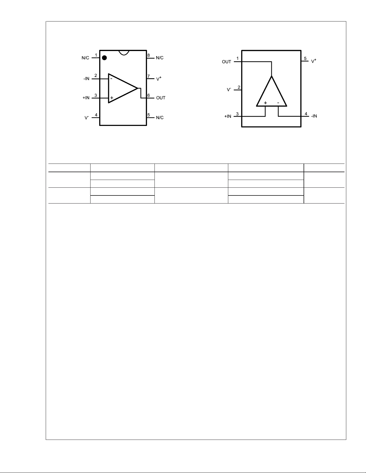
Connection Diagrams
LMH6702
8-Pin SOIC 5-Pin SOT23
Top View
20039024
Top View
Ordering Information
Package Part Number Package Marking Transport Media NSC Drawing
8-pin SOIC LMH6702MA LMH6702MA 95 Units/Rail
LMH6702MAX 2.5k Units Tape and Reel
5-Pin SOT23 LMH6702MF A83A 1k Units Tape and Reel MF05A
LMH6702MFX 3k Units Tape and Reel
20039025
M08A
www.national.com 4
 Loading...