

National Semiconductor LMH6654, LMH6655 Technical data
查询LMH6654供应商
LMH6654/55
Single/Dual Low Power, 250 MHz, Low Noise Amplifiers
LMH6654/55 Single/Dual Low Power, 250 MHz, Low Noise Amplifiers
August 2001
General Description
The LMH6654/55 single and dual high speed, voltage feedback amplifiers are designed to have unity-gain stable operation with a bandwidth of 250MHz. They operate from
±
2.5V to±6V and each channel consumes only 4.5mA. The
amplifiers feature very low voltage noise and wide output
swing to maximize signal-to-noise ratio.
The LMH6654/55 have a true single supply capability with
input common mode voltage range extending 150 mV below
negative rail and within 1.3V of the positive rail.
LMH6654/55 high speed and low power combination make
these products an ideal choice for many portable, high
speed application where power is at a premium.
The LMH6654 is packaged in SOT23-5 and SOIC-8. The
LMH6655 is packaged in MSOP-8 and SOIC-8.
The LMH6654/55 are built on National’s Advance VIP10
(Vertically Integrated PNP) complementary bipolar process.
™
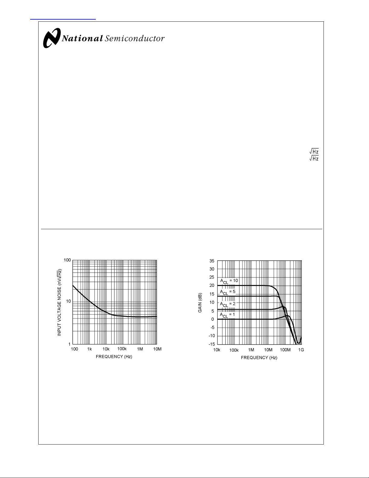
Typical Performance Characteristics
Input Voltage Noise vs. Frequency Closed Loop Gain vs. Frequency
Features
(VS=±5V, TJ= 25˚C, Typical values unless specified).
n Voltage feedback architecture
n Unity gain bandwidth 250MHz
n Supply voltage range
n Slew rate 200V/µsec
n Supply current 4.5mA/channel
n Input common mode voltage −5.15V to +3.7V
n Output voltage swing (R
n Input voltage noise 4.5nV/
n Input current noise 1.7pA/
n Settling Time to 0.01% 25ns
= 100Ω) −3.6V to 3.4V
L
±
2.5V to±6V
Applications
n ADC drivers
n Consumer video
n Active filters
n Pulse delay circuits
n xDSL receiver
n Pre-amps
20016560 20016558
© 2001 National Semiconductor Corporation DS200165 www.national.com
Absolute Maximum Ratings (Note 1)
If Military/Aerospace specified devices are required,
please contact the National Semiconductor Sales Office/
Distributors for availability and specifications.
LMH6654/55
ESD Tolerance (Note 2)
Human Body Model 2kV
Machine Model 200V
V
Differential
IN
Output Short Circuit Duration (Note 3)
Supply Voltage (V
Voltage at Input pins V
Storage Temperature Range −65˚C to +150˚C
+−V−
) 13.2V
+
+0.5V, V−−0.5V
±
1.2V
Soldering Information
Infrared or Convection (20 sec.) 235˚C
Wave Soldering (10 sec.) 260˚C
Operating Ratings (Note 1)
Supply Voltage (V
+-V−
)
Junction Temperature Range −40˚C to +85˚C
Thermal Resistance (θ
)
JA
8-Pin SOIC 172˚C/W
8-Pin MSOP 235˚C/W
5-Pin SOT-23 265˚C/W
±
2.5V to±6.0V
Junction Temperature (Note 4) +150˚C
±
5V Electrical Characteristics
Unless otherwise specified, all limits guaranteed for TJ= 25˚C, V+= +5V, V−= −5V, VCM= 0V, AV= +1, RF=25Ωfor gain =
+1, R
= 402Ω for gain = ≥ +2, and RL= 100Ω. Boldface limits apply at the temperature extremes.
F
Symbol Parameter Conditions Min
(Note 6)
Typ
(Note 5)
Max
(Note 6)
Dynamic Performance
f
CL
GBWP Gain Bandwidth Product A
Close Loop Bandwidth AV= +1 250
A
= +2 130
V
A
=+5 52
V
A
= +10 26
V
≥ +5 260 MHz
V
Bandwidth for 0.1dB Flatness A
+1 18 MHz
V
φm Phase Margin 50 deg
SR Slew Rate (Note 8) A
T
S
Settling Time
= +1, VIN=2V
V
PP
200 V/µs
AV= +1, 2V Step 25 ns
0.01%
0.1% 15 ns
t
r
t
f
Rise Time AV= +1, 0.2V Step 1.4 ns
Fall Time AV= +1, 0.2V Step 1.2 ns
Distortion and Noise Response
e
n
i
n
Input Referred Voltage Noise f ≥ 0.1 MHz 4.5 nV/
Input-Referred Current Noise f ≥ 0.1 MHz 1.7 pA/
Second Harmonic Distortion AV= +1, f = 5MHz −80
Third Harmonic Distortion V
X
t
Crosstalk (for LMH6655 only) Input Referred, 5MHz,
=2VPP,RL= 100Ω −85
O
−80 dB
Channel-to-Channel
DG Differential Gain A
DP Differential Phase A
= +2, NTSC, RL= 150Ω 0.01 %
V
= +2, NTSC, RL= 150Ω 0.025 deg
V
Input Characteristics
V
OS
TC V
I
B
Input Offset Voltage VCM=0V −3
−4
Input Offset Average Drift VCM= 0V (Note 7) 6 µV/˚C
OS
Input Bias Current VCM=0V 5 12
±
13
4
18
I
OS
R
IN
Input Offset Current VCM=0V −1
−2
0.3 1
2
Input Resistance Common- Mode 4 MΩ
Differential Mode 20 kΩ
Units
MHz
dBc
mV
µA
µA
www.national.com 2
±
5V Electrical Characteristics (Continued)
Unless otherwise specified, all limits guaranteed for TJ= 25˚C, V+= +5V, V−= −5V, VCM= 0V, AV= +1, RF=25Ωfor gain =
+1, R
= 402Ω for gain = ≥ +2, and RL= 100Ω. Boldface limits apply at the temperature extremes.
F
Symbol Parameter Conditions Min
(Note 6)
C
IN
Input Capacitance Common- Mode 1.8 pF
Typ
(Note 5)
Max
(Note 6)
Units
Differential Mode 1
CMRR Common Mode Rejection Ration Input Referred,
V
=0Vto−5V
CM
70
68
90 dB
CMVR Input Common- Mode Voltage Range CMRR ≥ 50dB −5.15 −5.0
3.5 3.7
Transfer Characteristics
A
VOL
Large Signal Voltage Gain VO=4VPP,RL= 100Ω 60
67 dB
58
Output Characteristics
V
O
Output Swing High No Load 3.4
3.6
3.2
Output Swing Low No Load −3.9 −3.7
−3.5
Output Swing High R
= 100Ω 3.2
L
3.4
3.0
Output Swing Low R
= 100Ω −3.6 −3.4
L
−3.2
I
I
R
SC
OUT
Short Circuit Current (Note 3) Sourcing, VO=0V
= 200mV
∆V
IN
Sinking, V
∆V
IN
=0V
O
= 200mV
145
130
100
80
Output Current Sourcing, VO= +3V 80
Sinking, V
O
Output Resistance AV= +1, f<100kHz 0.08 Ω
= −3V 120
O
280
185
Power Supply
PSRR Power Supply Rejection Ratio Input Referred ,
V
=±5V to±6V
S
I
S
Supply Current (per channel) 4.5 6
60 76 dB
7
LMH6654/55
V
V
mA
mA
mA
5V Electrical Characteristics
Unless otherwise specified, all limits guaranteed for TJ= 25˚C, V+= +5V, V−= −0V, VCM= 2.5V, AV= +1, RF=25Ωfor gain
= +1, R
Symbol Parameter Conditions Min
Dynamic Performance
f
CL
GBWP Gain Bandwidth Product A
φm Phase Margin 48 deg
SR Slew Rate (Note 8) A
T
S
= 402Ω for gain = ≥ +2, and RL= 100Ω to V+/2. Boldface limits apply at the temperature extremes.
F
(Note 6)
Typ
(Note 5)
Max
(Note 6)
Close Loop Bandwidth AV= +1 230
A
= +2 120
V
A
=+5 50
V
A
= +10 25
V
≥ +5 250 MHz
V
Bandwidth for 0.1dB Flatness A
Settling Time
= +1 17 MHz
V
= +1, VIN=2V
V
PP
190 V/µs
AV= +1, 2V Step 30 ns
0.01%
0.1% 20 ns
Units
MHz
www.national.com3
5V Electrical Characteristics (Continued)
Unless otherwise specified, all limits guaranteed for TJ= 25˚C, V+= +5V, V−= −0V, VCM= 2.5V, AV= +1, RF=25Ωfor gain
= +1, R
LMH6654/55
Symbol Parameter Conditions Min
t
r
t
f
Distortion and Noise Response
e
n
i
n
X
t
Input Characteristics
V
OS
TC V
I
B
I
OS
R
IN
C
IN
CMRR Common Mode Rejection Ration Input Referred,
CMVR Input Common Mode Voltage Range CMRR ≥ 50dB −0.15 0
Transfer Characteristics
A
VOL
Output Characteristics
V
O
I
SC
I
OUT
R
O
Power Supply
PSRR Power Supply Rejection Ratio Input Referred ,
I
S
= 402Ω for gain = ≥ +2, and RL= 100Ω to V+/2. Boldface limits apply at the temperature extremes.
F
(Note 6)
Typ
(Note 5)
Max
(Note 6)
Rise Time AV= +1, 0.2V Step 1.5 ns
Fall Time AV= +1, 0.2V Step 1.35 ns
Input Referred Voltage Noise f ≥ 0.1MHz 4.5 nV/
Input Referred Current Noise f ≥ 0.1 MHz 1.7 pA/
Second Harmonic Distortion AV= +1, f = 5MHz −65
Third Harmonic Distortion V
=2VPP,RL= 100Ω −70
O
Crosstalk (for LMH6655 only) Input Referred, 5MHz −78 dB
Input Offset Voltage VCM= 2.5V −5
−6.5
Input Offset Average Drift VCM= 2.5V (Note 7) 6 µV/˚C
OS
±
25
6.5
Input Bias Current VCM= 2.5V 6 12
18
Input Offset Current VCM= 2.5V −2
0.5 2
−3
Input Resistance Common- Mode 4 MΩ
Differential Mode 20 kΩ
Input Capacitance Common- Mode 1.8 pF
Differential Mode 1
V
= 0V to −2.5V
CM
70
68
90 dB
3.5 3.7
Large Signal Voltage Gain VO= 1.6VPP,RL= 100Ω 58
64 dB
55
Output Swing High No Load 3.6
3.75
3.4
Output Swing Low No Load 0.9 1.1
1.3
Output Swing High R
= 100Ω 3.5
L
3.70
3.35
Output Swing Low R
= 100Ω 1 1.3
L
1.45
Short Circuit Current (Note 3) Sourcing , VO= 2.5V
= 200mV
∆V
IN
Sinking, V
∆V
IN
= 2.5V
O
= 200mV
90
80
70
60
170
140
Output Current Sourcing, VO= +3.5V 30
Sinking, V
= 1.5V 60
O
Output Resistance AV= +1, f<100kHz .08 Ω
60 75 dB
V
=±2.5V to±3V
S
Supply Current (per channel) 4.5 6
3
7
Units
dBc
mV
µA
µA
V
V
mA
mA
mA
www.national.com 4
5V Electrical Characteristics (Continued)
Note 1: Absolute Maximum Ratings indicate limits beyond which damage to the device may occur. Operating Ratings indicate conditions for which the device is
intended to be functional, but specificperformanceisnotguaranteed.For guaranteed specifications and the test conditions, see the Electrical Characteristics Table.
Note 2: Human body model, 1.5kΩ in series with 100pF. Machine model: 0Ω in series with 100pF.
Note 3: Continuous short circuit operation at elevated ambient temperature can result in exceeding the maximum allowed junction temperature at 150˚C.
Note 4: The maximum power dissipation is a function of T
(T
J(MAX)−TA
Note 5: Typical Values represent the most likely parametric norm.
Note 6: All limits are guaranteed by testing or statistical analysis.
Note 7: Offset voltage average drift is determined by dividing the change in V
Note 8: Slew rate is the slower of the rising and falling slew rates. Slew rate is rate of change from 10% to 90% of output voltage step.
)/θJA. All numbers apply for packages soldered directly onto a PC board.
, θJAand TA. The maximum allowable power dissipation at any ambient temperature is PD=
J(MAX)
at temperature extremes into the total temperature change.
OS
LMH6654/55
Typical Performance Characteristics T
402Ω and for gain ≥ +2, and R
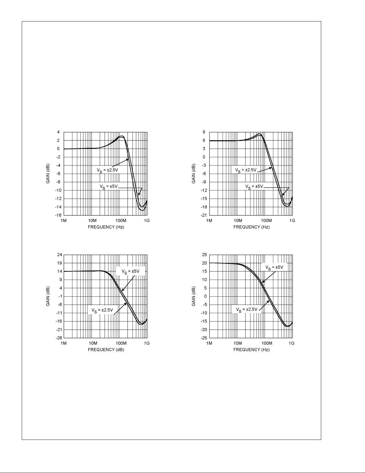
Closed Loop Bandwidth (G = +1) Closed Loop Bandwidth (G = +2)
Closed Loop Bandwidth (G = +5) Closed Loop Bandwidth (G = +10)
= 100Ω, unless otherwise specified.
L
20016509 20016510
= 25˚C, V+=±5V, V−= −5, RF=25Ωfor gain = +1, RF=
J
20016511 20016512
www.national.com5
Typical Performance Characteristics T
402Ω and for gain ≥ +2, and R
= 100Ω, unless otherwise specified. (Continued)
L
= 25˚C, V+=±5V, V−= −5, RF=25Ωfor gain = +1, RF=
J
LMH6654/55
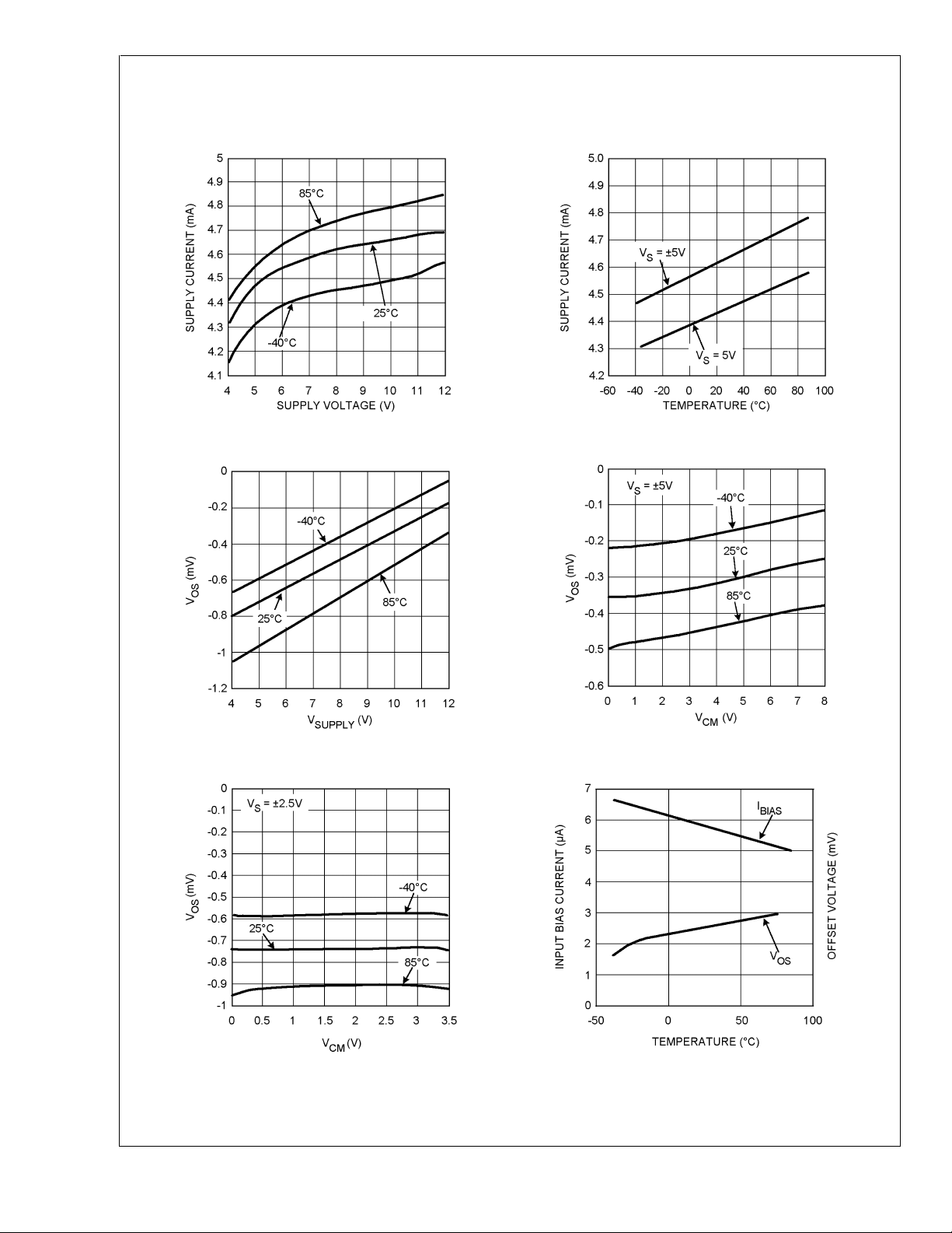
Supply Current per Channel vs. Supply Voltage Supply Current per Channel vs. Temperature
Offset Voltage vs. Supply Voltage (VCM= 0V) Offset Voltage vs. Common Mode
20016535 20016548
20016549
Offset Voltage vs. Common Mode Bias Current and Offset Voltage vs. Temperature
20016539
www.national.com 6
20016532
20016551
 Loading...