

查询LMH6609供应商
LMH6609
900MHz Voltage Feedback Op Amp
LMH6609 900MHz Voltage Feedback Op Amp
August 2003
General Description
The LMH6609 is an ultra wideband, unity gain stable, low
power, voltage feedback op amp that offers 900MHz bandwidth at a gain of 1, 1400V/µs slew rate and 90mA of linear
output current.
The LMH6609 is designed with voltage feedback architecture for maximum flexibility especially for active filters and
integrators. The LMH6609 has balanced, symmetrical inputs
with well-matched bias currents and minimal offset voltage.
With Differential Gain of .01 and Differential Phase of .026
the LMH6609 is suited for video applications. The 90mA of
linear output current makes the LMH6609 suitable for multiple video loads and cable driving applications as well.
The recommended supply voltage range of 6V to 12V and is
specified at 6.6 and 10V. A low supply current of 7mA (at 10V
supply) makes the LMH6609 useful in a wide variety of
platforms, including portable or remote equipment that must
run from battery power.
The LMH6609 is available in the industry standard 8-pin
SOIC package and in the space-saving 5-pin SOT package.
The LMH6609 is specified for operation over the -40˚C to
+85˚C temperature range. The LMH6609 is manufactured in
National Semiconductor’s state-of-the-art VIP10
ogy for high performance.
™
technol-
Typical Application
Features
n 900MHz −3dB bandwidth (AV=1)
n Large signal bandwidth and slew rate 100% tested
n 280MHz −3dB bandwidth (A
n 90mA linear output current
n 1400V/µs slew rate
n Unity gain stable
<
n
1mV input Offset voltage
n 7mA Supply current (no load)
n 6V to 12V supply voltage range
n .01/ .026 differential gain/phase PAL
n 3.1nV/
n Improved replacement for CLC440, 420, 426
voltage noise
= +2, V
V
OUT
=2VPP)
Applications
n Test equipment
n IF/RF amplifier
n A/D Input driver
n Active filter
n Integrator
n DAC output buffer
n Transimpedance amplifier
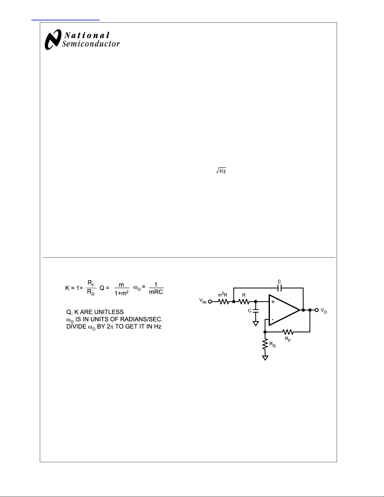
20079037
Sallen Key Low Pass Filter
© 2003 National Semiconductor Corporation DS200790 www.national.com
20079038
Absolute Maximum Ratings (Note 1)
Machine Model 200V
If Military/Aerospace specified devices are required,
please contact the National Semiconductor Sales Office/
LMH6609
Distributors for availability and specifications.
(V+-V−)
V
S
I
OUT
Common Mode Input Voltage V+ to V−
Maximum Junction Temperature +150˚C
Storage Temperature Range −65˚C to +150˚C
Lead Temperature Range +300˚C
ESD Tolerance (Note 4)
±
6.6V
(Note 3)
Operating Ratings (Note 3)
Thermal Resistance
Package (θ
8-Pin SOIC 65˚C/W 145˚C/W
5-Pin SOT23 120˚C/W 187˚C/W
Operating Temperature −40˚C +85˚C
Nominal Supply Voltage
(Note 6)
)(θJA)
JC
±
3.3V
Human Body Model 2000V
±
5V Electrical Characteristics
Unless specified, AV= +2, RF= 250Ω:VS=±5V, RL= 100Ω; unless otherwise specified. Boldface limits apply over temperature Range. (Note 2)
Symbol Parameter Conditions Min Typ Max Units
Frequency Domain Response
SSBW −3dB Bandwidth V
LSBW −3dB Bandwidth V
SSBWG1 −3dB Bandwidth A
=1 V
V
OUT
OUT
OUT
= 0.5V
= 4.0V
= 0.25V
PP
PP
PP
150 170 MHz
260 MHz
900 MHz
GFP .1dB Bandwidth Gain is Flat to .1dB 130 MHz
DG Differential Gain R
DP Differential Phase R
= 150Ω, 4.43MHz 0.01 %
L
= 150Ω, 4.43MHz 0.026 deg
L
Time Domain Response
TRS Rise and Fall Time 1V Step 1.6 ns
TRL 4V Step 2.6 ns
t
s
Settling Time to 0.05% 2V Step 15 ns
SR Slew Rate 4V Step (Note 5) 1200 1400 V/µs
Distortion and Noise Response
HD2 2
HD3 3
nd
Harmonic Distortion 2VPP, 20MHz −63 dBc
rd
Harmonic Distortion 2VPP, 20MHz −57 dBc
Equivalent Input Noise
VN Voltage Noise
CN Current Noise
>
1MHz 3.1 nV/
>
1MHz 1.6 pA/
Static, DC Performance
V
IO
I
BN
I
BI
Input Offset Voltage
Input Bias Current −2
Input Offset Current .1
PSRR Power Supply Rejection Ratio DC, 1V Step 67
±
0.8
73 dB
±
2.5
±
3.5
±
5
±
8
±
1.5
±
3
65
CMRR Common Mode Rejection Ratio DC, 2V Step 67
73 dB
65
I
CC
Supply Current RL=
∞
7.0 7.8
8.5
Miscellaneous Performance
R
IN
C
IN
R
OUT
Input Resistance 1MΩ
Input Capacitance 1.2 pF
Output Resistance Closed Loop 0.3 Ω
±
6V
mV
µA
µA
mA
www.national.com 2
±
5V Electrical Characteristics (Continued)
Unless specified, AV= +2, RF= 250Ω:VS=±5V, RL= 100Ω; unless otherwise specified. Boldface limits apply over temperature Range. (Note 2)
Symbol Parameter Conditions Min Typ Max Units
V
O
V
OL
Output Voltage Range RL=
∞
RL= 100Ω
CMIR Input Voltage Range Common Mode, CMRR>60dB
I
O
±
Linear Output Current V
3.3V Electrical Characteristics
OUT
±
3.6
±
3.3
±
3.2
±
3.0
±
2.8
±
2.5
±
60
±
50
±
3.9 V
±
3.5 V
±
3.0 V
±
90 mA
Unless specified, AV= +2, RF= 250Ω:VS=±3.3V, RL= 100Ω; unless otherwise specified. Boldface limits apply over temperature Range. (Note 2)
Symbol Parameter Conditions Min Typ Max Units
Frequency Domain Response
SSBW −3dB Bandwidth V
LSBW −3dB Bandwidth V
SSBWG1 −3dB Bandwidth A
=1 V
V
GFP .1dB Bandwidth V
DG Differential Gain R
DP Differential Phase R
= 0.5V
OUT
OUT
OUT
OUT
= 150Ω, 4.43MHz .01 %
L
= 150Ω, 4.43MHz .06 deg
L
= 3.0V
= 0.25V
=1V
PP
PP
PP
PP
180 MHz
110 MHz
450 MHz
40 MHz
Time Domain Response
TRL 1V Step 2.2 ns
SR Slew Rate 2V Step (Note 5) 800 V/µs
Distortion and Noise Response
HD2 2
HD3 3
nd
Harmonic Distortion 2VPP, 20MHz −63 dBc
rd
Harmonic Distortion 2VPP, 20MHz −43 dBc
Equivalent Input Noise
VN Voltage Noise
CN Current Noise
>
1MHz 3.7 nV/
>
1MHz 1.1 pA/
Static, DC Performance
V
IO
I
BN
I
BI
Input Offset Voltage 0.8
Input Bias Current −1
Input Offset Current 0
±
2.5
±
3.5
±
3
±
6
±
1.5
±
3
mV
µA
µA
PSRR Power Supply Rejection Ratio DC, .5V Step 67 73 dB
CMRR Common Mode Rejection Ratio DC, 1V Step 67 75 dB
I
CC
Supply Current RL=
∞
3.6 5
mA
6
Miscellaneous Performance
R
OUT
V
O
V
OL
CMIR Input Voltage Range Common Mode
I
O
Input Resistance Close Loop .05 Ω
Output Voltage Range RL=
RL= 100Ω
Linear Output Current V
OUT
∞
±
2.1
±
1.9
±
30
±
2.3 V
±
2.0 V
±
1.3 V
±
45 mA
LMH6609
www.national.com3
±
3.3V Electrical Characteristics (Continued)
Note 1: Absolute Maximum Ratings indicate limits beyond which damage to the device may occur. Operating Ratings indicate conditions for which the device is
intended to be functional, but specific performance is not guaranteed. For guaranteed specifications, see the Electrical Characteristics tables.
LMH6609
Note 2: Electrical Table values apply only for factory testing conditions at the temperature indicated. Factory testing conditions result in very limited self-heating of
the device such that T
See Applications Section for information on temperature derating of this device. Min/Max ratings are based on product characterization and simulation. Individual
parameters are tested as noted.
Note 3: The maximum output current (I
more details.
Note 4: Human body model, 1.5kΩ in series with 100pF. Machine model, 0Ω In series with 200pF.
Note 5: rate is Average of Rising and Falling 40-60% slew rates.
Note 6: Nominal Supply voltage range is for supplies with regulation of 10% or better.
. No guarantee of parametric performance is indicated in the electrical tables under conditions of internal self heating where T
J=TA
) is determined by device power dissipation limitations. See the Power Dissipation section of the Application Section for
OUT
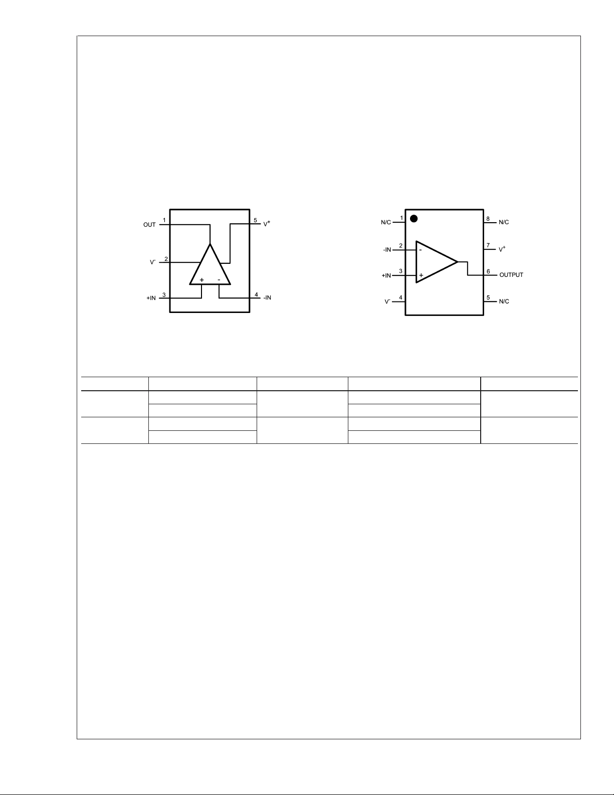
Connection Diagrams
5-Pin SOT23 8-Pin SOIC
>
TA.
J
Top View
20079039
Top View
20079040
Ordering Information
Package Part Number Package Marking Transport Media NSC Drawing
8-Pin SOIC
5-SOT23
LMH6609MA
LMH6609MAX 2.5k Units Tape and Reel
LMH6609MF
LMH6609MFX 2.5k Units Tape and Reel
LMH6609MA
A89A
95 Units/Rails
1k Units Tape and Reel
M08A
MF05A
www.national.com 4
Typical Performance Characteristics
Small Signal Non-Inverting Frequency Response Large Signal Non-Inverting Frequency Response
20079004 20079003
Small Signal Inverting Frequency Response Large Signal Inverting Frequency Response
LMH6609
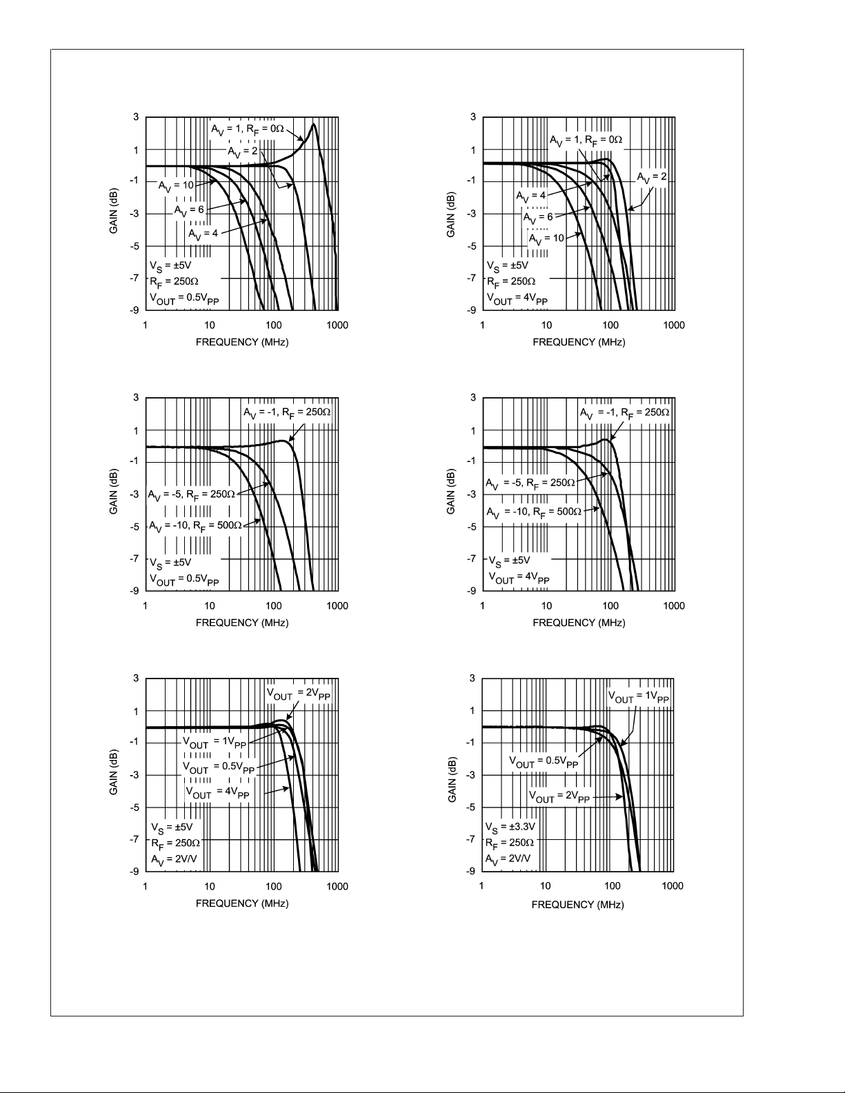
Frequency Response vs. V
OUTAV
20079002 20079010
= 2 Frequency Response vs. V
20079009
OUTAV
=2
20079001
www.national.com5

Typical Performance Characteristics (Continued)
LMH6609
Frequency Response vs. V
Frequency Response vs. V
OUTAV
OUTAV
= 1 Frequency Response vs. V
20079007 20079008
OUTAV
=−1
= −1 Frequency Response vs. Cap Load
20079006
Frequency Response vs. Cap Load Suggested R
20079043
www.national.com 6
vs. Cap Load
OUT
20079042
20079041

Typical Performance Characteristics (Continued)
CMRR vs. Frequency PSRR vs. Frequency
LMH6609
20079011
PSRR vs. Frequency Pulse Response
20079013 20079016
Pulse Response Large Signal Pulse Response
20079012
20079014
20079015
www.national.com7

Typical Performance Characteristics (Continued)
LMH6609
Noise vs. Frequency HD2 vs. V
20079025
HD3 vs. V
OUT
HD2 vs. V
OUT
20079018
OUT
20079017
HD3 vs. V
OUT
20079019
www.national.com 8
20079020
HD2 & HD3 vs. Frequency
20079021

Typical Performance Characteristics (Continued)
HD2 & HD3 vs. Frequency Differential Gain & Phase
LMH6609
20079022
Differential Gain & Phase Open Loop Gain & Phase
20079047
Open Loop Gain & Phase Closed Loop Output Resistance
20079046
20079044
20079045
20079023
www.national.com9

Application Section
GENERAL DESIGN EQUATION
LMH6609
The LMH6609 is a unity gain stable voltage feedback amplifier. The matched input bias currents track well over temperature. This allows the DC offset to be minimized by
matching the impedance seen by both inputs.
GAIN
The non-inverting and inverting gain equations for the
LMH6609 are as follows:
20079028
FIGURE 2. Typical Inverting Application
20079027
FIGURE 1. Typical Non-Inverting Application
www.national.com 10
20079029
FIGURE 3. Single Supply Inverting

Application Section (Continued)
20079030
FIGURE 4. AC Coupled Non-Inverting
GAIN BANDWIDTH PRODUCT
The LMH6609 is a voltage feedback amplifier, whose
closed-loop bandwidth is approximately equal to the gainbandwidth product (GBP) divided by the gain (A
greater than 5, A
sets the closed-loop bandwidth of the
V
LMH6609.
). For gains
V
time. Refer to the Driving Capacitive Loads section for guidance on selecting an output resistor for driving capacitive
loads.
EVALUATION BOARDS
National Semiconductor provides the following evaluation
boards as a guide for high frequency layout and as an aid in
device testing and characterization. Many of the datasheet
plots were measured with these boards.
Device Package Board Part
#
LMH6609MA SOIC CLC730227
LMH6609MF SOT-23 CLC730216
A free evaluation board is automatically shipped when a
sample request is placed with National Semiconductor.
CIRCUIT LAYOUT CONSIDERATION
A proper printed circuit layout is essential for achieving high
frequency performance. National provides evaluation boards
for the LMH6609 as shown above. These boards were laid
out for optimum, high-speed performance. The ground plane
was removed near the input and output pins to reduce
parasitic capacitance. Also, all trace lengths were minimized
to reduce series inductances.
Supply bypassing is required for the amplifiers performance.
The bypass capacitors provide a low impedance return current path at the supply pins. They also provide high frequency filtering on the power supply traces. 10µF tantalum
and .01µF capacitors are recommended on both supplies
(from supply to ground). In addition a .1µF ceramic capacitor
can be added from V
+
to V−to aid in second harmonic
suppression.
LMH6609
20079031
For Gains less than 5, refer to the frequency response plots
to determine maximum bandwidth. For large signal bandwidth the slew rate is a more accurate predictor of bandwidth.
20079032
Where f
= bandwidth, SR= Slew rate and VP= peak
MAX
amplitude.
OUTPUT DRIVE AND SETTLING TIME PERFORMANCE
The LMH6609 has large output current capability. The
100mA of output current makes the LMH6609 an excellent
choice for applications such as:
Video Line Drivers
•
Distribution Amplifiers
•
When driving a capacitive load or coaxial cable, include a
series resistance R
to back match or improve settling
OUT
20079033
FIGURE 5. Driving Capacitive Loads with R
OUT
for
Improved Stability
DRIVING CAPACITIVE LOADS
Capacitive output loading applications will benefit from the
use of a series output resistor R
of a series output resistor, R
. Figure 5 shows the use
OUT
as it might be applied when
OUT
driving an analog to digital converter. The charts "Suggested
vs. Cap Load" in the Typical Performance Section give a
R
O
recommended value for mitigating capacitive loads. The values suggested in the charts are selected for .5dB or less of
peaking in the frequency response. This gives a good compromise between settling time and bandwidth. For applications where maximum frequency response is needed and
some peaking is tolerable, the value of R
can be reduced
O
slightly from the recommended values. There will be amplitude lost in the series resistor unless the gain is adjusted to
compensate; this effect is most noticeable with heavy resistive loads.
www.national.com11

Application Section (Continued)
COMPONENT SELECTION AND FEEDBACK RESISTOR
LMH6609
Surface mount components are highly recommended for the
LMH6609. Leaded components will introduce unpredictable
parasitic loading that will interfere with proper device operation. Do not use wire wound resistors.
The LMH6609 operates best with a feedback resistor of
approximately 250Ω for all gains of +2 and greater and for −1
and less. With lower gains in particular, large value feedback
resistors will exaggerate the effects of parasitic capacitances
and may lead to ringing on the pulse response and frequency response peaking. Large value resistors also add
undesirable thermal noise. Feedback resistors that are much
below 100Ω will load the output stage, which will reduce
voltage output swing, increase device power dissipation,
increase distortion and reduce current available for driving
the load.
In the buffer configuration the output should be shorted
directly to the inverting input. This feedback does not load
the output stage because the inverting input is a high impedance point and there is no gain set resistor to ground.
OPTIMIZING DC ACCURACY
The LMH6609 offers excellent DC accuracy. The wellmatched inputs of this amplifier allows even better performance if care is taken to balance the impedances seen by
the two inputs. The parallel combination of the gain setting
and feedback RFresistors should be equal to R
R
G
resistance of the source driving the op amp in parallel with
any terminating Resistor (See Figure 1). Combining this with
the non inverting gain equation gives the following parameters:
R
F=AVRSEQ
RG=RF/(AV−1)
For Inverting gains the bias current cancellation is accom-
plished by placing a resistor R
equal in value to the resistance seen by the inverting input
(See Figure 2). R
B=RF
|| (RG+RS)
The additional noise contribution of R
the use of a shunt capacitor (not shown).
POWER DISSIPATION
The LMH6609 has the ability to drive large currents into low
impedance loads. Some combinations of ambient temperature and device loading could result in device overheating.
For most conditions peak power values are not as important
as RMS powers. To determine the maximum allowable
power dissipation for the LMH6609 use the following formula:
= (150o-T
P
MAX
Where T
= Ambient temperature (˚C) and θJA = Thermal
AMB
resistance, from junction to ambient, for a given package
(˚C/W). For the SOIC package θJA is 148˚C/W, for the SOT
it is 250˚C/W. 150
o
C is the absolute maximum limit for the
internal temperature of the device.
Either forced air cooling or a heat sink can greatly increase
the power handling capability for the LMH6609.
on the non-inverting input
B
can be minimized by
B
)/θ
AMB
JA
SEQ
, the
quency content of the signal. Performance degrades as the
loading is increased, therefore best performance will be
obtained with back-terminated loads. The back termination
reduces reflections from the transmission line and effectively
masks transmission line and other parasitic capacitances
from the amplifier output stage. This means that the device
should be configured for a gain of 2 in order to have a net
gain of 1 after the terminating resistor. (See Figure 6)
20079034
FIGURE 6. Typical Video Application
ESD PROTECTION
The LMH6609 is protected against electrostatic discharge
(ESD) on all pins. The LMH6609 will survive 2000V Human
Body model or 200V Machine model events.
Under closed loop operation the ESD diodes have no effect
on circuit performance. There are occasions, however, when
the ESD diodes may be evident. For instance, if the amplifier
is powered down and a large input signal is applied the ESD
diodes will conduct.
TRANSIMPEDANCE AMPLIFIER
The low input current noise and unity gain stability of the
LMH6609 make it an excellent choice for transimpedance
applications. Figure 7 illustrates a low noise transimpedance
amplifier that is commonly implemented with photo diodes.
sets the transimpedance gain. The photo diode current
R
F
multiplied by R
determines the output voltage.
F
VIDEO PERFORMANCE
The LMH6609 has been designed to provide good performance with both PAL and NTSC composite video signals.
The LMH6609 is specified for PAL signals. NTSC performance is typically marginally better due to the lower fre-
www.national.com 12

Application Section (Continued)
20079035
Rectifier
The large bandwidth of the LMH6609 allows for high-speed
rectification. A common rectifier topology is shown in Figure
and R2set the gain of the rectifier.
8.R
1
LMH6609
FIGURE 7. Transimpedance Amplifier
The capacitances are defined as:
CD= Equivalent Diode Capacitance
•
CF= Feedback Capacitance
•
The feedback capacitor is used to give optimum flatness and
stability. As a starting point the feedback capacitance should
be chosen as
1
⁄2of the Diode capacitance. Lower feedback
capacitors will peak frequency response.
20079036
FIGURE 8. Rectifier Topology
www.national.com13

Physical Dimensions inches (millimeters)
unless otherwise noted
LMH6609
8-Pin SOIC
NS Product Number M08A
5-Pin SOT23
NS Product Number MF05A
www.national.com 14

Notes
LMH6609 900MHz Voltage Feedback Op Amp
LIFE SUPPORT POLICY
NATIONAL’S PRODUCTS ARE NOT AUTHORIZED FOR USE AS CRITICAL COMPONENTS IN LIFE SUPPORT
DEVICES OR SYSTEMS WITHOUT THE EXPRESS WRITTEN APPROVAL OF THE PRESIDENT AND GENERAL
COUNSEL OF NATIONAL SEMICONDUCTOR CORPORATION. As used herein:
1. Life support devices or systems are devices or
systems which, (a) are intended for surgical implant
into the body, or (b) support or sustain life, and
whose failure to perform when properly used in
accordance with instructions for use provided in the
2. A critical component is any component of a life
support device or system whose failure to perform
can be reasonably expected to cause the failure of
the life support device or system, or to affect its
safety or effectiveness.
labeling, can be reasonably expected to result in a
significant injury to the user.
National Semiconductor
Americas Customer
Support Center
Email: new.feedback@nsc.com
Tel: 1-800-272-9959
www.national.com
National does not assume any responsibility for use of any circuitry described, no circuit patent licenses are implied and National reserves the right at any time without notice to change said circuitry and specifications.
National Semiconductor
Europe Customer Support Center
Fax: +49 (0) 180-530 85 86
Email: europe.support@nsc.com
Deutsch Tel: +49 (0) 69 9508 6208
English Tel: +44 (0) 870 24 0 2171
Français Tel: +33 (0) 1 41 91 8790
National Semiconductor
Asia Pacific Customer
Support Center
Email: ap.support@nsc.com
National Semiconductor
Japan Customer Support Center
Fax: 81-3-5639-7507
Email: jpn.feedback@nsc.com
Tel: 81-3-5639-7560
 Loading...