

查询LMH6583YA供应商
LMH6583
16x8 550 MHz Analog Crosspoint Switch, Gain of 2
LMH6583 16x8 550 MHz Analog Crosspoint Switch, Gain of 2
February 2007
General Description
The LMH® family of products is joined by the LMH6583, a high
speed, non-blocking, analog, crosspoint switch. The
LMH6583 is designed for high speed, DC coupled, analog
signals like high resolution video (UXGA and higher). The
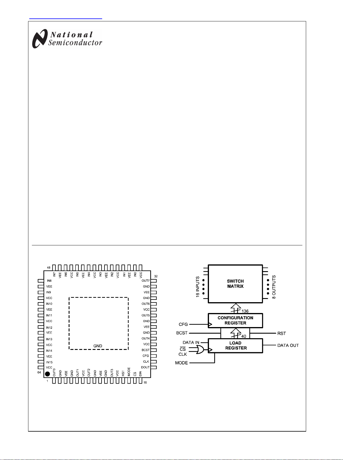
LMH6583 has 16 inputs and 8 outputs. The non-blocking architecture allows an output to be connected to any input,
including an input that is already selected. With fully buffered
inputs the LMH6583 can be impedance matched to nearly any
source impedance. The buffered outputs of the LMH6583 can
drive up to two back terminated video loads (75Ω load). The
outputs and inputs also feature high impedance inactive
states allowing high performance input and output expansion
for array sizes such as 16 x 16 or 32 x 8 by combining two
devices. The LMH6583 is controlled with a 4 pin serial interface. Both single serial mode and addressed chain modes are
available.
The LMH6583 comes in a 64-pin thermally enhanced TQFP
package. It also has diagonally symmetrical pin assignments
to facilitate double sided board layouts and easy pin connections for expansion.
Connection Diagram
Features
16 inputs and 8 outputs
■
64-pin exposed pad TQFP package
■
−3 dB bandwidth (V
■
−3 dB bandwidth (V
■
Fast slew rate 2200 V/μs
■
Channel to channel crosstalk (10/ 100 MHz) −70/ −52 dBc
■
All Hostile Crosstalk (10/ 100 MHz) −55/−45 dBc
■
Easy to use serial programming 4 wire bus
■
Two programming modes
■
Symmetrical pinout facilitates expansion.
■
Output current ±60 mA
■
Two gain options AV = 1 or AV = 2
■
= 2 VPP, RL = 1 kΩ) 550 MHz
OUT
= 2 VPP,RL = 150Ω) 450 MHz
OUT
Serial & addressed modes
Applications
Studio monitoring/production video systems
■
Conference room multimedia video systems
■
KVM (keyboard video mouse) systems
■
Security/surveillance systems
■
Multi antenna diversity radio
■
Video test equipment
■
Medical imaging
■
Wide-band routers & switches
■
Block Diagram
20150411
20150402
LMH® is a registered trademark of National Semiconductor Corporation.
TRI-STATE® is a registered trademark of National Semiconductor Corporation.
© 2007 National Semiconductor Corporation 201504 www.national.com

Absolute Maximum Ratings (Note 1)
If Military/Aerospace specified devices are required,
please contact the National Semiconductor Sales Office/
LMH6583
Distributors for availability and specifications.
ESD Tolerance (Note 2)
Human Body Model 2000V
Machine Model 200V
V
S
IIN (Input Pins)
I
OUT
Input Voltage Range V− to V
±6.2V
±20 mA
(Note 3)
Storage Temperature Range −65°C to +150°C
Soldering Information
Infrared or Convection (20 sec.) 235°C
Wave Soldering (10 sec.) 260°C
Operating Ratings (Note 1)
Temperature Range (Note 4) −40°C to +85°C
Supply Voltage Range ±3V to ±5.5V
Thermal Resistance
+
64–Pin Exposed Pad TQFP 27°C/W 0.82°C/W
θ
JA
Maximum Junction Temperature +150°C
±3.3V Electrical Characteristics (Note 5)
Unless otherwise specified, typical conditions are: TA = 25°C, AV = +2, VS = ±3.3V, RL = 100Ω; Boldface limits apply at the
temperature extremes.
θ
JC
Symbol Parameter Conditions Min
(Note 8)
Typ
(Note 7)
Max
(Note 8)
Units
Frequency Domain Performance
SSBW −3 dB Bandwidth V
LSBW
GF 0.1 dB Gain Flatness
DG Differential Gain
DP Differential Phase
= 0.5 V
OUT
V
OUT
V
OUT
V
OUT
PP
= 2 VPP, RL = 1 kΩ
= 2 VPP, RL = 150Ω
= 2 VPP, RL = 150Ω
RL = 150Ω, 3.58 MHz/ 4.43 MHz
RL = 150Ω, 3.58 MHz/ 4.43 MHz
425
500
MHz
450
80
MHz
%
deg
Time Domain Response
t
r
t
f
Rise Time 2V Step, 10% to 90% 1.7 ns
Fall Time 2V Step, 10% to 90% 1.4 ns
OS Overshoot 2V Step 4 %
SR Slew Rate 6 VPP, 10% to 90% (Note 6) 2000 V/µs
t
s
Settling Time 2V Step, V
within 0.1% ns
OUT
Distortion And Noise Response
HD2 2nd Harmonic Distortion 2 VPP, 10 MHz −76 dBc
HD3 3rd Harmonic Distortion 2 VPP, 10 MHz −76 dBc
e
n
i
n
Input Referred Voltage Noise >1 MHz 12
Input Referred Noise Current >1 MHz 2
nV/
pA/
Switching Time ns
XTLK Crosstalk All Hostile, f = 100 MHz −45 dBc
ISOL Off Isolation f = 100 MHz −60 dBc
Static, DC Performance
A
V
V
OS
TCV
I
B
TCI
V
O
V
O
B
Gain 1.986 2.00 2.014
Output Offset Voltage ±3 ±17 mV
Output Offset Voltage Average Drift (Note 10) 19 µV/°C
OS
Input Bias Current
Input Bias Current Average Drift
Output Voltage Range
Output Voltage Range
Non-Inverting (Note 9) −5
Non-Inverting (Note 10)
RL = 100Ω
RL = ∞ (Note 11)
±1.75 ±2.1 V
+2.1
±2.2 V
µA
nA/°C
-2.05
PSRR Power Supply Rejection Ratio 45 dB
I
CC
Positive Supply Current
RL = ∞
70 98 120 mA
www.national.com 2
LMH6583
Symbol Parameter Conditions Min
(Note 8)
I
EE
Negative Supply Current
RL = ∞
65 92 115 mA
Typ
(Note 7)
Max
(Note 8)
Units
Tri State Supply Current RST Pin > 2.0V 8 17 25 mA
Miscellaneous Performance
R
IN
C
IN
R
O
R
O
CMVR Input Common Mode Voltage
Input Resistance Non-Inverting 100
kΩ
Input Capacitance Non-Inverting 1 pF
Output Resistance Enabled Closed Loop, Enabled 300
Output Resistance Disabled Disabled 1100 1350 1450
mΩ
Ω
±1.3 V
Range
I
O
Output Current Sourcing, VO = 0 V ±50 mA
Digital Control
V
IH
V
IL
V
OH
V
OL
T
S
T
H
Input Voltage High 2.0 3.3 V
Input Voltage Low 0 0.8 V
Output Voltage High 2.2 V
Output Voltage Low 0.4 V
Setup Time 7 ns
Hold Time 7 ns
±5V Electrical Characteristics (Note 5)
Unless otherwise specified, typical conditions are: TA = 25°C, AV = +2, VS = ±5V, RL = 100Ω; Boldface limits apply at the tem-
perature extremes.
Symbol Parameter Conditions Min
(Note 8)
Typ
(Note 7)
Max
(Note 8)
Units
Frequency Domain Performance
SSBW −3 dB Bandwidth V
LSBW
GF 0.1 dB Gain Flatness
DG Differential Gain
DP Differential Phase
= 0.5 VPP (Note 11) 475
OUT
V
= 2 VPP, RL = 1 kΩ
OUT
V
= 2 VPP, RL = 150Ω
OUT
V
= 2 VPP, RL = 150Ω
OUT
RL = 150Ω, 3.58 MHz/ 4.43 MHz
RL = 150Ω, 3.58 MHz/ 4.43 MHz
550
450
100 MHz
%
deg
MHz
Time Domain Response
t
r
t
f
Rise Time 2V Step, 10% to 90% 1.4 ns
Fall Time 2V Step, 10% to 90% 1.3
ns
OS Overshoot 2V Step 2 %
SR Slew Rate 6 VPP, 10% to 90% (Note 6) 2200 V/µs
t
s
Settling Time 2V Step, V
Within 0.1% ns
OUT
Distortion And Noise Response
HD2 2nd Harmonic Distortion 2 VPP, 5 MHz −80 dBc
HD3 3rd Harmonic Distortion 2 VPP, 5 MHz −70 dBc
e
n
i
n
Input Referred Voltage Noise >1 MHz 12
Input Referred Noise Current >1 MHz 2
nV/
pA/
Switching Time ns
XTLK Cross Talk All Hostile, f = 100 MHz −45 dBc
Channel to Channel, f = 100 MHz −52 dBc
ISOL Off Isolation f = 100 MHz −65 dBc
Static, DC Performance
A
V
Gain LMH6583 1.986 2.00 2.014
3 www.national.com

Symbol Parameter Conditions Min
V
OS
LMH6583
TCV
I
B
TCI
B
V
O
Offset Voltage Input Referred ±2 ±17 mV
Output Offset Voltage Average Drift (Note 10) 38 µV/°C
OS
Input Bias Current
Input Bias Current Average Drift
Output Voltage Range
Non-Inverting (Note 9) −1 −5 −12 µA
Non-Inverting (Note 10) −12 nA/°C
RL = 100Ω
(Note 8)
+3.3
Typ
(Note 7)
Max
(Note 8)
±3.6 V
−3.4
V
O
Output Voltage Range
RL = ∞
±3.7 ±3.9 V
PSRR Power Supply Rejection Ratio DC 42 45 dB
XTLK DC Crosstalk Rejection DC, Channel to Channel 58 90 dB
OISO DC Off Isloation DC 66 90 dB
I
CC
I
EE
Positive Supply Current
Negative Supply Current
RL = ∞
RL = ∞
85 110 130 mA
80 104 124 mA
Tri State Supply Current RST Pin > 2.0V 12 22 30 mA
Miscellaneous Performance
R
IN
C
IN
R
O
R
O
CMVR Input Common Mode Voltage
Input Resistance Non-Inverting 100
Input Capacitance Non-Inverting 1 pF
Output Resistance Enabled Closed Loop, Enabled 300
Output Resistance Disabled Disabled, Resistance to Ground 1100 1300 1450
±3.0 V
Range
I
O
Output Current Sourcing, VO = 0 V ±60 mA
Digital Control
V
IH
V
IL
V
OH
V
OL
T
S
T
H
Input Voltage High 2.0 5.0 V
Input Voltage Low 0 0.8 V
Output Voltage High 2.4 V
Output Voltage Low 0.4 V
Setup Time 5 ns
Hold Time 5 ns
Units
kΩ
mΩ
Ω
Note 1: Absolute Maximum Ratings indicate limits beyond which damage to the device may occur. Operating Ratings indicate conditions for which the device is
intended to be functional, but specific performance is not guaranteed. For guaranteed specifications, see the Electrical Characteristics tables.
Note 2: Human Body Model, applicable std. MIL-STD-883, Method 3015.7. Machine Model, applicable std. JESD22-A115-A (ESD MM std. of JEDEC)
Field-Induced Charge-Device Model, applicable std. JESD22-C101-C (ESD FICDM std. of JEDEC).
Note 3: The maximum output current (I
Note 4: The maximum power dissipation is a function of T
PD = (T
Note 5: Electrical Table values apply only for factory testing conditions at the temperature indicated. No guarantee of parametric performance is indicated in the
electrical tables under conditions different than those tested.
Note 6: Slew Rate is the average of the rising and falling edges.
Note 7: Typical values represent the most likely parametric norm as determined at the time of characterization. Actual typical values may vary over time and will
also depend on the application and configuration. The typical values are not tested and are not guaranteed on shipped production material.
Note 8: Room Temperature limits are 100% production tested at 25°C. Factory testing conditions result in very limited self-heating of the device such that TJ =
TA. Limits over the operating temperature range are guaranteed through correlation using Statistical Quality Control (SQC) methods.
Note 9: Negative input current implies current flowing out of the device.
Note 10: Drift determined by dividing the change in parameter at temperature extremes by the total temperature change.
Note 11: This parameter is guaranteed by design and/or characterization and is not tested in production.
– TA)/ θJA. All numbers apply for packages soldered directly onto a PC Board.
J(MAX)
) is determined by device power dissipation limitations.
OUT
, θJA. The maximum allowable power dissipation at any ambient temperature is
J(MAX)
Ordering Information
Package Part Number Package Marking Transport Media NSC Drawing
64-Pin QFP LMH6583YA LMH6583YA 160 Units/Tray VXE64A
www.national.com 4
Typical Performance Characteristics
LMH6583
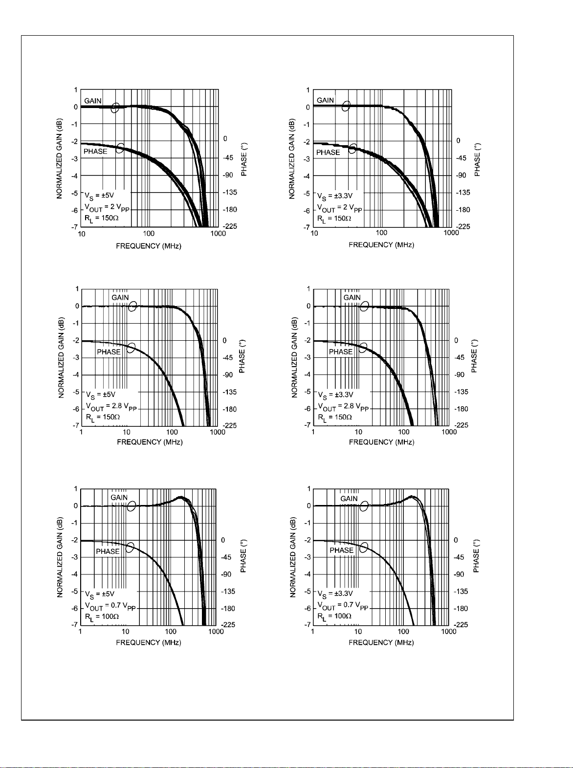
2 VPP Frequency Response
Large Signal Bandwidth
20150448
2 VPP Frequency Response
20150449
Large Signal Bandwidth
Small Signal Bandwidth
20150422
20150424
20150423
Small Signal Bandwidth
20150425
5 www.national.com

LMH6583
Frequency Response 1 kΩ Load
Group Delay
2 VPP Pulse Response
4 VPP Pulse Response
20150445
20150414
20150441
2 VPP Pulse Response
20150413
4 VPP Pulse Response Broadcast
20150416
www.national.com 6
20150417

LMH6583
4 VPP Pulse Response
2 VPP Off Isolation
20150415
6 VPP Pulse Response
20150418
2 VPP Crosstalk
2 VPP All Hostile Crosstalk
20150419
20150421
20150420
Second Order Distortion (HD2) vs. Frequency
20150427
7 www.national.com

LMH6583
Third Order Distortion (HD3) vs. Frequency
Second Order Distortion vs. Frequency
Third Order Distortion vs. Frequency
Positive Swing over Temperature
20150426
20150429
20150428
No Load Output Swing
20150434
Negative Swing Over Temperature
20150438
www.national.com 8
20150439

LMH6583
No Load Output Swing
Negative Swing over Temperature
20150431
Positive Swing over Temperature
20150436
Enabled Output Impedance
Disabled Output Impedance
20150437
20150451
20150450
9 www.national.com

Application Information
INTRODUCTION
The LMH6583 is a high speed, fully buffered, non blocking,
LMH6583
analog crosspoint switch. Having fully buffered inputs allows
the LMH6583 to accept signals from low or high impedance
sources without the worry of loading the signal source. The
fully buffered outputs will drive 75Ω or 50Ω back terminated
transmission lines with no external components other than the
termination resistor. When disabled, the outputs are in a high
impedance state. The LMH6583 can have any input connected to any (or all) output(s). Conversely, a given output can
have only one associated input.
INPUT AND OUTPUT EXPANSION
The LMH6583 has high impedance inactive states for both
inputs and outputs allowing maximum flexibility for Crosspoint
expansion. In addition the LMH6583 employs diagonal symmetry in pin assignments. The diagonal symmetry makes it
easy to use direct pin to pin vias when the parts are mounted
on opposite sides of a board. As an example two LMH6583
chips can be combined on one board to form either an 16 x
16 crosspoint or a 32 x 8 crosspoint. To make a 16 x 16 crosspoint all 16 input pins would be tied together (Input 0 on side
1 to input 15 on side 2 and so on) while the 8 output pins on
each chip would be left separate. To make the 32 x 8 crosspoint, the 8 outputs would be tied together while all 32 inputs
would remain independent. In the 32 x 8 configuration it is
important not to have 2 connected outputs active at the same
time. With the 16 x 16 configuration, on the other hand, having
two connected inputs active is a valid state. Crosspoint expansion as detailed above has the advantage that the signal
path has only one crosspoint in it at a time. Expansion methods that have cascaded stages will suffer bandwidth loss far
greater than the small loading effect of parallel expansion.
Output expansion is very straight forward. Connecting the inputs of two crosspoint switches has a very minor impact on
performance. Input expansion requires more planning. As
show in Figure 1 and Figure 2 there are two ways to connect
the outputs of the crosspoint switches. In Figure 2 the crosspoint switch outputs are connected directly together and
share one termination resistor. This is the easiest configuration to implement and has only one drawback. Because the
disabled output of the unused crosspoint (only one output can
be active at a time) has a small amount of capacitance the
frequency response of the active crosspoint will show peaking. This is illustrated in Figure 4 and Figure 5. In most cases
this small amount of peaking is not a problem.
As illustrated in Figure 1 each crosspoint output can be given
its own termination resistor. This results in a frequency response nearly identical to the non expansion case. There is
one drawback for the gain of 2 crosspoint, and that is gain
error. With a 75Ω termination resistor the 1250Ω resistance
of the disabled crosspoint output will cause a gain error. In
order to counter act this the termination resistors of both
crosspoints should be adjusted to approximately 80Ω. This
will provide very good matching, but the gain accuracy of the
system will now be dependent on the process variations of
the crosspoint resistors which have a variability of approximately ±20%.
20150442
FIGURE 1. Output Expansion
20150443
FIGURE 2. Input Expansion with Shared Termination
Resistors
www.national.com 10

20150444
FIGURE 3. Input Expansion with Separate Termination
Resistors
20150447
FIGURE 5. Input Expansion Frequency Response
DRIVING CAPACITIVE LOADS
Capacitive output loading applications will benefit from the
use of a series output resistor R
5 pF to 120 pF are the most critical, causing ringing, frequency
. Capacitive loads of
OUT
response peaking and possible oscillation. The chart “Suggested R
selecting a series output resistor for mitigating capacitive
vs. Cap Load” gives a recommended value for
OUT
loads. The values suggested in the charts are selected for 0.5
dB or less of peaking in the frequency response. This gives a
good compromise between settling time and bandwidth. For
applications where maximum frequency response is needed
and some peaking is tolerable, the value of R
duced slightly from the recommended values. When driving
can be re-
OUT
transmission lines the 50Ω or 75Ω matching resistor makes
the series output resistor unnecessary.
LMH6583
20150446
FIGURE 4. Input Expansion Frequency Response
USING OUTPUT BUFFERING TO ENHANCE BANDWIDTH
AND INCREASE RELIABILITY
The LMH6583 crosspoint switch can offer enhanced bandwidth and reliability with the use of external buffers on the
outputs. The bandwidth is increased by unloading the outputs
and driving the high impedance of an external buffer. See the
Frequency Response 1 kΩ Load curve in the Typical Performance section for an example of bandwidth achieved with
less loading on the outputs. For this technique to provide
maximum benefit a very high speed amplifier such as the
LMH6703 should be used. As shown in Figure 6 the resistor
R
is placed between the crosspoint output and the buffer
OUT
amplifier. This resistor will isolate the amplifier input capacitance and board capacitance from the crosspoint switch output. This resistor may not be needed if the amplifier is very
close to the crosspoint output. Any traces longer than 1 cm
will most likely require some termination resistance.
Besides offering enhanced bandwidth performance using an
external buffer provides for greater system reliability. The first
advantage is to reduce thermal loading on the crosspoint
switch. This reduced die temperature will increase the life of
the crosspoint. The second advantage is enhanced ESD reliability. It is very difficult to build high speed devices that can
withstand all possible ESD events. With external buffers the
crosspoint switch is isolated from ESD events on the external
system connectors.
11 www.national.com

LMH6583
FIGURE 6. Buffered Output
In this example R
the LMH6703 input capacitance from the crosspoint output.
The resistor RL is optional. It may improve performance by
providing a small DC load for the LMH6583 output stage
CROSSTALK
When designing a large system such as a video router
crosstalk can be a very serious problem. Extensive testing in
our lab has shown that most crosstalk is related to board layout rather than occurring in the crosspoint switch. There are
many ways to reduce board related crosstalk. Using controlled impedance lines is an important step. Using well decoupled power and ground planes will help as well. When
crosstalk does occur within the crosspoint switch itself it is
often due to signals coupling into the power supply pins. Using
appropriate supply bypassing will help to reduce this mode of
coupling. Another suggestion is to place as much grounded
copper as possible between input and output signal traces.
Care must be taken, though, not to influence the signal trace
impedances by placing shielding copper too closely. One other caveat to consider is that as shielding materials come
closer to the signal trace the trace needs to be smaller to keep
the impedance from falling too low. Using thin signal traces
will result in unacceptable losses due to trace resistance. This
effect becomes even more pronounced at higher frequencies
due to the skin effect. The skin effect reduces the effective
thickness of the trace as frequency increases. Resistive losses make crosstalk worse because as the desired signal is
attenuated with higher frequencies crosstalk increases at
higher frequencies.
DIGITAL CONTROL
may improve settling time by isolating
OUT
Block Diagram
FIGURE 7.
20150440
20150411
The LMH6583 has internal control registers that store the
programming states of the crosspoint switch. The logic is two
staged to allow for maximum programming flexibility. The first
stage of the control logic is tied directly to the crosspoint
switching matrix. This logic consists of one register for each
output that stores the on/off state and the address of which
input to connect to. These registers are not directly accessible
by the user. The second level of logic is another bank of registers identical to the first, but set up as shift registers. These
registers are accessed by the user via the serial input bus. As
described further below, there are two modes for programing
the LMH6582, Serial Mode and Addressed Mode.
The LMH6583 is programmed via a serial input bus with the
support of 4 other digital control pins. The Serial bus consists
of a clock pin (CLK), a serial data in pin (DIN), and a serial
data out pin (D
pin (CS). The chip select pin is active low. While the chip se-
). The serial bus is gated by a chip select
OUT
lect pin is high all data on the serial input pin and clock pins
is ignored. When the chip select pin is brought low the internal
logic is set to begin receiving data by the first positive transition (0 to 1) of the clock signal. The chip select pin must be
brought low at least 5 ns before the first rising edge of the
clock signal. The first data bit is clocked in on the next negative transition (1 to 0) of the clock signal. All input data is read
from the bus on the negative edge of the clock signal. Once
the last valid data has been clocked in, the chip select pin
must go high then the clock signal must make at least one
more low to high transition. Otherwise invalid data will be
clocked into the chip. The data clocked into the chip is not
transferred to the crosspoint matrix until the CFG pin is pulsed
high. This is the case regardless of the state of the Mode pin.
The CFG pin is not dependent on the state of the Chip select
pin. If no new data is clocked into the chip subsequent pulses
on the CFG pin will have no effect on device operation.
There are two ways to connect the serial data pins. The first
way is to control all 4 pins separately, and the second option
is to connect the CFG and the CS pins together for a 3 wire
interface. The benefit of the 4 wire interface is that the chip
can be configured independently of the CS pin. This would be
an advantage in a system with multiple crosspoint chips
where all of them could be programmed ahead of time and
then configured simultaneously. The 4 wire solution is also
helpful in a system that has a free running clock on the CLK
pin. In this case, the CS pin needs to be brought high after the
last valid data bit to prevent invalid data from being clocked
into the chip.
The three wire option provides the advantage of one less pin
to control at the expense of having less flexibility with the
configure pin. One way around this loss of flexibility would be
If the clock signal is generated by an FPGA or microcontroller
where the clock signal can be stopped after the data is
clocked in. In this case the Chip select function is provided by
the presence or absence of the clock signal.
The programming format of the incoming serial data is selected by the MODE pin. When the mode pin is HIGH the
crosspoint can be programmed one output at a time by entering a string of data that contains the address of the output
that is going to be changed (Addressed Mode). When the
mode pin is LOW the crosspoint is in Serial Mode. In this
mode the crosspoint accepts a 40 bit array of data that programs all of the outputs. In both modes the data fed into the
chip does not change the chip operation until the Configure
pin is pulsed high. The configure and mode pins are independent of the chip select pin.
www.national.com 12

LMH6583
SERIAL PROGRAMMING MODE
Serial programming mode is the mode selected by bringing
the MODE pin low. In this mode a stream of 40 bits programs
all 8 outputs of the crosspoint. The data is fed to the chip as
shown in the Serial Mode Data Frame tables below (4 tables
are required to show the entire data frame). The table is arranged such that the first bit clocked into the crosspoint
register is labeled bit number 0. The register labeled Load
Register in the block diagram is a shift register. If the chip
select pin is left low after the valid data is shifted into the chip
and if the clock signal keeps running then additional data will
be shifted into the register, and the desired data will be shifted
out.
Also illustrated is the timing relationships for the digital pins
in the Timing Diagram for Serial Mode shown below. It is im-
portant to note that all the pin timing relationships are important, not just the data and clock pins. One example is that the
Chip Select pin (CS) must transition low before the first rising
edge of the clock signal. This allows the internal timing circuits
to synchronize to allow data to be accepted on the next falling
edge. After the final data bit has been clocked in, the chip
select pin must go high, then the clock signal must make at
least one more low to high transition. As shown in the timing
diagram, the chip select pin state should always occur while
the clock signal is low. The configure (CFG) pin timing is not
so critical, but it does need to be kept low until all data has
been shifted into the crosspoint registers.
Timing Diagram for Serial Mode
Serial Mode Data Frame (First 2 Words)
Output 0 Output 1
Input Address On = 0 Input Address On = 0
LSB MSB Off = 1 LSB MSB Off = 1
0 1 2 3 4 5 6 7 8 9
Off = TRI-STATE®, Bit 0 is first bit clocked into device.
Serial Mode Data Frame (Continued)
Output 2 Output 3
Input Address On = 0 Input Address On = 0
LSB MSB Off = 1 LSB MSB Off = 1
10 11 12 13 14 15 16 17 18 19
20150409
13 www.national.com

Serial Mode Data Frame (Continued)
LMH6583
Output 4 Output 5
Input Address On = 0 Input Address On = 0
LSB MSB Off = 1 LSB MSB Off = 1
20 21 22 23 24 25 26 27 28 29
Serial Mode Data Frame (Last 2 Words)
Output 6 Output 7
Input Address On = 0 Input Address On = 0
LSB MSB Off = 1 LSB MSB Off = 1
30 31 32 33 34 35 36 37 38 39
Bit 39 is last bit clocked into device.
ADDRESSED PROGRAMMING MODE
Addressed programming mode makes it possible to change
only one output register at a time. To utilize this mode the
mode pin must be High. All other pins function the same as
in serial programming mode except that the word clocked in
is 8 bits and is directed only at the output specified. In addressed mode the data format is shown below in the table
titled Addressed Mode Word Format.
Also illustrated is the timing relationships for the digital pins
in the Timing Diagram for Addressed Mode shown below. It
is important to note that all the pin timing relationships are
important, not just the data and clock pins. One example is
that the Chip Select pin (CS) must transition low before the
first rising edge of the clock signal. This allows the internal
timing circuits to synchronize to allow data to be accepted on
the next falling edge. After the final data bit has been clocked
in, the chip select pin must go high, then the clock signal must
make at least one more low to high transition. As shown in the
timing diagram, the chip select pin state should always occur
while the clock signal is low. The configure (CFG) pin timing
is not so critical, but it does need to be kept low until all data
has been shifted into the crosspoint registers.
Timing Diagram for Addressed Mode
www.national.com 14
20150410

Addressed Mode Word Format
Output Address Input Address TRI-STATE
LSB MSB LSB MSB 1 = TRI-STATE
0 1 2 3 4 5 6 7
Bit 0 is first bit clocked into device.
DAISY CHAIN OPTION IN SERIAL MODE
The LMH6583 supports daisy chaining of the serial data
stream between multiple chips. This feature is available only
in the Serial programming mode. To use this feature serial
data is clocked into the first chip DIN pin, and the next chip
DIN pin is connected to the DOUT pin of the first chip. Both
chips may share a chip select signal, or the second chip can
be enabled separately. When the chip select pin goes low on
both chips a double length word is clocked into the first chip.
As the first word is clocking into the first chip the second chip
is receiving the data that was originally in the shift register of
the first chip (invalid data). When a full 40 bits have been
clocked into the first chip the next clock cycle begins moving
the first frame of the new configuration data into the second
chip. With a full 80 clock cycles both chips have valid data and
the chip select pin of both chips should be brought high to
prevent the data from overshooting. A configure pulse will activate the new configuration on both chips simultaneously, or
each chip can be configured separately. The mode, chip select, configure and clock pins of both chips can be tied together and driven from the same sources.
SPECIAL CONTROL PINS
The LMH6583 has two special control pins that function independent of the serial control bus. One of these pins is the
reset (RST) pin. The RST pin is active high meaning that a
logic 1 level the chip is configured with all outputs disabled
and in a high impedance state. The RST pin programs all the
registers with input address 0 and all the outputs are turned
off. In this configuration the device draws only 20 mA. The
reset pin can used as a shutdown function to reduce power
consumption. The other special control pin is the broadcast
(BCST) pin. The BCST pin is also active high and sets all the
outputs to the on state connected to input 0. This is sometimes
referred to as broadcast mode, where input 0 is broadcast to
all 8 outputs.
THERMAL MANAGEMENT
The LMH6583 is packaged in a thermally enhanced Quad Flat
Pack package. Even so, it is a high performance device that
produces a significant amount of heat. With a ±5V supply, the
LMH6583 will dissipate approximately 1.1W of idling power
LMH6583
0 = On
with all outputs enabled. Idling power is calculated based on
the typical supply current of 110 mA and a 10V supply voltage.
This power dissipation will vary within the range of 800 mW
to 1.4W due to process variations. In addition, each equivalent video load (150Ω) connected to the outputs should be
budgeted 30 mW of power. For a typical application with one
video load for each output this would be a total power of 1.14
W. With a θJA of 27°C/W this will result in the silicon being 31°
C over the ambient temperature. A more aggressive application would be two video loads per output which would result
in 1.38 W of power dissipation. This would result in a 37°C
temperature rise. For heavier loading, the QFP package thermal performance can be significantly enhanced with an external heat sink and by providing for moving air ventilation.
Also, be sure to calculate the increase in ambient temperature
from all devices operating in the system case. Because of the
high power output of this device, thermal management should
be considered very early in the design process. Generous
passive venting and vertical board orientation may avoid the
need for fan cooling or heat sinks. Also, the LMH6583 can be
operated with a ±3.3V power supply. This will cut power dissipation substantially while only reducing bandwidth by about
10% (2 VPP output). The LMH6583 is fully characterized and
factory tested at the ±3.3V power supply condition for applications where reduced power is desired.
PRINTED CIRCUIT LAYOUT
Generally, a good high frequency layout will keep power supply and ground traces away from the input and output pins.
Parasitic capacitances on these nodes to ground will cause
frequency response peaking and possible circuit oscillations
(see Application Note OA-15 for more information). If digital
control lines must cross analog signal lines (particularly inputs) it is best if they cross perpendicularly. National Semiconductor suggests the following evaluation boards as a
guide for high frequency layout and as an aid in device testing
and characterization:
Device Package Evaluation Board
Part Number
LMH6583 64-Pin TQFP LMH730156
15 www.national.com

Physical Dimensions inches (millimeters) unless otherwise noted
LMH6583
64-Pin Exposed Pad QFP
NS Package Number VXE64A
www.national.com 16

Notes
LMH6583
17 www.national.com

Notes
THE CONTENTS OF THIS DOCUMENT ARE PROVIDED IN CONNECTION WITH NATIONAL SEMICONDUCTOR CORPORATION
(“NATIONAL”) PRODUCTS. NATIONAL MAKES NO REPRESENTATIONS OR WARRANTIES WITH RESPECT TO THE ACCURACY
OR COMPLETENESS OF THE CONTENTS OF THIS PUBLICATION AND RESERVES THE RIGHT TO MAKE CHANGES TO
SPECIFICATIONS AND PRODUCT DESCRIPTIONS AT ANY TIME WITHOUT NOTICE. NO LICENSE, WHETHER EXPRESS,
IMPLIED, ARISING BY ESTOPPEL OR OTHERWISE, TO ANY INTELLECTUAL PROPERTY RIGHTS IS GRANTED BY THIS
DOCUMENT.
TESTING AND OTHER QUALITY CONTROLS ARE USED TO THE EXTENT NATIONAL DEEMS NECESSARY TO SUPPORT
NATIONAL’S PRODUCT WARRANTY. EXCEPT WHERE MANDATED BY GOVERNMENT REQUIREMENTS, TESTING OF ALL
PARAMETERS OF EACH PRODUCT IS NOT NECESSARILY PERFORMED. NATIONAL ASSUMES NO LIABILITY FOR
APPLICATIONS ASSISTANCE OR BUYER PRODUCT DESIGN. BUYERS ARE RESPONSIBLE FOR THEIR PRODUCTS AND
APPLICATIONS USING NATIONAL COMPONENTS. PRIOR TO USING OR DISTRIBUTING ANY PRODUCTS THAT INCLUDE
NATIONAL COMPONENTS, BUYERS SHOULD PROVIDE ADEQUATE DESIGN, TESTING AND OPERATING SAFEGUARDS.
LMH6583 16x8 550 MHz Analog Crosspoint Switch, Gain of 2
EXCEPT AS PROVIDED IN NATIONAL’S TERMS AND CONDITIONS OF SALE FOR SUCH PRODUCTS, NATIONAL ASSUMES NO
LIABILITY WHATSOEVER, AND NATIONAL DISCLAIMS ANY EXPRESS OR IMPLIED WARRANTY RELATING TO THE SALE
AND/OR USE OF NATIONAL PRODUCTS INCLUDING LIABILITY OR WARRANTIES RELATING TO FITNESS FOR A PARTICULAR
PURPOSE, MERCHANTABILITY, OR INFRINGEMENT OF ANY PATENT, COPYRIGHT OR OTHER INTELLECTUAL PROPERTY
RIGHT.
LIFE SUPPORT POLICY
NATIONAL’S PRODUCTS ARE NOT AUTHORIZED FOR USE AS CRITICAL COMPONENTS IN LIFE SUPPORT DEVICES OR
SYSTEMS WITHOUT THE EXPRESS PRIOR WRITTEN APPROVAL OF THE CHIEF EXECUTIVE OFFICER AND GENERAL
COUNSEL OF NATIONAL SEMICONDUCTOR CORPORATION. As used herein:
Life support devices or systems are devices which (a) are intended for surgical implant into the body, or (b) support or sustain life and
whose failure to perform when properly used in accordance with instructions for use provided in the labeling can be reasonably expected
to result in a significant injury to the user. A critical component is any component in a life support device or system whose failure to perform
can be reasonably expected to cause the failure of the life support device or system or to affect its safety or effectiveness.
National Semiconductor and the National Semiconductor logo are registered trademarks of National Semiconductor Corporation. All other
brand or product names may be trademarks or registered trademarks of their respective holders.
Copyright© 2007 National Semiconductor Corporation
For the most current product information visit us at www.national.com
www.national.com
National Semiconductor
Americas Customer
Support Center
Email:
new.feedback@nsc.com
Tel: 1-800-272-9959
National Semiconductor Europe
Customer Support Center
Fax: +49 (0) 180-530-85-86
Email: europe.support@nsc.com
Deutsch Tel: +49 (0) 69 9508 6208
English Tel: +49 (0) 870 24 0 2171
Français Tel: +33 (0) 1 41 91 8790
National Semiconductor Asia
Pacific Customer Support Center
Email: ap.support@nsc.com
National Semiconductor Japan
Customer Support Center
Fax: 81-3-5639-7507
Email: jpn.feedback@nsc.com
Tel: 81-3-5639-7560
 Loading...